

Page 1
CLC016
Data Retiming PLL with Automatic Rate Selection
General Description
National’s Comlinear CLC016 is a low-cost, monolithic, data
retiming phase-locked loop (PLL) designed for high-speed
serial clock and data recovery. The CLC016 simplifies highspeed data recovery in multi-rate systems by incorporating
auto-rate select (ARS) circuitry on chip. This function allows
the user to configure the CLC016torecognize up to four different data rates and automatically adjust to provide accurate, low-jitter clock and data recovery. A single resistor is
used to set each data rate anywhere between 40 Mbps and
400 Mbps. No potentiometers, crystals, or other external ICs
are required to set the rate.
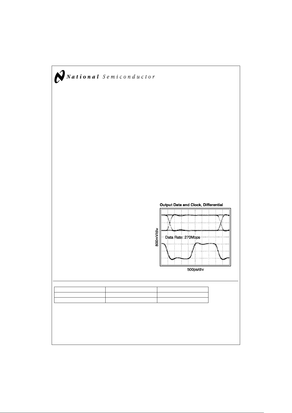
The CLC016 has output jitter of only 130 ps
pp
at a 270 Mbps
data rate and 0.25%fractional loop bandwidth. Low phase
detector output offset and low VCO injection combine to ensure that the CLC016 does not generate bit errors or large
phase transients in response to extreme fluctuations in data
transition density. The result is improved performance when
handling the pathological patterns inherent in the SMPTE
259M video industry standard.
The carrier detect and output mute functions may be used
together to automatically latch the outputs when no data is
present, preventing random transitions. The external loop filter allows the user to tailor the loop response to the specific
application needs. The CLC016 will operate with either +5V
or −5.2V power supplies. The serial data inputs and outputs,
as well as the recovered clock outputs, allow single- or
differential-ECL interfacing. The logic control inputs are TTLcompatible.
Applications
n SMPTE 259M serial digital interfaces: NTSC/PAL, 4:2:2
component, 360 Mbps wide screen
n Serial digital video routing and distribution
n Clock and data recovery for high-speed data
transmission
n Re-synchronization of serial data for SONET/SDH, ATM,
CAD networks, medical and industrial imaging
Features
n Retimed data output
n Recovered clock output
n Auto and manual rate select modes
n Four user-configurable data rates
n No potentiometers required
n External loop bandwidth control
n Frequency detector for lock acquisition
n Carrier detect output
n Output MUTE function
n Single supply operation: +5V or −5.2V
n Low cost
Key Specifications
n Low jitter: 130 ps
pp
@
270 Mbps, 0.25%fractional loop
bandwidth (0.675 MHz)
n High data rates: 40 Mbps − 400 Mbps
n Low supply current: 100 mA, including output biasing
n Flexible fractional loop bandwidth: from 0.05%to 0.5
%
Order Number Temperature Package
CLC016ACQ 0˚C to +70˚C PLCC V28A
CLC016AJQ –40˚C to +85˚C PLCC V28A
TRI-STATE®is a registered trademark of National Semiconductor Corporation.
DS100087-1
July 1998
CLC016 Data Retiming PLL with Automatic Rate Selection
© 1998 National Semiconductor Corporation DS100087 www.national.com
Page 2
Typical Application
Four-Rate Clock and Data Recovery with Automatic Rate Selection
DS100087-2
Pinout
DS100087-3
28-pin PLCC
www.national.com 2
Page 3
Absolute Maximum Ratings (Note 1)
If Military/Aerospace specified devices are required,
please contact the National Semiconductor Sales Office/
Distributors for availability and specifications.
Supply Voltage (V
CC–VEE
) −0.3, +6.0V
Maximum Junction Temperature +150˚C
Storage Temperature Range −65˚C to +150˚C
Lead Temperature (Soldering 4 sec) +260˚C
ESD Rating (Note 12) 2kV
Package Thermal Resistance
θ
JA
28-Pin PLCC 85˚C/W
θ
JC
28-Pin PLCC 35˚C/W
Reliability Information
MTTF (based on limited life
test data) 2.6 x 10
7
hours
Recommended Operating
Conditions
Supply Voltage (VCC–VEE) 4.5V to 5.5V
Operating Temperature –40˚C to +85˚C
Jitter Transfer Function Fractional Loop
Bandwidth 0.05%to 0.5
%
SCO/SCO, SDO/SDO Minimum
Voltage (Note 13) VCC– 1.6V
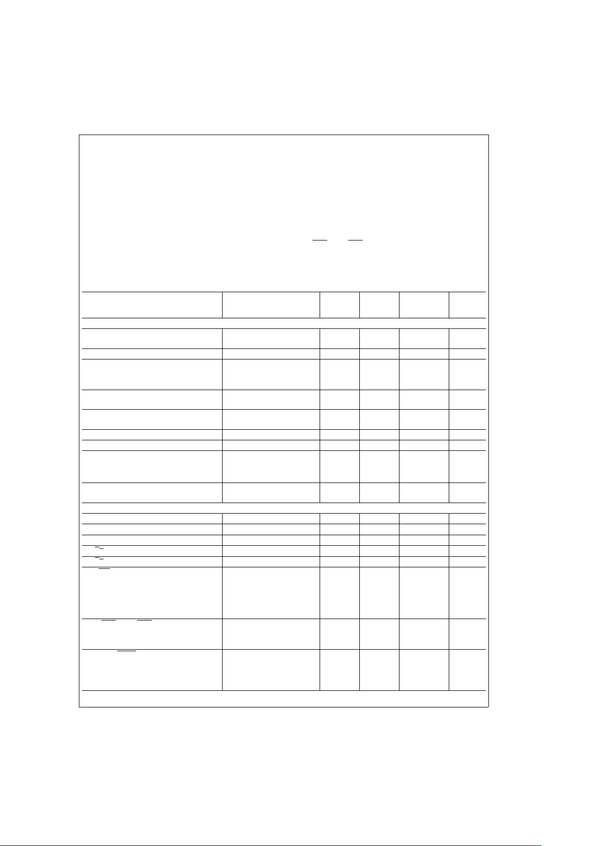
Electrical Characteristics
(VCC= 0V, VEE= −5V, RBW= 500Ω;CZ= 0.1 µF; CP= 82 pF; Rn= 3504, C
ARS
= 0.1 µF; unless specified).
Parameter Conditions
Typ
+25˚C
Min/Max
+25˚C
Min/Max
Full Temp.
Range
Units
DYNAMIC PERFORMANCE
Residual Jitter 270 Mbps PRN sequence
(Notes 3, 4)
150 250 300 ps
pp
Acquisition Time 270 Mbps PRN sequence 6 x 10
5
bit cells
Minimum Average Data Rate, f
CLK
Full Temperature Range
4.5V ≤ (V
CC−VEE
) ≤ 5.5V
(Note 3)
100 100 Mbps
0 to 70˚ 4.5V ≤ (V
CC−VEE
) ≤ 5.5V 40 Mbps
Maximum Average Data Rate, f
CLK
4.5V ≤ (VCC−VEE) ≤ 5.5V
(Note 3)
400 400 Mbps
Tracking and Capture Range 4.5V ≤ (V
CC−VEE
) ≤ 5.5V
(Notes 3, 5)
±
8.3
±
5.0/
±
13.0
±
2.5/
±
18.0
%
f
CLK
VCO Power Supply Sensitivity (Note 3)
±
0.8
±
1.2
±
1.3
%
V
VCO Temperature Sensitivity
±
250 ppm/˚C
Jitter Transfer Function −3 dB bandwidth
(Fractional Loop Bandwidth), λ
BW
RBW= 100Ω (Notes 6, 7) 0.05
%
f
CLK
RBW= 500Ω (Notes 6, 7) 0.25
%
f
CLK
RBW= 1000Ω (Notes 6, 7) 0.5
%
f
CLK
Jitter Transfer Function Peaking RBW= 500Ω, 270 Mbps
(Note 6)
<
0.1 dB
STATIC PERFORMANCE
Power Supply Current, I
EE
(Note 3) 105 125 133 mA
Voltage on Selected R
n
Resistor (Note 8) VCC−2.2 V
Voltage on Unselected R
n
Resistor (Note 8) V
CC
V
V
C/VC
Common-Mode Voltage, V
CM
(Note 8) VCC−1.5 V
V
C/VC
Diff-Mode Voltage Range, V
DM
(Note 8)
±
300 mV
DDI/DDI
Input Range Upper Limit, V
H
V
CC
V
Input Range Lower Limit, V
L
VEE+2.5 V
Minimum Differential Input Amplitude, V
∆
200 200 mV
Input Current (Note 3) 3 6 6 µA
SCO/SCO, SDO/SDO
Output Current, I
OUT
(Note 3) 11 9.3/12 8.6/12.7 mA
Output Voltage Swing, V
OUT
R
collector
=75Ω(Note 3) 725 625/900 mV
ACQ/WR, MUTE, RDO/RD1
Voltage Input — LOW, V
IL
(Note 9)
V
EE
+ 0.8 VEE+ 0.8 V
Voltage Input — HIGH, V
IH
(Note 3) VEE+ 2.0 VEE+ 2.0 V
Input Current (I
IN
) (Note 3)
±
100
±
500 nA
3 www.national.com
Page 4
Electrical Characteristics (Continued)
(VCC= 0V, VEE= −5V, RBW= 500Ω;CZ= 0.1 µF; CP= 82 pF; Rn= 3504, C
ARS
= 0.1 µF; unless specified).
Parameter Conditions
Typ
+25˚C
Min/Max
+25˚C
Min/Max
Full Temp.
Range
Units
STATIC PERFORMANCE
CD, UNL, RDO/RD1 (Note 9)
Current Output — LOW, I
OL
VOL≤ VEE+0.5V 800 µA
Current Output — HIGH, I
OH
VOH≥ VCC−0.5V −700 µA
TIMING PERFORMANCE
Delay: SCO to SDO, t
d
200 ps
SCO Duty Cycle (Note 3) 50 44/56 44/56
%
Rise/Fall Time: SCO, SDO, t
r/tf
20%–80%,R
collector
=75Ω
(Note 10)
230 ps
SDO Duty Cycle Distortion 35 ps
Minimum Setup Time:
RDO/RD1 to ACQ/WR, t
SU
420 20 ns
Minimum Hold Time:
ACQ/WR to SS1/SS0, t
h
320 20 ns
Minimum Pulse Width:
ACQ/WR, t
w
520 20 ns
ARS Oscillator Period, t
OSC
(Note 3) 10.5 8.5/15.5 ms
CD Pulse Width, t
PW
(Note 11) 1 µs
MUTE Response Time, t
M
5ns
Note 1: “Absolute Maximum Ratings” are those values beyond which the safety of the device cannot be guaranteed. They are not meant to imply that the devices
should be operated at these limits. The table of “Electrical Characteristics” specifies conditions of device operation.
Note 2: Min/Max ratings are based on product characterization and simulation. Individual parameters are tested as noted. Outgoing quality levels are determined
from tested parameters.
Note 3: J-level spec. is 100%tested at +25˚C.
Note 4: Peak-to-peak jitter is defined as 6 times the rms jitter.
Note 5: Tracking and capture range are specified as a percentage of the input data rate f
CLK
. The minimum and maximum are guaranteed so long as Rnhas been
chosen according to the equation in
Resistor Selection for Data Rates.
Note 6: Average data transition density of 1 transition per 2 bit cells.
Note 7: When the value of R
BW
changes it is necessary to also change the values of CPand CZ. See
Loop Filter Design.
Note 8: This information is provided for system troubleshooting purposes only.
Note 9: RD0/RD1 are inputs when AUTO = 0 and outputs when AUTO = 1.
Note 10: Includes typical pc board capacitance.
Note 11: The CD circuit is a retriggerable one-shot which retriggers on every data transition.
Note 12: Human body model, 1.5 kΩ in series with 100 pF.
Note 13: To maintain specified performance, SCO/SCO and SDO/SDO should not drop below this level.
www.national.com 4
Page 5
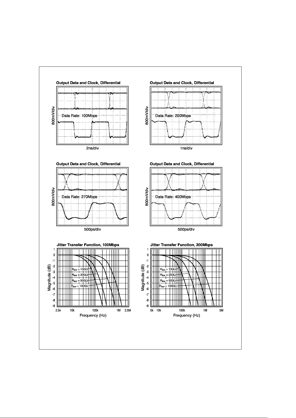
Typical Performance Characteristics
DS100087-4 DS100087-5
DS100087-6 DS100087-7
DS100087-8 DS100087-9
5 www.national.com
Page 6
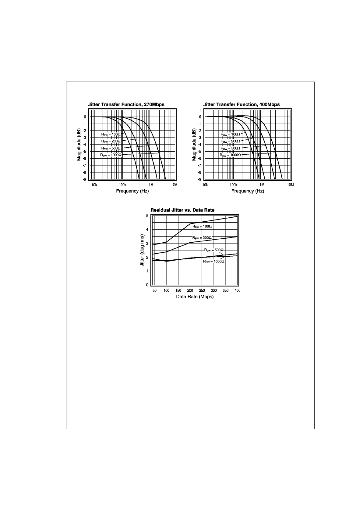
Typical Performance Characteristics (Continued)
DS100087-10 DS100087-11
DS100087-12
www.national.com 6
Page 7

Product Description
The CLC016 Data Retiming PLL is a monolithic circuit that
recovers clock and data from a serial NRZ or NRZI data
stream. The Data Retiming PLL incorporates an Auto-Rate
Selection function which automatically selects one of four
user-configurable data rates. The following outline lists the
material covered in this data sheet:
•
Typical schematics for +5V or −5.2V operation
•
Block diagram description
•
Pin definitions
•
Design guidelines
•
Interface connections
•
Measurement
•
Typical applications
•
Printed circuit layout and evaluation boards
For application assistance, refer to the list of telephone numbers on the pack page of this data sheet.
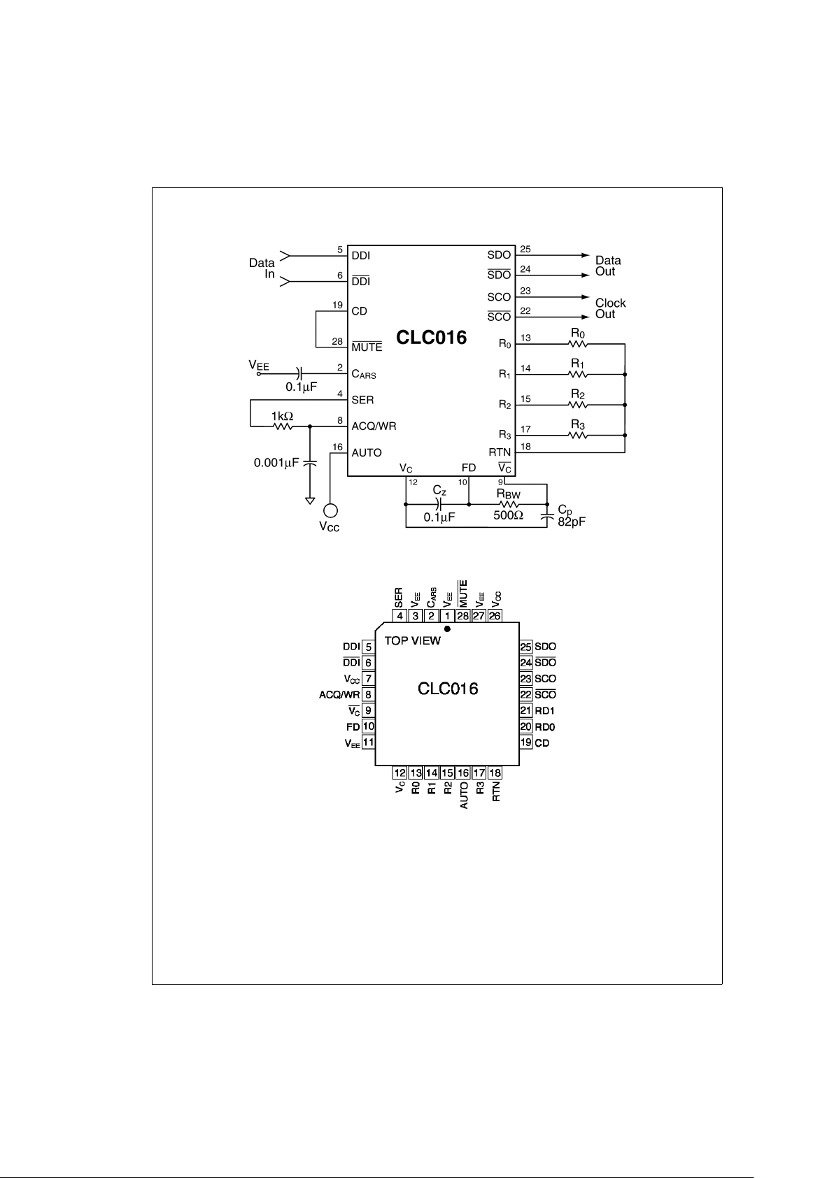
Data Retimer Typical Connections
The CLC016 schematics provided in
Figure 1
and
Figure 2
show typical +5V or −5.2V connections with Auto-Rate Selection configured for SMPTE 259M standard video data
rates: 143, 177, 270 and 360 Mbps. The section
Resistor
Selection for Data Rates
gives tables and equations for de-
termining R
n
resistor values for any data rate from 50 Mbps
to 400 Mbps. A resistor value table is also given for SONET/
SDH data rates. The schematics in
Figure 1
and
Figure 2
do
not include input termination. The high impedance inputs on
the CLC016 allow the user to define the termination. The
Interfaces
section suggests recommended terminations for
the inputs and outputs of the CLC016.
DS100087-13
FIGURE 1. Typical +5V Connection
DS100087-14
FIGURE 2. Typical −5.2V Connection
7 www.national.com
Page 8

Product Description (Continued)
Pin Definitions
Name Pin # Description
DDI, DDI
5, 6 Differential (ECL, PECL) data
inputs.
SCO,
SCO
23, 22 Differential collector (ECL,
PECL compatible) clock outputs
SDO,
SDO
25, 24 Differential collector (ECL,
PECL compatible) retimed data
outputs
RDO,
RD1
20, 21 Bi-directional (TTL, CMOS)
VCO data rate bus. See
Table 3
for state table.
R
n
13, 14,
15, 17
VCO rate configuration resistors
(n=0,1,2,3).
RTN 18 Return for R
n
SER 4 Loop unlock output (TTL,
CMOS) indicator. High when
loop is unlocked or
harmonic-locked.
CD 19 Carrier detector (TTL, CMOS)
output. Low when no signal is
present.
MUTE
28 Output mute (TTL, CMOS)
control. Connect to CD to latch
outputs when no signal is
present.
AUTO 16 Auto- or manual-rate mode
control (TTL, CMOS) input.
Assert high for auto-rate mode.
ACQ/WR 8 ARS oscillator enable and rate
latch enable (TTL, CMOS)
input. Connect to SER (see
diagrams) for auto-rate mode.
C
ARS
2 External capacitor connections
for controlling the rate of the
ARS search.
V
C,VC
12, 9 VCO control lines. Loop filter
connects across these and FD.
FD 10 Frequency detector output. C
Z
must connect from FD to VC.
V
CC
7, 26 Positive supply pins (ground or
+5V).
V
EE
1, 3, 11,27Negative supply pins (−5.2V or
ground).
Operation Description
The CLC016 Data Retiming PLL,
Figure 3
, has three main
functions: Frequency Detector (FD), Phase-Locked Loop
(PLL) and Auto-Rate Select (ARS).
The Frequency Detector detects the frequency difference
between the input data rate and the VCO frequency, and
forces a rapid change in VCO frequency to minimize that difference. As the frequency difference approaches zero, the
PLL acquires phase lock and the Frequency Detector becomes inactive. In Auto-Rate Select mode, the Frequency
Detector requests the ARS function to search for a new data
rate.
The PLL consists of a Voltage Controlled Oscillator (VCO), a
Phase Detector (PD), and an external Loop Filter (LF). The
PLL recovers a low-jitter clock for data retiming. The data is
re-synchronized (retimed) at the Data Latch. The data and
clock are buffered outputs.
TheARS block has two modes of operation:Auto-Rate Mode
(ARM) and Manual-Rate Mode (MRM). Once the ARS function is activated (ARM), it sequences through the userselected data rates until phase lock is achieved. The user
has control over the rate at which ARS steps through the
data rates (see
Auto-Rate Selection
section).
The Carrier Detect (CD) block detects the presence of input
data and is an input to the ARS block. When CD is connected to MUTE and no data is present, the clock and data
outputs are latched.
DS100087-15
FIGURE 3. Functional Block Diagram
www.national.com 8
Page 9
Product Description (Continued)
Functional Block Descriptions
Frequency Detector (FD)
The Frequency Detector detects the difference between
VCO rate and the input data rate, then forces the frequency
(rate) difference to zero. In Auto-Rate Mode, when a difference is detected, FD requests the ARS block to start a
search to match the rate. Once the PLL acquires phase lock,
the PLL takes control and the FD goes inactive.
Phase Detector (PD)
The PD compares the phase of the VCO to the phase of the
input data. The PD output is a differential current which is
proportional to the phase error. The PD gain has units of amperes per radian and is dependent upon the data transition
density (ρ). The data transition density is defined as the average number of data transitions per clock cycle, and is
bounded by 0 ≤ρ≤1. The PD output is connected to the
VCO through the external loop filter network. This network
translates the PD output current to a voltage that controls the
VCO.
Loop Filter (LF)
The external Loop Filter shown in
Figure 3
is made up of
passive components R
BW,CZ
, and CP. This external loop fil-
ter controls the PLL dynamics and acquisition time.
The Frequency Detector supplies its signal to the C
Z
capacitor, and takes control of the VCO under the condition of frequency unlock. The selection of the filter components is covered in the
Loop Filter Design
section.
Voltage Controlled Oscillator (VCO)
The VCO is a temperature-compensated, factory-trimmed
multivibrator that requires no external capacitors for tuning. It
is stable over temperature and power supply variations. This
eliminates the need for potentiometers to adjust each of the
VCO center frequencies to correspond with the input data
rates. Instead, an external resistor (R
n
) is used to set each of
four data rates in the range of 40 Mbps to 400 Mbps.
Carrier Detector (CD)
The CD circuit is a retriggerable one-shot which retriggers on
every data transition. When data transitions occur at a rate
≥1 transition per µs, CD indicates the presence of data at the
input pins DDI and DDI. CD also inputs a signal to ARS that
inhibits any rate search from occurring in the absence of input data. When CD in connected to the MUTE pin, and no
data is present, the output clock (SCO, SCO) and data
(SDO, SDO) lines are latched.
Auto-Rate Select (ARS) and Multiplexer (MUX)
The ARS, in conjunction with the MUX, sequences through
the user-configured resistor values (R
n
) in an unlocked condition. The ARS has two modes: Auto-Rate Mode (ARM) and
Manual-Rate Mode (MRM). It incorporates additional features and functions that are discussed in the section named
Auto-Rate Selection.
When ARS is in Auto-Rate Mode, its inputs are the FD (the
LHP control line), the Carrier Detect (CD), the VCO (CLK),
and Latched Data output. These input signals produce an
external Search (SER) signal that, when connected to the
ACQ/WR input, enables the ARM operation. A single capacitor, C
ARS
, sets the ARM sequence time for stepping through
the different user-configured data rates.
The timing section of the ARS block controls the digital input
analog multiplexer (MUX). Under the control of ARS, the
MUX steps through each data rate starting with the
previously-selected resistor R
n
and incrementing to R
n+1
,
etc. in order of R
0,R1,R2,R3,R0
, .... This sequence is re-
peated until lock is achieved. The 2-bit bidirectional bus,
comprised of RD0 and RD1, indicates the selected data rate.
The RD0, RD1 bidirectional bus is set to output mode when
AUTO is active (high). Therefore, RD0, RD1 can be monitored when AUTO is active. When no data is present at the
inputs, CD will inhibit the ARM.
In manual mode the RD0, RD1 lines are set to input mode.
Therefore, RD0, RD1 cannot be monitored when AUTO is inactive. The selection of external components for both modes
of operation is discussed in sections,
Resistor Selection for
Data Rates,
and
Auto-Rate Selection
.
DESIGN GUIDELINES
Resistor Selection for Data Rates
The CLC016 Data Retiming PPL supports 4 different data
rates using user-selected resistors that set the VCO center
frequency. The resistors found in
Figures 1, 2
are identified
by the reference designators R
n
, where n is 0, 1, 2 and 3.
It is recommended that the user select resistor values with
tolerances of 1%and temperature coefficients of ≤100 ppm/
˚C. Refer to
Table 1
and
Table 2
for calculated resistor values for SMPTE and SONET standards. Resistors for other
data rates are determined from the following equation:
wheren=0,1,2,3andf
CLK
is the desired data rate.
TABLE 1. Resistor Values for SMPTE 259M Data Rates
Data Rate
(Mbps)
Ref. Des.
(in
Figures
1, 2
)
R
n
Calculated
Resistor
(kΩ)
1
%
Resistors
(in
Figures
1, 2
)
(kΩ)
143 R
0
6.79 6.81
177 R
1
5.45 5.49
270 R
2
3.50 3.48
360 R
3
2.58 2.55
TABLE 2. DS-3 and SONET/SDH Resistor Values
Data Rate
(Mbps)
Calculated
Resistor
(kΩ)
1%Resistors
(kΩ)
44.7 22.1 22.1
51.84 19.1 19.1
155.52 6.23 6.19
311.04 3.02 3.01
Loop Filter Design
The function of the PLL is to low-pass filter the jitter of the incoming data stream. The jitter transfer function for the PLL
(or the phase transfer function) is set by the phase detector
gain, the loop filter transfer function, and the VCO gain.
These elements are shown in the small-signal block diagram,
Figure 4
.
9 www.national.com
Page 10

Product Description (Continued)
The jitter transfer function is the small signal transfer function, θ
o/θi
, and is given by:
where fBWis the PLL bandwidth and fZis a zero in the closed
loop transfer function.
The phase detector gain and VCO gain are fixed internally.
Selection of the external loop filter components defines the
overall jitter transfer function. Additionally, the filter components control the acquisition performance of the PLL.
A Bode plot for the closed loop PLL jitter transfer function is
shown in
Figure 5
.
At frequencies above f
BW
(the PLL bandwidth) the jitter is at-
tenuated. At frequencies below f
BW
the jitter is transmitted
through the PLL. A small amount of jitter peaking (δ) occurs
at frequencies below f
BW
. The amount of peaking increases
when f
Z
moves closer to fBW.
Setting the Loop Bandwidth (Selecting R
BW
)
The fractional loop bandwidth, λ
BW
, is the ratio of fBWto the
data rate. The CLC016 is specified for operation with fractional loop bandwidths ranging from 0.05%to 0.5%. For example, if the loop bandwidth is 1 MHz and the data rate is
270 Mbps, then the fractional loop bandwidth is:
The fractional loop bandwidth is set by the loop component
R
BW
:
where ρ is the data transition density in average number of
data transitions per bit cell, and ranges in value from 0 to 1.
For example, if a pseudo-random data stream is used, the
value of ρ is 1/2, and a data transition will occur once every
two bit cells on the average. The phase detector and VCO
gain set the constants in the equation.
If the value of R
BW
is 500Ω and ρ = 1/2, the fractional loop
bandwidth is:
For a data rate of 270 Mbps this corresponds to a loop bandwidth f
BW
= 644 kHz. The jitter at frequencies above 644 kHz
will be attenuated by the PLL.
The equation may be rearranged to obtain R
BW
as a function
of the desired fractional loop bandwidth:
Setting the Jitter Peaking Factor (Selecting CZ)
The jitter peaking factor, δ, is set by the ratio of the critical
frequencies f
Z
and fBW. The ratio is defined as:
Figure 6
shows how the jitter peaking factor, δ, varies with α.
For example, if the value of α is 0.1, then the jitter peaking is
about 0.6 dB.
The approximation for the required value of α to obtain a
given amount of jitter peaking is:
α
≅
δ(0.134 + 0.058δ)
The critical frequency f
Z
is:
Select CZby the following equation:
DS100087-16
FIGURE 4. PLL Loop
DS100087-17
FIGURE 5. Closed-Loop Transfer Function
www.national.com 10
Page 11

Product Description (Continued)
As an example, assume that the amount of jitter peaking that
can be tolerated is 0.05 dB. From the jitter peaking design
equation (or from
Figure 6
) the required value of α is:
α
≅
0.05[0.134 + (0.058)(0.05)] = 0.007
Now assuming that the loop bandwidth is 644 kHz and that
the value of R
BW
is 500Ω, the value of CZis:
The value of CZalso affects the acquisition performance of
the PLL. Estimate the acquisition time with the following
equation:
where t
ACQxfCLK
is the acquisition time in number of bit
cells.
Selecting C
P
Capacitor CPestablishes a high frequency pole in the loop
filter to remove high frequency spectral components from the
phase detector. The pole frequency f
P
is:
In general, the pole should be set at least a factor of 4 above
the PLL bandwidth, f
BW
. Therefore, select CPusing:
For example, if RBWis 500Ω and fBWis 644 kHz, then an appropriate value for C
P
is:
Choosing a value for CPlarger than the value recommended
by the selection equation will introduce jitter peaking. Reducing the value of C
P
below that recommended by the selection equation is acceptable, but will result in some increase
in jitter. This is most noticeable with large fractional loop
bandwidths.
In addition, C
P
can affect the ability of the PLL to acquire
lock, especially at high data rates. Because of this, it is recommended to eliminate C
P
entirely for the condition of high
data rate (
>
300 Mbps) combined with narrow loop band-
width (
<
0.1%).
Multiple Rate Considerations
R
BW
establishes the fractional loop bandwidth. For a fixed
value of R
BW,fBW
will vary with the selected data rate. The
location of the critical frequencies f
Z
and fP, however, are in-
dependent of data rate.
To control jitter peaking for all multi-rate application choose:
•
the value of CZfor the smallest value of fBW(which is obtained at the lowest data rate).
•
the value of CPfor the largest value of fBW(which is obtained at the highest data rate).
Loop Filter Element Summary Table
The table below summarizes the recommended loop filter element values for each of the four SMPTE 259M data rates
and a fractional loop bandwidth of 0.25%. The final row of
the table gives the recommended values for the multi-rate
case, where all four of the SMPTE rates are configured.
Data Rate
(Mbps)
f
BW
(kHz)
R
BW
(Ω)
C
Z
(µF)
C
P
(pF)
143 358 500 0.10 200
177 443 500 0.10 160
270 675 500 0.047 100
360 900 500 0.04 82
143–360 0.25%f
CLK
500 0.10 82
Component Types and Tolerances
It is recommended that R
BW
resistors have tolerances of 1
%
and temperature coefficients of ≤100 ppm/˚C. The recommended capacitors are ceramic surface mount with 5%tolerance or better.
AUTO-RATE SELECTION
Auto Rate Mode (ARM)
This section provides more detail on the ARS sub-system
and how to use it.
Figure 7
shows a detailed view of the ARS
portion of the
Figure 3
block diagram
The auto-rate mode is enabled by connecting AUTO to V
CC
and SER to ACQ/WR through the 1 kΩ/1 nF network. When
the VCO is not at the input data rate, SER goes high enabling the ARS oscillator and the Latch. The oscillator increments the 2-bit counter and causes the VCO to sequence
through the rates determined by resistor R
n
(beginning at the
currently selected rate and advancing the index, n, upward).
The oscillator period (T
ARS
) is determined by C
ARS
. When
the VCO rate is at the input data rate, SER goes low and
ceases to increment the counter.
DS100087-18
FIGURE 6. Jitter Peaking Curve
11 www.national.com
Page 12

Product Description (Continued)
SER goes high when CD is high and either of the following
conditions is true:
•
The FD is active, causing LHP to go high.
•
The harmonic lock detector determines that the VCO is
running at a harmonic of the input data rate, causing
HLOCK to go high.
Timing diagrams related to locking and unlocking of the PLL
and removal of the input data are given in
Figures 8, 9
and
Figure 10
. The term t
ACQ
in
Figure 8
is defined in the
Loop
Filter Design
section. Also, tSis the settling time for the
phase error to decay to less than 90˚. It is given by the following equation:
t
S=RBWxCZ
x In(2) + 20 µs
The ARS oscillator period must be greater than the sum of
t
ACQ
and tS:
t
ARS
= (140 ms/µF) x C
ARS
>
t
ACQ+tS
The harmonic lock detector senses if the VCO is locked to a
data rate harmonic (integer multiple) by looking for the presence of bit changes across 3 consecutive periods of CLK as
shown in Case 1 of
Figure 11
. This event occurs on average
25%of the time in random data. HLOCK goes low if the occurrence rate is less than 12.5%. When a harmonic lock condition occurs there is at leasta2µsdelay for HLOCK to go
high. Case 2 illustrates the situation where CLK is at the 2nd
harmonic of the input data rate and each input bit cell is
double-clocked. Bit changes across three consecutive periods are never detected and HLOCK goes high.
During intervals of sparse data transitions, the harmonic lock
detector may cause SER to go high. An example of this is
the pathological pattern associated with the SMPTE 259M
video industry standard. For an interval of 50 µs, the input
data transitions can be separated by 20-bit cells; and it appears to the harmonic lock detector as though the VCO is at
a harmonic rate. So long as these intervals do not exceed
the period of the ARS oscillator, the ARS sub-system will not
increment the 2-bit counter.
T
ARS
must be the greater of
the value calculated by the above equation of the sparse
data pattern interval. Figure 12
shows a timing diagram re-
lating to sparse data transition intervals.
In auto-rate mode the user can monitor the RD0/1 bus to de-
termine the automatically selected data rate. Refer to
Table3
for the correspondence between the data bus state and the
selected rate resistor.
DS100087-19
FIGURE 7. Auto-Rate Select
DS100087-20
FIGURE 8. Data Rate Applied or Moves
within PLL Capture
DS100087-21
FIGURE 9. Data Rate Moves beyond the
PLL Tracking Range
DS100087-22
FIGURE 10. Input Data Removed
DS100087-23
FIGURE 11. Harmonic Lock Detector Operation
www.national.com 12
Page 13

Product Description (Continued)
Minimum Data Rate Spacing in ARM
RD0 and RD1 indicate which VCO rate configuration resistor
(i.e., R
n
) is selected. For each resistor there is a range of
rates that the PLL will lock to. If two data rates fall within this
range, a given RD0/RD1 indication may correspond to either
rate. If it is desired that each incoming data rate be uniquely
reported by RD0 and RD1, then the minimum spacing between data rates must be great enough to prevent the tracking and capture range of the PLL for one rate configuration
resistor from encompassing the adjacent rate. The tracking
and capture range is given in the
Electrical Characteristic
table. In addition, the tolerance of VCO rate configuration resistor should be added to the guaranteed tracking and capture range in computing minimum data rate spacing.
Manual Rate Mode (MRM)
The Manual Rate Mode provides the user with manual control over the data rate selection. This is done by setting the
AUTO line low and shorting the C
ARS
capacitor to VEE. The
manual data rate is set by the 2-bit bus RD0/1 using the
ACQ/WR line to initiate a MUX update.
Table 3
gives the
state table for resistor selection.
TABLE 3. Rate State Table
ACQ/WR RD1 RD0 Resistor
100R
0
101R
1
110R
2
111R
3
0 X X No Change
When in the MRM, the AUTO line is set low as in
Figure 13
.
The buffer output is TRI-STATE
®
which allows the bus lines
RD0/1 to be used as inputs to the latch. The inputs RD0/1
are latched by using the ACQ/WR line.
The ACQ/WR line and bus lines RD0/1 must observe setup
and hold conditions. The minimum requirements are specified in the sub-section
Timing Performance
of the
Electri-
cal Characteristics
page. The timing diagram in
Figure 14
indicates where the measurements are made.
Fixed Rate Mode
For single data rate applications, set AUTO low, ACQ/WR
high, and tie RD0 and RD1 to the levels shown in
Table 3
.
Also, short C
ARS
to VEE.
Minimum Data Rate Spacing in MRM
If it is desired that SER goes high (due to the inability of the
PLL rate) as an indication that the incoming data rate does
not correspond to the intended rate selected by RD0 and
RD1, then the minimum spacing between data rates must be
great enough to prevent the tracking and capture range of
the PLL at one rate from encompassing the adjacent rate. If
the data rates are too close, it is possible for the PLL to lock
to either rate regardless of which was selected by RD0 and
RD1. The tracking and capture range is given in the
Electri-
cal Characteristics
table. In addition, the tolerance of VCO
rate configuration resistors should be added to the guaranteed tracking and capture range in computing minimum data
rate spacing.
Output Timing
The clock-to-output data timing has a small delay of clock-todata. This delay is specified in the
Electrical Characteris-
tics
page under the sub-section
Timing Performance.
The
delay is measured from the 50%level of the CLK to the eye
pattern 50%crossing, as shown in
Figure 15
INPUT INTERFACES
The CLC016 provides high impedance inputs which accept
differential or single-ended input drive. The detailed electrical specifications are found in the
Electrical Characteris-
tics
page. Recommended interfaces for the CLC016 follow.
Four conditions should be observed when interfacing to the
CLC016 inputs:
•
Keep input levels within specified common-mode input
range.
•
Provide a bias current path to the inputs.
•
Terminate cable in the proper impedance.
DS100087-24
FIGURE 12. Response to Sparse Patterns
DS100087-25
FIGURE 13. Manual Select Mode
DS100087-26
FIGURE 14. ACQ/WR and RD0/1 Timing Diagram
DS100087-27
FIGURE 15. Output Timing of Clock and Data
13 www.national.com
Page 14

Product Description (Continued)
•
Observe the output current requirements of the driving
device.
Figure 16
and
Figure 17
show DC and AC coupled interface
examples which meet these four conditions.
OUTPUT INTERFACES
SDO, SDO, SCO, and SCO swing at ECL logic levels when
the correct external components are used. However, the outputs are not standard emitter-coupled logic outputs. Instead,
the signals flow from the collectors of the output transistors.
The primary advantage of this architecture is lower power
dissipation. Some example interfaces follow.
Differential Load-Terminated Output Interface
Figure 18
shows an interface to drive signals differentially
over a coaxial cable. The diode establishes V
OH.
. The diode-
resistor network sets V
OL
. The resistors terminate the cable
in its characteristic impedance.
Differential Source-Terminated Output Interface
Figure 19
is similar to
Figure 18
except that the termination
is placed near the output pins.
Terminating Physically Separated Outputs
When the circuit design requires the outputs to be routed to
separate locations, the recommended interface is depicted
in
Figure 20
. Choose the resistors for an equivalent 75Ω termination of the cable impedance (or other cable characteristic impedance, as appropriate).
DS100087-28
FIGURE 16. Differential 75Ω Source
DS100087-29
FIGURE 17. AC Coupled Termination
DS100087-30
FIGURE 18. Differential Load-Terminated
Output Interface
DS100087-31
FIGURE 19. Differential Source-
Terminated Output Interface
www.national.com 14
Page 15

Product Description (Continued)
CONTROL LINE INTERFACES
The use of the CLC016 with +5V supplies allows the control
lines to interface to standard TTL logic signals. Operating the
CLC016 at −5.2V requires level-shifting circuits for the control line inputs. Refer to the
Static Performance
section of
the
Electrical Characteristics
page for required input volt-
age levels.
POWER CONSUMPTION
The power supply current given in the Electrical Characteristics table includes the current required for both the clock and
data output buffers to drive a 75Ω load to ECL swings.
TYPICAL APPLICATIONS
The CLC016 was designed as one of a series of data transmission support chips. The CLC016 is recommended for a
wide variety of clock and data recovery applications that fit
within its range of data rates.
Serial Data Transmission over Cable
Serial data transmission is common for all types of communication channels where the data is sent over coaxial or
twisted pair cable.
Figure 21
shows a typical connection using a CLC006 driver chip, CLC014 Adaptive Cable Equalizer,
and the CLC016 Data Retiming PLL. The CLC016 extracts
the clock and retimes the data from the serial bit stream.
The components recommended in
Figure 21
support the
four common data rates specified in SMPTE 259M.
ESD
The CLC016 is a
CMOS chip.
Operators are cautioned to
use grounding straps when handling.
MEASUREMENTS & EVALUATION
When evaluating the CLC016 Data Retimer, it is recommended that you solder the part to the board or use a leadless chip carrier socket. Probing with capacitive probes will
disturb the CLC016 performance. When probing the signal
levels use a
1 pF capacitance
probe with a 500Ω tip.
The block diagram below shows a simple method of measuring the clock to eye pattern jitter. Use of the CLC016 evaluation board is recommended for jitter evaluation. It also provides a good reference for a user’s circuit board design. The
plot in
Figure 23
shows a histogram of the jitter and where
the measurements were taken.
DS100087-32
FIGURE 20. Load Terminated Output Interface
DS100087-33
FIGURE 21. Typical Cable Connection
15 www.national.com
Page 16

Product Description (Continued)
PCB LAYOUT RECOMMENDATIONS
Printed circuit board layout affects the performance of the
CLC016. The following are PCB layout rules for the CLC016:
1. Use a ground plane.
2. De-couple V
CC/VEE
power pins with 0.01 µF ceramic ca-
pacitors placed ≤0.1” (3mm) from the power pins and
6.8 µF tantalum capacitors.
3. For long signal runs, match transmission lines to the desired characteristic impedance for the input and output
lines.
4. Remove ground plane 0.025” (0.06mm) from all pads.
5. Remove ground plane from the area around the loop filter and frequency selection resistors.
6. Keep digital and analog lines sufficiently away from loop
filter or frequency selection resistors.
7. Avoid the use of sockets in production boards.
8. In proto-boards use a low-profile, low impedance, type
socket.
EVALUATION BOARD
An evaluation board layout and schematic are shown on the
following page. The art work shows the board solder masks,
trace layers, and ground plane.
To order an evaluation
board, contact your local sales representative or National support center and request part number
CLC730057.
The evaluation board provides LEDs and switches to operate the PLL in various modes. The board allows the user to
select +5V or −5.2V power supplies, identified on the printed
board silk screen. Insert all tantalum capacitors as shown in
the schematic or silk screen. A complete bill of materials is
given in the following table. The components recommended
in the materials list are for SMPTE 259M standards.
DS100087-34
FIGURE 22. Jitter Measurement Setup
DS100087-35
FIGURE 23. Typical Jitter Histogram
www.national.com 16
Page 17

Product Description (Continued)
DS100087-36
Schematic for Evaluation Board CLC730057
17 www.national.com
Page 18

Product Description (Continued)
CLC730057 Retimer Evaluation Board Material List
Item
Reference
Designator
Description Qty
1 U1 CLC016AJQ Retimer Chip 1
2 U2 74HC04 Hex Inv. 14 PIN SOIC 1
3 U3 74HC00 Quad 2-Input Pos-Nand Gate 1
4V
EE/VCC
Banana Jack, Red, EF Johnson #108-0902-001 1
5 Gnd Banana Jack, Black, EF Johnson #108-0993-001 1
6 DDI, DDI, SDO,
SDO, SCO, SCO
BNC PC Amphenol #31-5329-52RFX 6
7 C6 0.001 µF SMD Cap, Size 1206 1
8 C1, C2, C3, C4, C7,
C8, C12, C13
0.01 µF SMD Cap, Size 1206 8
9 C10, C11, CX, C
Z
0.1 µF SMD Cap, Size 1206 4
10 C
P
82 pF SMD Cap, Size 1206 1
11 C5, C9 6.8 µF SMD Cap, Tantalum Cap, Size 6032 Digikey #PCT3685 2
12 SW1 5 Position Dip Switch Grayhill #GH1216 1
13 D1, D2 DL4148-ND Switching Diode (1N4148 or equivalent) 2
14 RT0, RT1, RT2,
RT3
Sub-miniature PCB Mount LED Array PC084-GL5 1
15 CD, UNL Single Sub-miniature PCB Mount LED PC080-RL5 2
16 R
BW
499Ω SMD Resistor, Size 1206 1
17 R8–R12, R18, R19 10 kΩ SMD Resistor, Size 1206 7
18 R17 1 kΩ SMD Resistor, Size 1206 1
19 R13–R16 75Ω SMD Resistor, Size 1206 4
20 R
3
2550Ω SMD 1%Resistor, Size 1206 1
21 R
2
3480Ω SMD 1%Resistor, Size 1206 1
22 R
1
5490Ω SMD 1%Resistor, Size 1206 1
23 R
0
6810Ω SMD 1%Resistor, Size 1206 1
24 R4, R5, R6, R7 Choose for input termination 4
25 Socket Digikey #A2141-ND 1
www.national.com 18
Page 19

Product Description (Continued)
The PC board plots consist of 4-layers depicting signal traces, power planes and ground planes for the CLC730057 evaluation
board. Layers not to scale.
DS100087-37 DS100087-38
DS100087-39
DS100087-40
DS100087-41
DS100087-42
19 www.national.com
Page 20

Physical Dimensions inches (millimeters) unless otherwise noted
LIFE SUPPORT POLICY
NATIONAL’S PRODUCTS ARE NOT AUTHORIZED FOR USE AS CRITICAL COMPONENTS IN LIFE SUPPORT DEVICES OR SYSTEMS WITHOUT THE EXPRESS WRITTEN APPROVAL OF THE PRESIDENT OF NATIONAL SEMICONDUCTOR CORPORATION. As used herein:
1. Life support devices or systems are devices or systems which, (a) are intended for surgical implant into
the body, or (b) support or sustain life, and whose failure to perform when properly used in accordance
with instructions for use provided in the labeling, can
be reasonably expected to result in a significant injury
to the user.
2. A critical component in any component of a life support
device or system whose failure to perform can be reasonably expected to cause the failure of the life support
device or system, or to affect its safety or effectiveness.
National Semiconductor
Corporation
Americas
Tel: 1-800-272-9959
Fax: 1-800-737-7018
Email: support@nsc.com
www.national.com
National Semiconductor
Europe
Fax: +49 (0) 1 80-530 85 86
Email: europe.support@nsc.com
Deutsch Tel: +49 (0) 1 80-530 85 85
English Tel: +49 (0) 1 80-532 78 32
Français Tel: +49 (0) 1 80-532 93 58
Italiano Tel: +49 (0) 1 80-534 16 80
National Semiconductor
Asia Pacific Customer
Response Group
Tel: 65-2544466
Fax: 65-2504466
Email: sea.support@nsc.com
National Semiconductor
Japan Ltd.
Tel: 81-3-5620-6175
Fax: 81-3-5620-6179
Order Number CLC016ACQ or CLC016AJQ
NS Package Number V28A
CLC016 Data Retiming PLL with Automatic Rate Selection
National does not assume any responsibility for use of any circuitry described, no circuit patent licenses are implied and National reserves the right at any time without notice to change said circuitry and specifications.
 Loading...