

Page 1
CLC011
Serial Digital Video Decoder
General Description
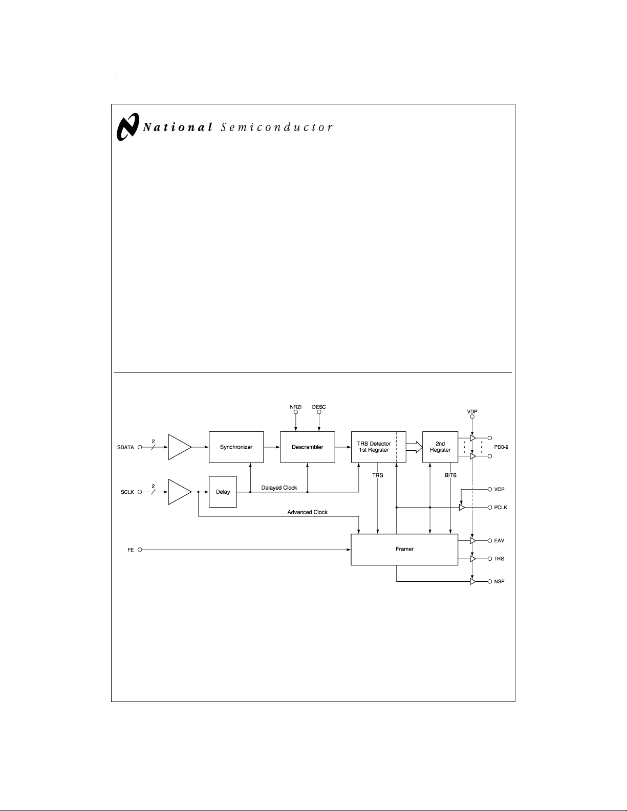
National’s Comlinear CLC011, Serial Digital Video Decoder,
decodes and descrambles SMPTE 259M standard Serial
Digital Videodatastreams with serial clockinto 10-bit parallel
words and a corresponding word-rate clock. SMPTE 259M
standard parallel data is encoded and scrambled using a
9-bit shift register and is also converted from NRZ to NRZI.
The CLC011 restores the original parallel data by reversing
the encoding process. The CLC011 also extracts timing information embedded in the SDV data. These reserved code
words, known as Timing Reference Signals (TRS), indicate
the start and end of each active video line. By decoding the
TRS, the CLC011 correctly identifies the word boundaries of
the encoded input data. Detection of the TRS reserved
codes is indicated by low-true signals at the TRS and End of
Active Video (EAV) outputs.
The CLC011’s design using current-mode logic (CML) reduces noise injection into the power supply thereby easing
board layout and interfacing. The CMOS compatible outputs,
Block Diagram
CLC011 Serial Digital Video Decoder
January 1999
which feature controlled riseand fall times, may be set foreither 3.3V or 5V swings with the VDP and VCP inputs.
The CLC011 Serial Digital Video Decoder, CLC014Adaptive
Cable Equalizer and the CLC016 Data Retiming PLL combine to provide a complete Serial Digital Video receiver system.
The CLC011 is packaged in a 28-pin PLCC.
Features
n Data decoding and deserializing
n CLC011B operates to 360Mbps
n CLC011A operates to 300Mbps
n Low noise injection to power supplies
n Single +5V or −5.2V supply operation
n Output levels programmable for interface to 5V or 3.3V
logic
n Low power
n Low cost
DS100086-1
© 1999 National Semiconductor Corporation DS100086 www.national.com
Page 2
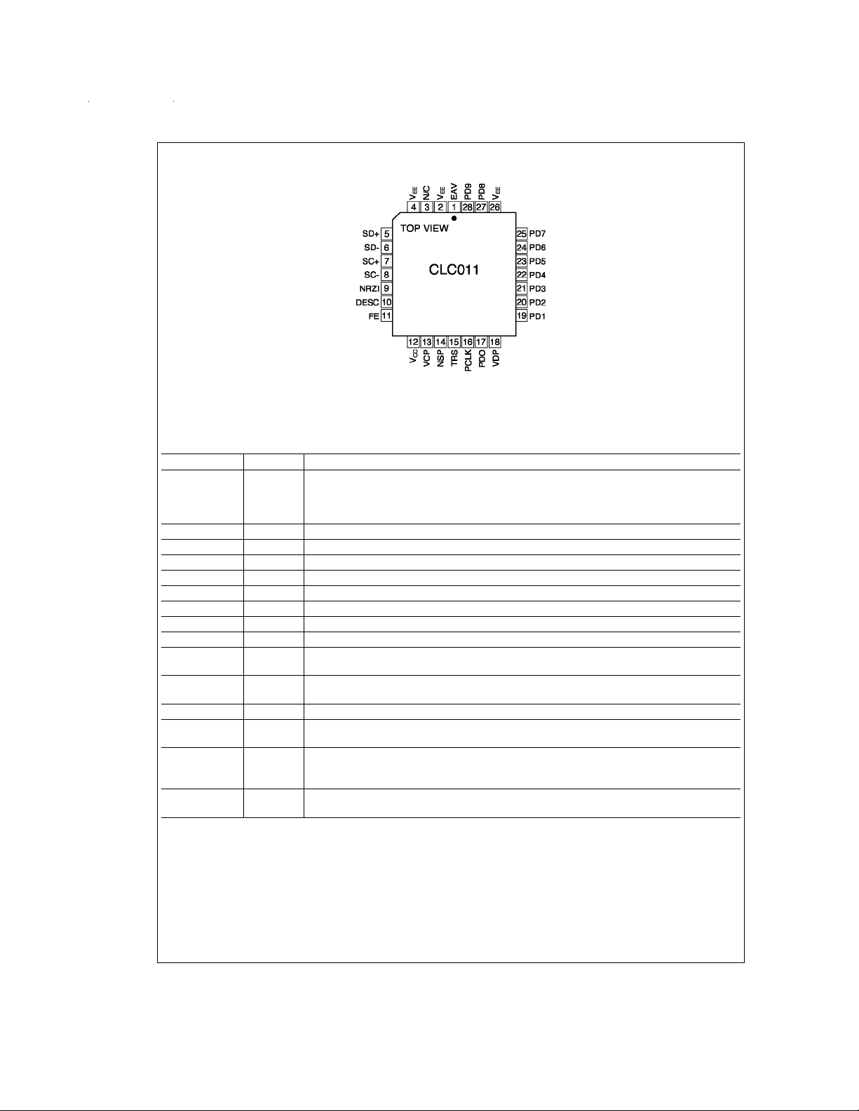
Connection Diagram
DS100086-2
28-Pin PLCC
Order Number CLC011ACQ, or CLC011BCQ
See NS Package Number V28A
Pin Descriptions
Name Pin No. Description
EAV 1 End of active video flag. For component video, a logic low is output for one cycle of the
V
EE
2, 4, 26 Negative supply pins.
NC 3 Unused pin.
SDI+, SDI− 5, 6 Differential serial data inputs.
SCI+, SCI− 7, 8 Differential serial clock inputs.
NRZI 9 A logic high at this pin enables NRZI-to-NRZ conversion.
DESC 10 A logic high at this pin enables descrambling.
FE 11 Frame enable. Enables resynchronization of the parallel word at the next TRS.
V
CC
12 Positive supply pin.
VCP 13 Parallel clock high level programming pin. The voltage at this supply pin defines the logic high
NSP 14 New sync position. Indicates that the most recent TRS is in a new position relative to the
TRS 15 Timing reference flag. A logic low is output for the duration of the TRS.
PCLK 16 Parallel clock output. The rising edge of this clock is located at the center of the parallel data
PD0–9 17,
19–25,
27, 28
VDP 18 Parallel data high level programming pin. The voltage at this supply pin defines the logic high
parallel clock every time an EAV timing reference is detected. The pulse is aligned with the
fourth word of the timing reference (the XYZ word). For composite video, this line is always
asserted high.
level for the parallel clock output.
previous TRS. Remains high until the parallel rate clock is aligned properly with the TRS.
window.
Parallel data outputs.
level for the data outputs.
www.national.com 2
Page 3
Absolute Maximum Ratings (Note 1)
If Military/Aerospace specified devices are required,
please contact the National Semiconductor SalesOffice/
θ
28-Pin PLCC 35˚C/W
JC
Reliability Information
Transistor Count 3076
Distributors for availability and specifications.
Supply Voltage (V
) +6V
CC–VEE
Storage Temperature Range −65˚C to +150˚C
Junction Temperature +150˚C
ESD Rating (HBM)
PDx 500V
other 2kV
Package Thermal Resistance
28-Pin PLCC 85˚C/W
θ
JA
Recommended Operating
Conditions
Supply Voltage (VCC–VEE) 4.5V to 5.5V
Logic High Voltage
(V
Operating Temperature 0˚C to +70˚C
and VDP–VEE) 3.0V to 5.5V
CP–VEE
Electrical Characteristics
(VCC= +5V, VEE= 0V, CL= 10 pF; unless specified).
Parameter Conditions
Typ
+25˚C
Min/Max
+25˚C
DYNAMIC PERFORMANCE
Minimum Serial Data Rate 0 Mbps
Maximum Serial Data Rate CLC011B 400 360 360 Mbps
CLC011A 300 300 Mbps
PDn and PCLK Rise/Fall Time C
PDn and PCLK Rise/Fall Time C
= 2 pF,(Note 9) 2.0 ns
L
= 20 pF,(Note 9) 4.0 ns
L
PCLK Rising Edge Residual Jitter (Note 9) 50 ps
TIMING PERFORMANCE
SD to SC Setup Time 0.2 0.2 ns
SC to SD Hold Time 00ns
PDn to PCLK Skew (Note 9)
PDn Valid to PCLK
PCLK
to PDn Invalid PCLK = 27 MHz, (Note 9) 18 ns
↑
↑
PCLK = 27 MHz, (Note 9) 18 ns
±
0.8 ns
Digital Latency (Notes 6, 7, 9) 42 sclk
Output Buffer Latency (Notes 7, 9) 10 ns
STATIC PERFORMANCE
I
Supply Current (Note 9) VCCPin 44 mA
CC
VDP and VCP Supply Current PCLK = 0 MHz, (Note 9) 2 mA
VDP and VCP Supply Current PCLK = 27 MHz, (Note 9) 12 mA
SD and SC Inputs
Input Range Upper Limit V
Input Range Lower Limit V
EE
Minimum Differential Input 200 200 mV
I
IH
10 15 µA
FE, NRZI, and DESC Inputs
V
IL
V
IH
VEE+0.8 VEE+0.8 V
VEE+2.0 VEE+2.0 V
Outputs
V
OL
V
OH
IOL=10mA VEE+0.5 VEE+0.5 V
IOH=10mA VCC−0.5 VCC−0.5 V
MISCELLANEOUS PERFORMANCE
SD and SC Input Capacitance (Note 9) 2.0 pF
SD and SC Input Resistance (Note 9) 20 kΩ
Note 1: “Absolute Maximum Ratings” are those values beyond which the safety of the device cannot be guaranteed. They are not meant to imply that the devices
should be operated at these limits. The table of “Electrical Characteristics” specifies conditions of device operation.
Min/Max
0˚C to
+70˚C
cycles
CC
V
CC
+2.5 VEE+2.5 V
Units
pp
V
www.national.com3
Page 4

Electrical Characteristics (Continued)
Note 2: Min/Max ratings are based on product characterization and simulation. Individual parameters are tested as noted. Outgoing quality levels are determined
from tested parameters.
Note 3: Nominal position of rising edge of serial clock is at the center of the serial data eye.
Note 4: Nominal position of the rising edge of PCLK is at the center of the PDn eye.
Note 5: See Timing Diagrams.
Note 6: Data latency due to digital registers, measured from MSB of serial data to parallel clock out.
Note 7: Total latency is the digital latency plus the output buffer latency.
Note 8: 100%tested at 25˚C, sample tested over temperature.
Note 9: Typicals only specified.
Timing Diagrams
FIGURE 1.
www.national.com 4
DS100086-3
Page 5

Overview
The CLC011, Serial Digital Video Decoder,decodes and descrambles SMPTE 259M standard Serial Digital Video
datastreams into 10-bit parallel words and a corresponding
word-rate clock. The following information describes:
the CLC011 operation,
•
recommended interface circuitry, and
•
PCB layout suggestions.
•
Applications assistance for the CLC011 may be obtained by
calling the Interface Applications Hotline, (408) 721-8500.
Input Interfacing—Signal Inputs
The serial data and clock inputs of the CLC011 are both differential. Their input voltage ranges from 2.5V above the
negative supply (V
(V
). Supply voltages for the CLC011 may be either +5V or
CC
–5.2V for ECL compatibility and interfacing. When operated
from the negative supply, inputs accept standard ECL signal
levels. The minimum differential input swing is 200 mV. The
CLC011 interfaces with the CLC016 Data Retiming PLL as
shown in
Figure 2
signal inputs appears in
+2.5V) to the positive supply voltage
EE
. A simplified schematic of the CLC011’s
Figure 3
.
DS100086-5
FIGURE 3. Simplified Input Buffer Schematic
Input Interfacing—Control Inputs
Three TTL-compatible inputs control operation of the
CLC011: NRZI, DESC and FE. A typical interface circuit for
the control inputs is shown in
Figure 4
.
FIGURE 2. Interface with CLC016
DS100086-4
DS100086-6
FIGURE 4. Typical Control Logic Connection
NRZI: NRZI, when a logic high, enables NRZI to NRZ con-
version. Forstandard SMPTE 259M operation, NRZI is high.
DESC (Descramble): The bits of a SMPTE 259M
datastream are scrambled upon encoding according to a
polynomial equation. DESC, when a logic high, enables descrambling of the encoded signal. For standard SMPTE
259M operation, DESC is high.
FE (Framing Enable): SMPTE 259M datastreams include a
four-word-long reserved sequence knownas theTiming Reference Signal (TRS). Using this sequence, the CLC011 determines the position of word boundaries, also known as
framing, of the incoming data.
The FE input, when a logic high and following recognition of
a TRS, causes the CLC011 to automatically adjust its framing. The word boundary is aligned at the appropriate bit position and the parallel output clock is aligned with the appropriate cycle of the serial clock. When FE is held low and a
TRS, outof phase withthe current PCLK, is received, output
NSP will gohigh. However,the phase ofPCLK willnot beadjusted. NSP will remain high until a TRS, in-phase with the
current PCLK, is received.
www.national.com5
Page 6

Input Interfacing—Control Inputs
(Continued)
FE is normally conditioned in one of three ways.
1. FE tied high. This is the most common mode for FE. In
this mode, when a TRS is received, PCLK is aligned to
the new TRS. If a new sync position (NSP) is identified,
the NSP output will go high until the next TRS is received.
2. FE tied to NSP. When in this mode, if a TRS that is out
of phase with the existing PCLK is detected, NSP will go
high, but the phase of PCLK will not be adjusted. If the
next TRS received is in-phase with PCLK, NSP will go
low and the decoder will continue without changing its
state. If the next TRSto arriveis outof phase with PCLK,
then PCLK’s phase is adjusted to meet the new TRS
and NSP is made low.Single erroneous TRS pulses are
ignored in this mode, but if they persist, the decoder will
re-adjust PCLK to properly frame the data.
3. FE held low during active video. The automatic framing feature using the TRS may be disabled in cases
where non-SMPTE 259M signals are being processed.
In some applications like computer-generated animation, the serial video data may not adhere to the SMPTE
259M standard and patterns that resemble TSR’s can
occur within the active video line. When such patterns
occur and to prevent the CLC011 from attempting reframing, make FE a logic low during the active video
line.
Output Interface—Output Logic
Levels
All outputs of the CLC011 are CMOS compatible. They can
be programmed to provide appropriate output logic levels to
connect to following stages operating from supplies of 3.0V
to 5.5V. Output voltages areset by applying the positive supply voltage powering the following stage to VDP, which controls PD0-9, EAV, TRS and NSP, and VCP, which controls
PCLK. An example of the CLC011, powered from +5V, driving a device powered from a 3.3V supply is shown in
5
.
Figure
The CLC011’s output drivers, shown simplified in
are designed to maintain a constant, controlled slew rate regardless of load. This design results in lower output switching noiseinjection via the supply pins and into othercircuitry.
Even so, it is recommended that the CLC011 and other digital circuitry be separated from analog circuitry and cable
equalizers.
FIGURE 6. Simplified Output Buffer Schematic
Figure 6
DS100086-8
,
DS100086-7
FIGURE 5. Typical Output Interface
www.national.com 6
Page 7

Output Interface—Control Outputs
PCLK (Parallel Clock): The parallel output or word clock,
PCLK, is synchronous withthe parallel data outputs, PD0–9.
The rising edge of PCLK is located at the center of the parallel data window.
TRS (Timing Reference Signal): The active-low TRS output pulse is four parallel clock periods long. TRS is active
during decoding of both composite and component video
signals.
EAV (End of Active Video): The EAV output is pulsed low
for one cycle of the parallel clock every time an EAV timing
reference is detected during decoding of component video.
The pulse is coincident with the fourth word of the timing reference (the XYZ word).During receptionof composite video,
this output is always asserted high.
NSP (New Sync Position): The active-low NSP output indicates that the most recently received TRSis ina differentposition relative to the previous TRS. NSP remains high until
the parallel rate clock is properly aligned with the TRS, then
goes low.
PCB Layout Guidelines
The CLC011 is not as sensitive to PCB layout as some Serial
Digital Video decoders. The following suggestions will help
achieve and maintain optimum system performance.
1. Locate the CLC011 decoder away from equalizers and
other sensitive circuitry to avoidunwanted crosstalkfrom
clock and data outputs which may degrade system performance.
2. The trace from the signal input connector to the CLC011
must be kept short and should not run parallel to the
data output traces.
3. Bypass each power pin with a 0.01 µF to 0.1 µF monolithic ceramic capacitor.
4. Power the CLC011 and other clock recovery circuitry
from a separate power supply network from that of other
digital circuitry on the board.
Other PCB layout tips may be found in: “KeepingAnalog Signals Pure in a HostileDigital World”, Electronic Design, Special Analog Issue, June 24, 1996, available from National
Semiconductor. Request Literature number 665502-001.
www.national.com7
Page 8

Physical Dimensions inches (millimeters) unless otherwise noted
CLC011 Serial Digital Video Decoder
Order Number CLC011ACQ, or CLC011BCQ
NS Package Number V28A
LIFE SUPPORT POLICY
NATIONAL’S PRODUCTS ARE NOT AUTHORIZED FOR USE AS CRITICAL COMPONENTS IN LIFE SUPPORT DEVICES OR SYSTEMS WITHOUT THE EXPRESS WRITTEN APPROVAL OF THE PRESIDENT OF NATIONAL SEMICONDUCTOR CORPORATION. As used herein:
1. Life support devices or systems are devices or systems which, (a) are intended for surgical implant into
the body, or (b)support or sustain life, andwhose failure to perform when properly used in accordance
2. A critical component is any component of a life support
device or system whose failure to perform can be reasonably expectedto cause the failure of the life support
device or system, or to affect itssafety or effectiveness.
with instructions for use provided in the labeling, can
be reasonably expected to result in asignificant injury
to the user.
National Semiconductor
Corporation
Americas
Tel: 1-800-272-9959
Fax: 1-800-737-7018
Email: support@nsc.com
www.national.com
National does not assume any responsibility for use of any circuitry described, no circuit patent licenses are implied and National reserves the right at any time without notice to change said circuitry and specifications.
National Semiconductor
Europe
Fax: +49 (0) 1 80-530 85 86
Email: europe.support@nsc.com
Deutsch Tel: +49 (0) 1 80-530 85 85
English Tel: +49 (0) 1 80-532 78 32
Français Tel: +49 (0) 1 80-532 93 58
Italiano Tel: +49 (0) 1 80-534 16 80
National Semiconductor
Asia Pacific Customer
Response Group
Tel: 65-2544466
Fax: 65-2504466
Email: sea.support@nsc.com
National Semiconductor
Japan Ltd.
Tel: 81-3-5639-7560
Fax: 81-3-5639-7507
 Loading...