

Page 1
CLC005
ITU-T G.703 Cable Driver with Adjustable Outputs
General Description
National’s Comlinear CLC005 is a monolithic, high-speed
cable driver designed for the ITU-T G.703 serial digital data
transmission standard. The CLC005 drives 75Ω transmission lines (Belden8281 or equivalent) at data rates fromDC
to over 622 Mbps.Outputsignal waveforms produced by the
CLC005 comply with G.703 specifications. Controlled output
rise and fall times (650 ps typical) minimize transitioninduced jitter.The output voltage swing, typically 2.0V, set by
an accurate, low-drift internal bandgap reference, delivers a
1.0V swing to back-matched and terminated 75Ωcable.Output swing is adjustable from 0.7 V
p-p
to 2.2 V
p-p
using exter-
nal resistors.
The CLC005’s class AB output stage consumes less power
than other designs, 185 mW with both outputs terminated,
and requires no external bias resistors. The differential inputs accept a widerange of digital signals from 200mV
p-p
to
G.703 levels within the specified common-mode limits. All
this make the CLC005 an excellent general purpose high
speed driver for digital applications.
The CLC005 is powered from a single +5V or −5.2V supply
and comes in an 8-pin SOIC package.
Key Specifications
n 650 ps rise and fall times
n Data rates to 622 Mbps
n 200 mV differential input
n Low residual jitter (25 ps
pp
)
Features
n No external pull-down resistors
n Adjustable output amplitude
n Differential input and output
n Low power dissipation
n Single +5V or −5.2V supply
Applications
n ITU-T G.703, Sonet/SDH, and ATM compatible driver
n Digital routers and distribution amplifiers
n Coaxial cable driver for digital transmission line
n Twisted pair driver
n Buffer applications
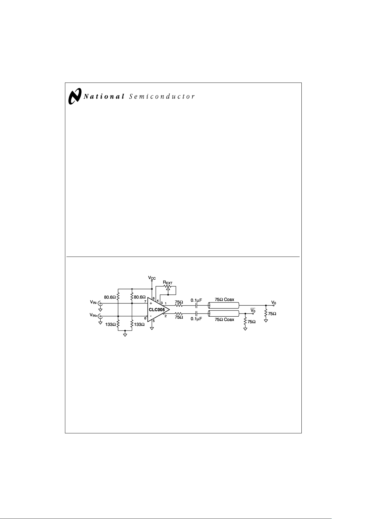
Typical Application
DS100144-2
August 1998
CLC005 ITU-T G.703 Cable Driver with Adjustable Outputs
© 1998 National Semiconductor Corporation DS100144 www.national.com
Page 2
Typical Performance Characteristic
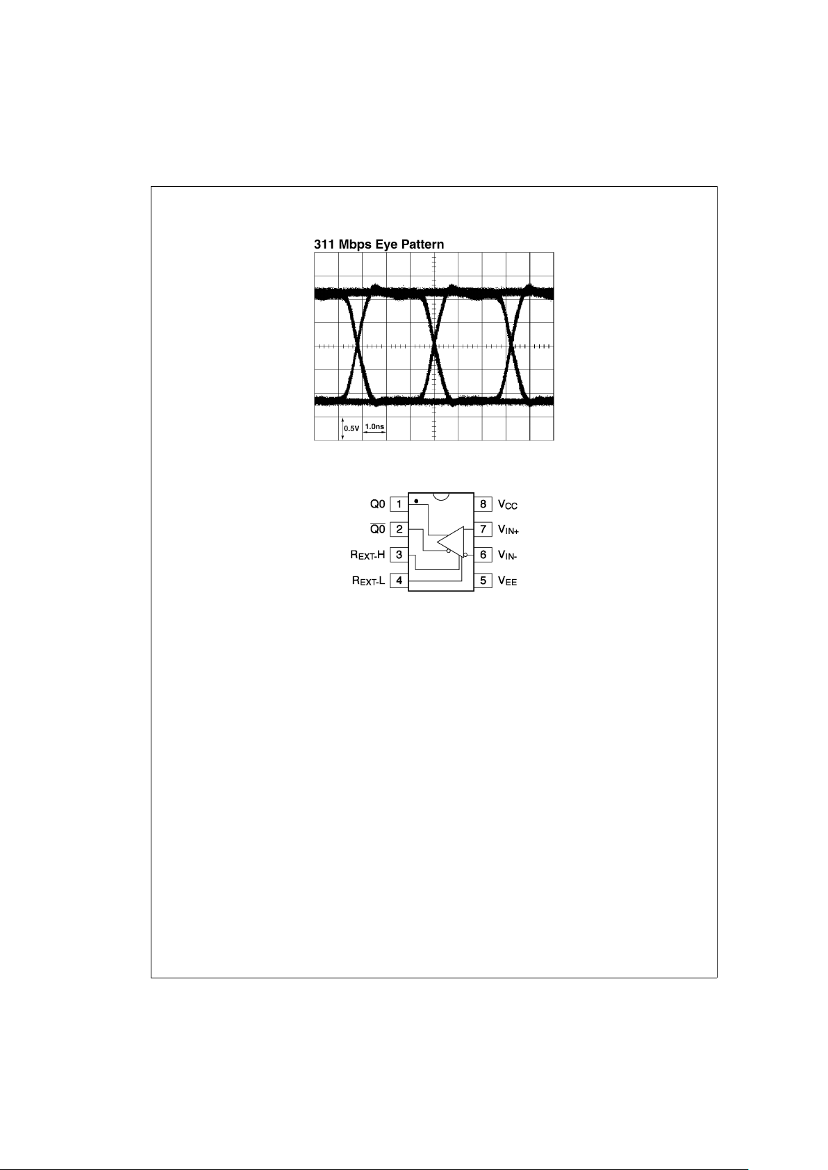
Connection Diagram (8-Pin SOIC)
DS100144-1
DS100144-3
Order Number CLC005AJE
See NS Package Number M08A
www.national.com 2
Page 3
Absolute Maximum Ratings (Note 1)
If Military/Aerospace specified devices are required,
please contact the National Semiconductor Sales Office/
Distributors for availability and specifications.
Supply Voltage 6V
Output Current 30 mA
Maximum Junction Temperature +125˚C
Storage Temperature Range −65˚C to +150˚C
Lead Temperature
(Soldering 10 seconds) +300˚C
ESD Rating (Human Body Model) 1000V
Package Thermal Resistance
θ
JA
Surface Mount AJE 125˚C/W
θ
JC
Surface MountAJE 105˚C/W
Reliability Information
Transistor count 72
MTTF 254 Mhr
Recommended Operating
Conditions
Supply Voltage Range (VCC–VEE) +4.5V to +5.5V
Electrical Characteristics (V
CC
= 0V, VEE= −5V; unless otherwise specified).
Parameter Condition
Typ
+25˚C
Min/Max
+25˚C
Min/Max
0˚C to
+70˚C
Min/Max
-40˚C to
+85˚C
Units
STATIC DC PERFORMANCE
Supply Current, Loaded 150Ω
@
270 Mbps
(Notes 5, 7)
37 - - - mA
Supply Current, Unloaded (Note 3) 34 28/37 26/39 26/39 mA
Output HIGH Voltage (V
OH
) (Note 3) −1.7 −2.0/1.4 −2.0/1.4 −2.0/1.4 V
Output LOW Voltage (V
OL
) (Note 3) −3.7 −4.0/3.4 −4.0/3.4 −4.0/3.4 V
Input Bias Current (Note 4) 10 30 50 50 µA
Output Swing R
EXT
=∞(Note 3) 2.0 1.86/2.14 1.86/2.14 1.86/2.14 V
Output Swing R
EXT
=10kΩ(Note 5) 1.30 - - - V
Common Mode Input Range Upper Limit −0.7 −0.8 −0.8 −0.8 V
Common Mode Input Range Lower Limit −2.6 −2.5 −2.5 –2.5 V
Minimum Differential Input Swing (Note 5) 200 200 200 200 mV
Power Supply Rejection Ratio (Note 3) 26 20 20 20 dB
AC PERFORMANCE
Output Rise and Fall Time (Notes 3, 6, 7) 650 425/825 400/850 400/850 ps
Overshoot (Note 5) 5
%
Propagation Delay (Note 5) 1.0 ns
Duty Cycle Distortion (Note 5) 50 ps
Residual Jitter (Note 5) 25 - - - ps
pp
MISCELLANEOUS PERFORMANCE
Input Capacitance (Note 5) 1.0 pF
Output Resistance (Note 5) 10 Ω
Output Inductance (Note 5) 6 nH
Note 1: “Absolute Maximum Ratings” are those values beyond which the safety of the device cannot be guaranteed. Theyare not meant to imply that the devices
should be operated at these limits. The table of “Electrical Characteristics” specifies conditions of device operation.
Note 2: Min/Max ratings are based on product characterization and simulation. Individual parameters are tested as noted. Outgoing quality levels are determined
from tested parameters.
Note 3: Spec is 100%tested at +25˚C, sample tested at +85˚C.
Note 4: Spec is 100%tested at +35˚C at wafer probe.
Note 5: Spec is guaranteed by design.
Note 6: Measured between the 20%and 80%levels of the waveform.
Note 7: Measured with both outputs driving 150Ω, AC coupled at 270 Mbps.
3 www.national.com
Page 4
Operation
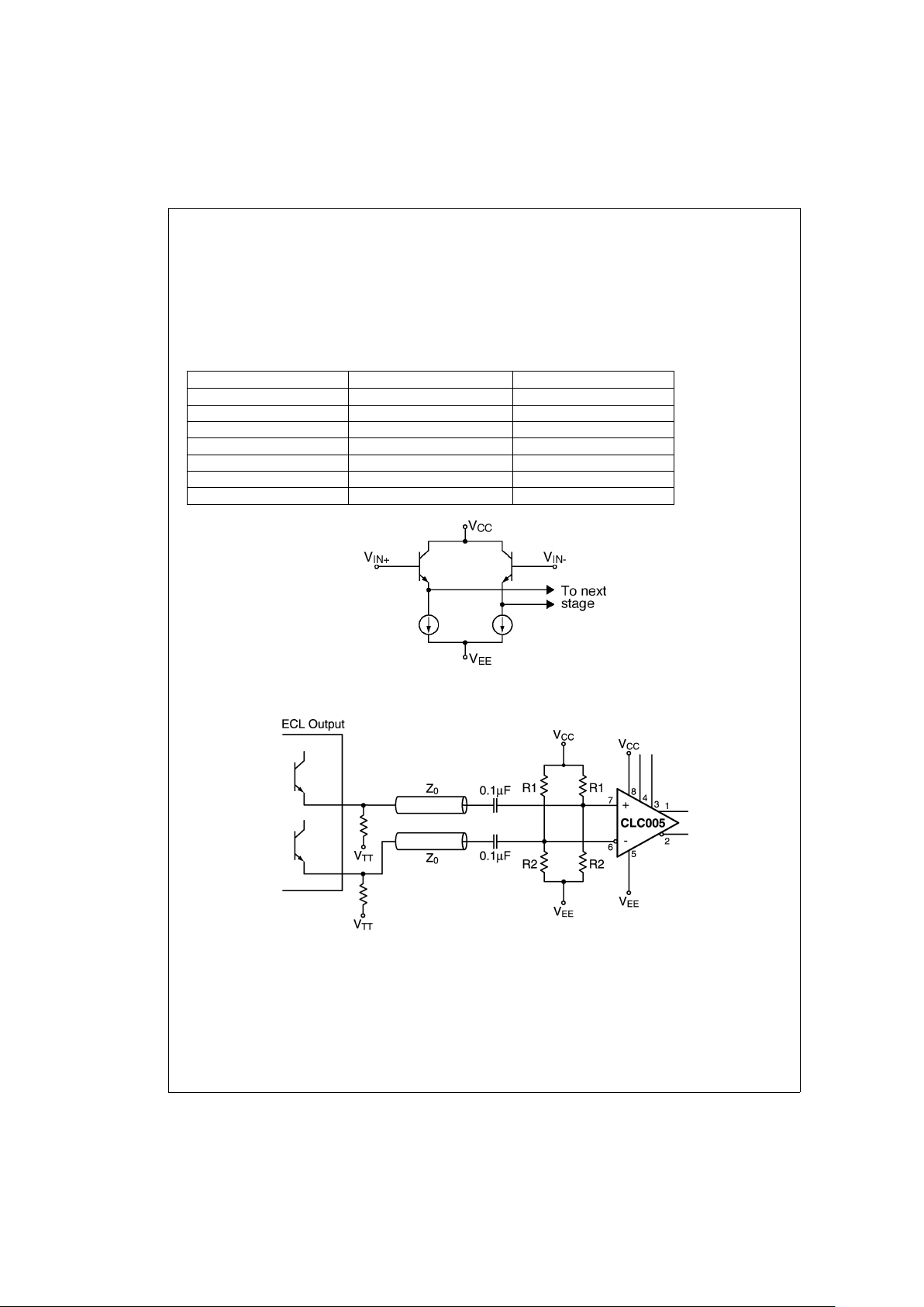
INPUT INTERFACING
The CLC005 has high impedance, emitter-follower buffered,
differential inputs. Single-ended signals may also be input.
Transmission lines supplying input signals must be properly
terminated close to the CLC005. EitherA.C. or D.C. coupling
as in
Figure 2orFigure 3
may be used.
Figures 2, 4
and
Fig-
ure 5
show how Thevenin-equivalent resistor networks are
used to provide input termination and biasing.The input D.C.
common-mode voltage range is 0.8Vto 2.5V belowthe positive power supply (V
CC
). Input signals plus bias should be
kept within the specified common-mode range. For an 800
mV
P-P
input signal, typical input bias levels range from 1.2V
to 2.1V below the positive supply.
Load Type Resistor to VCC(R1) Resistor to VEE(R2)
ECL, 50Ω, 5V, V
T
=2V 82.5Ω 124Ω
ECL, 50Ω, 5.2V, V
T
=2V 80.6Ω 133Ω
ECL, 75Ω, 5V, V
T
=2V 124Ω 187Ω
ECL, 75Ω, 5.2V, V
T
=2V 121Ω 196Ω
800mV
P-P
,50Ω, 5V, VT=1.6V 75.0Ω 154Ω
800mV
P-P
,75Ω, 5V, VT=1.6V 110Ω 232Ω
800mV
P-P
, 2.2KΩ, 5V, VT=1.6V 3240Ω 6810Ω
DS100144-4
FIGURE 1. Input Stage
DS100144-5
FIGURE 2. AC Coupled Input
www.national.com 4
Page 5

Operation (Continued)
OUTPUT INTERFACING
The CLC005’s class AB output stage,
Figure 6
, requires no
standing current in the output transistors and therefore requires no biasing or pull-down resistors. Advantages of this
arrangement are lowerpower dissipation and fewer external
components. The outputmay be either D.C. orA.C. coupled
to the load. A bandgap voltagereference sets output voltage
levels which are compatible with F100K and 10K ECL when
correctly terminated. Theoutputs do not have the same output voltage temperature coefficient as 10K. Therefore, noise
margins will be reduced over the full temperature range
when driving 10K ECL. Noise margins will not be affected
when interfacing to F100K since F100K is fully voltage and
temperature compensated.
DS100144-6
FIGURE 3. DC Coupled Input
DS100144-7
FIGURE 4. Single Ended 50Ω ECL Input
DS100144-8
FIGURE 5. Differential 50Ω ECL Input
DS100144-9
FIGURE 6. Output Stage
5 www.national.com
Page 6

Operation (Continued)
OUTPUT AMPLITUDE ADJUSTMENT
The high and low output levels of the CLC005 are set by a
circuit shown simplifiedin
Figure 8
. Output highand low levels may be setindependently withexternal resistornetworks
connected between R
EXT-H
(pin 3), R
EXT-L
(pin 4) and the
power supplies. The resistor networks affect the high and
low output levels by changing the internally generated bias
voltages, V
H
and VL. The nominal high and low output levels
are V
CC
−1.7V and VCC−3.7V, respectively, when the pins
R
EXT-H
and R
EXT-L
are left unconnected. Thoughthe internal
components which determine output voltage levels have accurate ratios, their absolute values may be controlled only
within about
±
15%of nominal. Even so,without externaladjustment, output voltages are well controlled. A final design
should accommodate the variation in externally set output
voltages due to the CLC005’s part-to-part and external component tolerances.
Output voltage swingmay be reduced with thecircuit shown
in
Figure 9
. A single resistance chosen with the aid of the
graph,
Figure 10
, is connected between pins 3and 4. Output
voltage swing may be increased with the circuit of
Figure 11
.
Figure 12
is used to estimate a value forresistor R. Notethat
both of these circuits and the accompanying graphs assume
that the CLC005 is loaded with the standard150Ω. Be aware
that output loading will affect the output swing and the high
and low levels. It may be necessary to empirically select resistances used to setoutput levelswhen theD.C. loadingon
the CLC005 differs appreciably from 150Ω.
DS100144-10
FIGURE 7. Differential Input DC Coupled Output
DS100144-11
FIGURE 8. Equivalent Bias Generation Circuit
www.national.com 6
Page 7

Operation (Continued)
DS100144-12
FIGURE 9. Differential Input Reduced Output
DS100144-13
FIGURE 10. Resistance Pins 3 to 4 vs Output Voltage
Reduced Output
@
150Ω Load
DS100144-14
FIGURE 11. Differential Input Increased Output
7 www.national.com
Page 8

Operation (Continued)
OUTPUT RISE AND FALL TIMES
Output load capacitance can significantly affect output rise
and fall times.The effect of load capacitance, stray or otherwise, may be reduced by placing the output back-match resistor close to the output pin and by minimizing all interconnecting trace lengths.
Figure 13
shows the effect onrisetime
of parallel load capacitance across a 150Ω load.
DS100144-15
FIGURE 12. Resistance Pins 3 to 4 vs Output Voltage
Increased Output
@
150Ω Load
DS100144-16
FIGURE 13. Rise Time vs C
L
www.national.com 8
Page 9

PCB Layout Recommendations
Printed circuit board layout affects the performance of the
CLC005. The following guidelines will aid in achieving satisfactory device performance.
•
Use a ground plane or power/ground plane sandwich design for optimum performance.
•
Bypass device power with a 0.01 µF monolithic ceramic
capacitor in parallel with a 6.8 µFtantalum electrolytic capacitor located no more than 0.1″ (2.5 mm) from the device power pins.
•
Provide short, symmetrical ground return paths for:
— inputs,
— supply bypass capacitors and
— the output load.
•
Provide short, grounded guard traces located
— under the centerline of the package,
— 0.1″ (2.5 mm) from the package pins
— on both top and bottom of the board with connecting
vias.
EVALUATION BOARD
A schematic, parts list and layout for a suitable evaluation
board are given on the following page. The artwork includes
trace, silk screen and ground layers. The individual printed
circuit board is available unassembled from National Semiconductor. To order this evaluation board, part number
CLC730056, contact your local sales representative or
the National Semiconductor Customer Response Center
in your area. (This evaluation board is identical to that for
the CLC007 for which some of the listed parts are not required.)
The evaluation board is a guide to proper circuit layout and
makes prototyping and measurement-taking easy. Since the
board is designed to accommodate many of the application
circuits possible with theCLC005, yourparticular application
may not require allof thelisted partsor mayrequire different
values. The evaluation board may be powered from standard
ECL supply voltages by installing the two jumpers in the locations labeled “−5”. For PECL supply voltages, install the
jumpers in the locations labeled “+5”.
DS100144-17
CLC005 Evaluation Board Schematic
9 www.national.com
Page 10

PCB Layout Recommendations (Continued)
Item Reference Designator Part Description Qty
1 C1, C2, C8, C9 0.1 µF SMD Capacitor, Size 1206 4
2 C5, C60 33 pF SMD Capacitor, Size 1206 2
3 C7, C10, C13, C14 0.01 µF SMD Tantalum Capacitor, Size 12062 4
4 C11, C12 6.8 µF SMD Tantalum Capacitor, Size 6032 2
5 J1, J2 BNC PC Amphenol #31-5329-52RFX 2
6 J3, J4 BNC PC Amphenol #31-5329-72RFX 2
7 R3, R1 124Ω SMD Resistor, Size 1206 2
8 R4, R5 82.5Ω SMD Resistor, Size 1206 2
9 R6,R7 75Ω SMD Resistor, Size 1206 2
10 R11 2.4 kΩ SMD Resistor, Size 1206 1
11 R12 3 kΩ SMD Resistor, Size 1206 1
12 U1 CLC005AJE Cable Driver 1
13 +5, −5 Jumper 4
14 VR1 10 kΩ Potentiometer, Bourns 3299 1
www.national.com 10
Page 11

PCB Layout Recommendations (Continued)
DS100144-18 DS100144-19
DS100144-20
DS100144-21
11 www.national.com
Page 12

Physical Dimensions inches (millimeters) unless otherwise noted
LIFE SUPPORT POLICY
NATIONAL’S PRODUCTS ARE NOT AUTHORIZED FOR USE AS CRITICAL COMPONENTS IN LIFE SUPPORT DEVICES OR SYSTEMS WITHOUT THE EXPRESS WRITTEN APPROVAL OF THE PRESIDENT OF NATIONAL SEMICONDUCTOR CORPORATION. As used herein:
1. Life support devices or systems are devices or systems which, (a) are intended for surgical implant into
the body, or (b) supportor sustain life,and whose failure to perform when properly used in accordance
with instructions for use provided in the labeling, can
be reasonably expected to resultin a significantinjury
to the user.
2. A critical component in any component of a life support
device or system whose failure to perform can be reasonably expected to causethe failureof the life support
device or system, or toaffect its safetyor effectiveness.
National Semiconductor
Corporation
Americas
Tel: 1-800-272-9959
Fax: 1-800-737-7018
Email: support@nsc.com
www.national.com
National Semiconductor
Europe
Fax: +49 (0) 1 80-530 85 86
Email: europe.support@nsc.com
Deutsch Tel: +49 (0) 1 80-530 85 85
English Tel: +49 (0) 1 80-532 78 32
Français Tel: +49 (0) 1 80-532 93 58
Italiano Tel: +49 (0) 1 80-534 16 80
National Semiconductor
Asia Pacific Customer
Response Group
Tel: 65-2544466
Fax: 65-2504466
Email: sea.support@nsc.com
National Semiconductor
Japan Ltd.
Tel: 81-3-5620-6175
Fax: 81-3-5620-6179
Order Number CLC005AJE
NS Package Number M08A
CLC005 ITU-T G.703 Cable Driver with Adjustable Outputs
National does not assume any responsibility for use of any circuitry described, no circuit patent licenses are implied and National reserves the right at any time without notice to change said circuitry and specifications.
 Loading...