

Page 1
CLC001
Serial Digital Cable Driver with Adjustable Outputs
General Description
The CLC001 is a monolithic, high-speed cable driver
designed for use in SMPTE 259M serial digital video and
ITU-T G.703 serial digital data transmission applications.
The CLC001 drives 75Ω transmission lines (Belden 8281 or
equivalent) at data rates up to 622 Mbps. Controlled output
rise and fall times (400 ps typical) minimize transitioninduced jitter. The output voltage swing is adjustable from
800 mV
p-p
to 1.0 V
p-p
using an external resistor.
The CLC001’soutput stage consumes less power than other
designs. The differential inputs accept LVDS signal levels,
LVPECL levels directly or PECL with attenuation networks.
All these make the CLC001 an excellent general purpose
high speed driver for high-speed, long distance data
transmission applications.
The CLC001 is powered from a single +3.3V supply and
comes in a small 8-pin SOIC package.
Key Specifications
n 400 ps rise and fall times
n Data rates to 622 Mbps
n 100 mV differential input threshold
n Low residual jitter
Features
n Adjustable output amplitude
n Differential input and output
n Accepts LVPECL or LVDS input swings
n Low power dissipation
n Single +3.3V supply
Applications
n Digital routers and distribution amplifiers
n Coaxial cable driver for digital transmission lines
n Twisted pair driver
n Serial digital video interfaces for the commercial and
broadcast industry
n SMPTE, Sonet/SDH, and ATM compatible driver
n Buffer applications
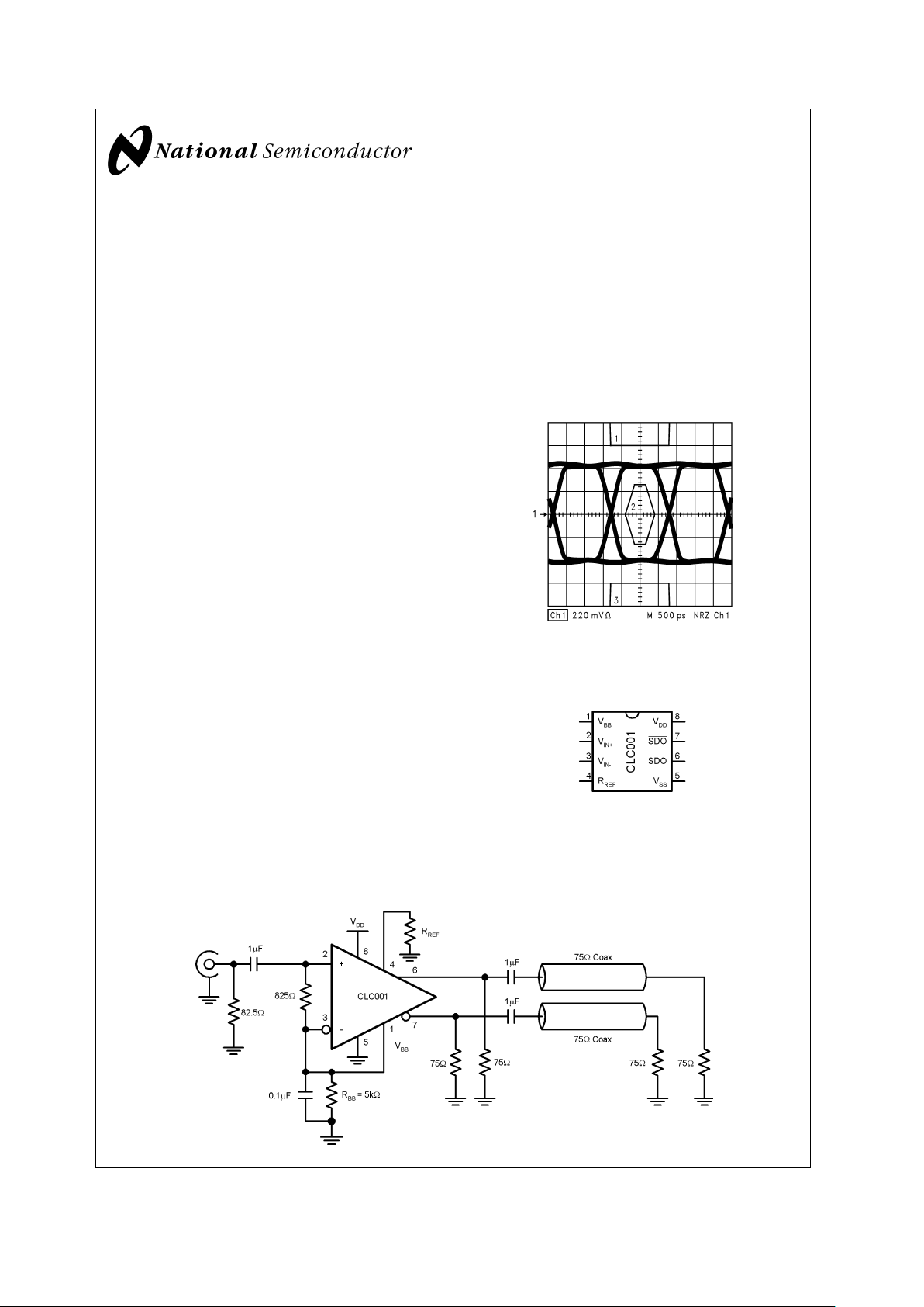
Connection Diagram (8-Pin SOIC)
Typical Application
DS101329-10
622 Mbps Eye Pattern with STM-4 Signal Mask
DS101329-2
Order Number CLC001AJE
See NS Package Number M08A
DS101329-1
March 2001
CLC001 Serial Digital Cable Driver with Adjustable Outputs
© 2001 National Semiconductor Corporation DS101329 www.national.com
Page 2
Absolute Maximum Ratings (Note 1)
If Military/Aerospace specified devices are required,
please contact the National Semiconductor Sales
Office/Distributors for availability and specifications.
Supply Voltage 4V
Output Current 27 mA
Maximum Junction Temperature +125˚C
Storage Temperature Range −65˚C to +150˚C
Lead Temperature
(Soldering 10 seconds) +300˚C
ESD Rating (HBM) ≥ 7kV
ESD Rating (MM) ≥ 500V
Package Thermal Resistance
θ
JA
Surface Mount AJE 125˚C/W
θ
JC
Surface Mount AJE 105˚C/W
Reliability Information
Transistor count 291
Recommended Operating
Conditions
Supply Voltage Range (VDD-VSS) +3.0V to +3.6V
Operating Free Air Temperature (T
A
) -40˚C to +85˚C
R
BB
Range (applied to VBBinput)
(Note 6) 1.3kΩ to 11.5kΩ
Electrical Characteristics
Over recommended operating supply and temperature ranges unless otherwise specified (Notes 2 and 3)
Symbol Parameter Conditions Min Typ Max Units
OUTPUT DC SPECIFICATIONS
V
SDO
Serial Driver Output Voltage RL=75Ω1%,
R
REF
= 1.91 kΩ 1% (for 800 mV
p-p
),
Figure 1
720 800 880 mV
R
L
=75Ω1%,
R
REF
= 1.5 kΩ 1% (for 1.0 V
p-p
),
Figure 1
900 1000 1100 mV
INPUT DC SPECIFICATIONS
V
TH
Differential Input High Threshold VCM= +0.05V or +1.2V or +3.25V, 0 +100 mV
V
TL
Differential Input Low Threshold VDD= 3.3V −100 0 mV
V
CMR
Common Mode Voltage Range VID= 100mV, VDD= 3.3V 0.05 3.25 V
I
IN
Input Current VIN= 0V or +3.0V, VDD= 3.6V or 0V
±
1
±
10 µA
I
INB
Input Current Balance VIN= 0V or +3.0V, VDD= 3.6V or 0V,
(Note 8)
0.23 µA
SUPPLY CURRENT
I
DD
Total Dynamic Power Supply Current
(includes load current)
RL=75Ω,
R
REF
= 1.91 kΩ 1%
(V
SDO
= 800 mV
p-p
@
270 Mbps)
70 115 mA
R
L
=75Ω,
R
REF
= 1.5 kΩ 1%
(V
SDO
= 1.0 V
p-p
@
622 Mbps)
85 130 mA
MISCELLANEOUS PARAMETERS
L
GEN
Output Inductance 6nH
R
GEN
Output Resistance 25 kΩ
I
BB
VBBCurrent R
REF
= 1.91 kΩ 1%, (Note 6) 250 µA
R
REF
= 1.5 kΩ 1%, (Note 6) 315 µA
CLC001
www.national.com 2
Page 3
AC Electrical Characteristics
Over recommended operating supply and temperature ranges unless otherwise specified (Note 3)
Symbol Parameter Conditions Min Typ Max Units
t
r,tf
Rise time, Fall time 20%–80%, (Notes 4, 5) 400 800 ps
t
os
Output overshoot 5%
t
jit
Output jitter (Note 7) 25 ps
t
pd
Propagation delay (Note 5) 1.9 ns
Note 1: “Absolute Maximum Ratings” are those values beyond which the safety of the device cannot be guaranteed. They are not meant to imply that the devices
should be operated at these limits. The table of “Electrical Characteristics” specifies conditions of device operation.
Note 2: Current flow into device pins is defined as positive. Current flow out of device pins is defined as negative. All voltages are stated referenced to V
SS
=0V.
Note 3: Typical values are at 25˚C and 3.3V.
Note 4: This parameter is Guaranteed by Design.
Note 5: R
L
=75Ω, AC-coupled at 270 Mbps, R
REF
= 1.91 kΩ 1% (for V
SDO
= 800 mV
p-p
±
10%), CLnot greater than 5pF (See
Figure 1
)
Note 6: The V
BB
output is intended as a bias supply pin for the inputs of this device only. It is not designed as a power supply output and should not be used to
power other devices.
Note 7: R
L
=75Ω, AC-coupled at 622 Mbps, R
REF
= 1.5 kΩ 1% (for V
SDO
= 1.0 V
p-p
±
10%), clock pattern input.
Note 8: Input Current Balance (I
INB
) is the difference between the Input Current (IIN)onV
IN+
and V
IN−
for the same bias condition.
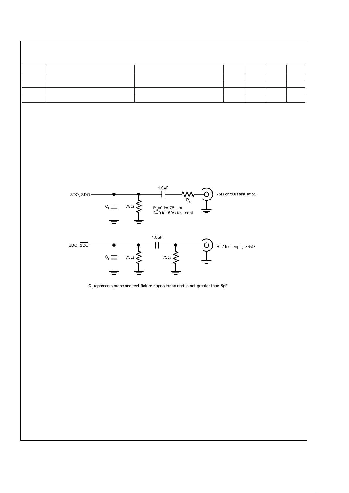
Test Loads
DS101329-4
FIGURE 1. Test Loads
CLC001
www.national.com3
Page 4

Test Loads (Continued)
Pin Descriptions
Pin # Name Description
1V
BB
Optional, bias voltage (may be used to bias inputs) - see device operation
section for details. If unused leave as no connect (NC).
2V
IN+
Positive input pin
3V
IN-
Negative input pin
4R
REF
Output driver level control. Connect a resistor to ground to set output voltage
swing.
5V
SS
Negative power supply
6 SDO Serial data true output
7 SDO
Serial data complement output
8V
DD
Positive power supply
DS101329-3
FIGURE 2. Test Circuit
CLC001
www.national.com 4
Page 5

Device Operation
INPUT INTERFACING
Numerous input configurations exist for applying PECL,
LVPECL, and LVDS signals to the input of the CLC001.
Inputs may be single-ended or differential, AC or DC
coupled.
The V
BB
pin may be used to provide a DC bias voltage to
the inputs. Leave this pin as a no connect when no bias is
needed. Note that DC-coupled inputs such as direct
LVDS and LVPECL connections are self-biasing and do
not require use of the V
BB
pin. IBB, the current produced
by the V
BB
pin, depends on R
REF
. For a given R
REF
, the
I
BB
current will remain constant, and the bias voltage is
determined by the value of resistance, R
BB
, between the
V
BB
pin and ground.
Figure 3
and
Figure 4
show how R
BB
corresponds to some common VBBvalues with R
REF
held
at 1.91 kΩ and 1.5 kΩ, respectively.Some common input
configurations are shown in
Figure 5
through
Figure 9
.
DS101329-11
FIGURE 3. RBBvs. VBBfor R
REF
= 1.91 kΩ
DS101329-12
FIGURE 4. RBBvs. VBBfor R
REF
= 1.5 kΩ
CLC001
www.national.com5
Page 6

Device Operation (Continued)
Figure 5
shows the CLC001 with an AC-coupled, single
ended input connection. The 82.5Ω resister in parallel
with 825Ω gives the equivalent termination resistance of
75Ω.R
BB
set at 5kΩ provides 1.25V of DC bias to the
input.
A typical DC-coupled, twisted pair cable connection is
shown in
Figure 6
. The CLC001 is driven differentially.
The line is terminated with a termination resistor equal to
the impedance of the linebeing driven. The actual resistor
value is media specific, but typically is between 100 and
120Ω depending upon the cable. This resistor should be
located close to the CLC001 inputs pins to minimize the
resulting stub length between the resistor and device
pads.
DS101329-5
FIGURE 5. Single Ended 75Ω Coaxial Cable, AC-coupled
DS101329-6
FIGURE 6. Twisted Pair Cable, DC-coupled
CLC001
www.national.com 6
Page 7

Device Operation (Continued)
Figure 7
shows an AC-coupled, twisted pair cable
application. It implements a center tap capacitance
termination used in conjunction with two 50Ω resistors to
filter common mode noise. R
BB
set at 5kΩ provides 1.25V
of DC bias to each input.
PECL or LVPECL drivers may be interfaced to the
CLC001 as shown in
Figure 8
. The voltage divider
network will reduce the PECL output to the proper levels.
For LVPECL, the 100Ω series resistors should be
removed, since the common mode range inputs of the
CLC001 are wide enough to accept LVPECL levels
directly. No external DC biasing is required for
PECL/LVPECL connections.
DS101329-7
FIGURE 7. Twisted Pair Cable, AC-coupled
DS101329-8
FIGURE 8. PECL, DC-coupled
CLC001
www.national.com7
Page 8

Device Operation (Continued)
Atypical LVDS input connection is shown in
Figure 9
. The
media is driven differentially by an LVDS driver.The line is
terminated with a termination resistor equal to the
impedance of the line being driven. The actual resistor
value is media specific, but typically is between 100 and
120Ω. This resistor should be located close to the
CLC001 inputs pins to minimize the resulting stub length
between the resistor and device pads. The CLC001
supports
±
100mV thresholds across the entire LVDS
common mode range of 0.1V to 2.3V for a 200mV
differential signal.
DS101329-9
FIGURE 9. LVDS, DC-coupled
CLC001
www.national.com 8
Page 9

Device Operation (Continued)
OUTPUT INTERFACING
The CLC001 has two complementary, ground referenced
outputs designed to drive AC-coupled and terminated
75Ω coaxial cables. The outputs are single ended;
however, they could be treated as a single differential
output as long as current paths from each output go to
ground.
The output of the CLC001 is a high impedance current
source. It expects to see a 75Ω shunt resistor before
driving cable to convert the current output to a voltage
and provide proper back-matching. No series backmatching resistors should be used. Refer to
Typical
Application
for an illustration.
Output levels range from 800 mV
p-p
to 1.0 V
p-p
±
10% into
75Ω AC-coupled, back-matched loads. Output level is
controlled by the value of R
REF
connected to pin 4. R
REF
is 1.91 kΩ±1% for 800 mV
p-p
, and 1.5 kΩ±1% for 1.0
V
p-p
. Refer to
Figure 10
for the output level’s sensitivity to
R
REF
.
The CLC001 is designed as an AC-coupled 75Ω cable
driver. It is not intended to drive 50Ω loads. The current
source output does not provide enough current to allow
for 800mV across a 50Ω doubly terminated load.
Evaluation Board
Evaluation boards are available for a nominal charge that
demonstrate the basic operation of the SDI/SDV/SDH
devices. The evaluation boards can be ordered through
National’s Distributors. Supplies are limited, please check for
current availability.
The SD001EVK evaluation kit for the CLC001, Serial Digital
Cable Driver with Adjustable Outputs, provides an operating
environment in which the cable driver can be evaluated by
system / hardware designers. The evaluation board has all
the needed circuitry and connectors for easy connection and
checkout of the device circuit options as discussed in the
CLC001 datasheet. A schematic, parts list and pictorial
drawing are provided with the board.
From the WWW, the following information may be viewed /
downloaded for most evaluation boards:
www.national.com/appinfo/interface
•
Device Datasheet and / or EVK User Manual
•
View a picture of the EVK
•
View the EVK Schematic
•
View the top assembly drawing and BOM
•
View the bottom assembly drawing and BOM
PCB Layout Recommendations
Printed circuit board layout affects the performance of the
CLC001. The following guidelines will aid in achieving
satisfactory device performance.
•
Use a ground plane or power/ground plane sandwich
design for optimum performance.
•
Bypass device power with a 0.01 µF monolithic ceramic
capacitor in parallel with a 6.8 µF tantalum electrolytic
capacitor located no more than 0.1″ (2.5 mm) from the
device power pins.
•
Provide short, symmetrical ground return paths for:
— inputs,
— supply bypass capacitors and
— the output load.
•
Provide short, grounded guard traces located
— under the centerline of the package,
— 0.1″ (2.5 mm) from the package pins
— on both top and bottom of the board with connecting
vias.
DS101329-13
FIGURE 10. Output level’s sensitivity to R
REF
CLC001
www.national.com9
Page 10

Physical Dimensions inches (millimeters) unless otherwise noted
LIFE SUPPORT POLICY
NATIONAL’S PRODUCTS ARE NOT AUTHORIZED FOR USE AS CRITICAL COMPONENTS IN LIFE SUPPORT
DEVICES OR SYSTEMS WITHOUT THE EXPRESS WRITTEN APPROVAL OF THE PRESIDENT AND GENERAL
COUNSEL OF NATIONAL SEMICONDUCTOR CORPORATION. As used herein:
1. Life support devices or systems are devices or
systems which, (a) are intended for surgical implant
into the body, or (b) support or sustain life, and
whose failure to perform when properly used in
accordance with instructions for use provided in the
labeling, can be reasonably expected to result in a
significant injury to the user.
2. A critical component is any component of a life
support device or system whose failure to perform
can be reasonably expected to cause the failure of
the life support device or system, or to affect its
safety or effectiveness.
National Semiconductor
Corporation
Americas
Tel: 1-800-272-9959
Fax: 1-800-737-7018
Email: support@nsc.com
National Semiconductor
Europe
Fax: +49 (0) 180-530 85 86
Email: europe.support@nsc.com
Deutsch Tel: +49 (0) 69 9508 6208
English Tel: +44 (0) 870 24 0 2171
Français Tel: +33 (0) 1 41 91 8790
National Semiconductor
Asia Pacific Customer
Response Group
Tel: 65-2544466
Fax: 65-2504466
Email: ap.support@nsc.com
National Semiconductor
Japan Ltd.
Tel: 81-3-5639-7560
Fax: 81-3-5639-7507
www.national.com
Order Number CLC001AJE
NS Package Number M08A
CLC001 Serial Digital Cable Driver with Adjustable Outputs
National does not assume any responsibility for use of any circuitry described, no circuit patent licenses are implied and National reserves the right at any time without notice to change said circuitry and specifications.
 Loading...