

Page 1
CORPORATION
1.25VPrecision Adjustable
Shunt Reference / Amplifier
Preliminary Product Information
CL432
FEATURES
•• T emperatur e- Co m p ensated: 50ppm/
o
C
•• Trimmed 0.5% Bandgap Reference
•• Internal Amplifier with 150mA Capability
•• Nominal Temperature Range Extended to 105
o
C
•• Low Frequenc y Dynami c Output Imp edan ce: < 150m
•• Low Output Noise
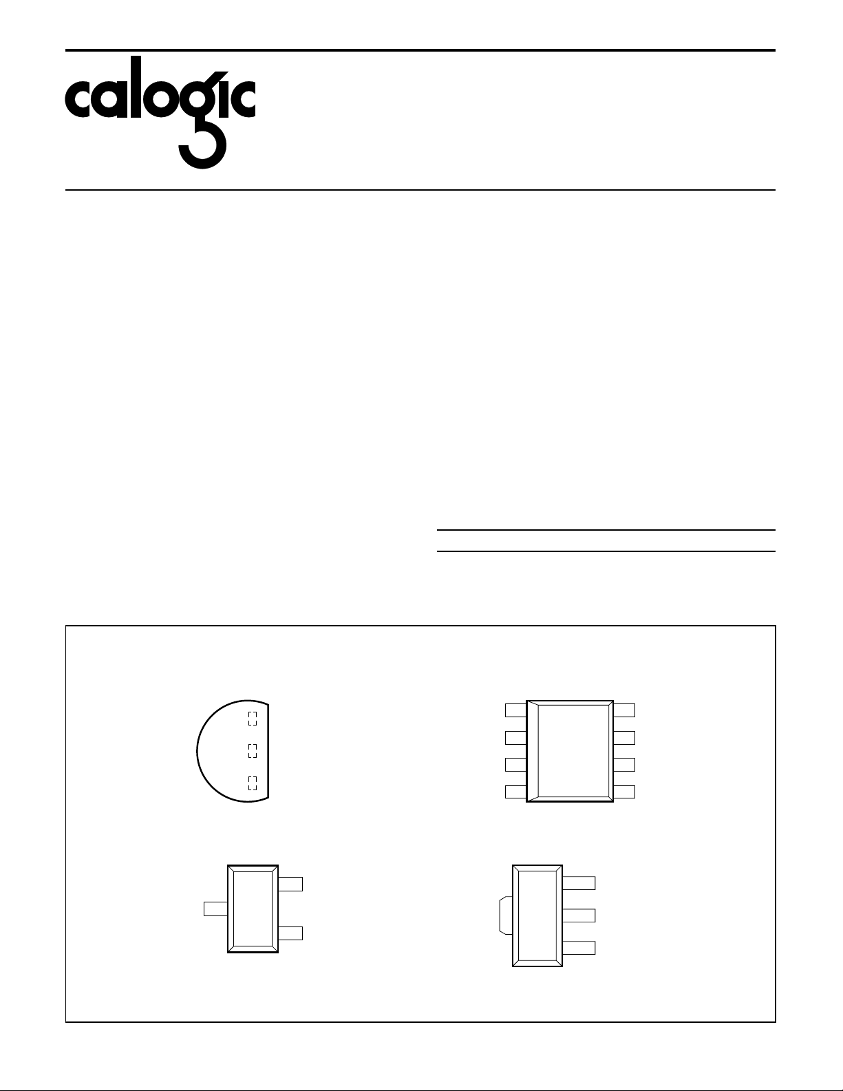
PIN CONFIGU R ATIO N (Top View)
DESCRIPTION
Calogic’s CL432 is a 3-terminal Adjustable Shunt Regulator
highly accurate 1.25V bandgap reference with a 0.5%
tolerance. The device offers thermal stability, wide operating
current (100mA) and an extended temperature range of 0
o
C for operation in power supply applications. The CL432
105
o
to
offers a wide operating voltage range of up to 18V and is an
excellent choice for voltage reference requirements in an
isolated feedback circuit for 3.0V to 3.3V switching mode
power supplies. The tight tolerance guarantees a lower
design cost for the power supply manufacturer by virtually
eliminating the need for an extra power supply manufacturing
process of the power supply.
The device is housed in several package options to meet the
designers crite ria.
ORDERING INFORMATION
Part Package Temperature Range
o
CL432LP TO-92 0 to 105
CL432D 8-Pin Plastic SOI C 0 to 105
CL432VS SOT-23 0 to 105
CL432S SOT-89 0 to 105
C
o
C
o
C
o
C
ANODE
TO-92 (LP)
SOT-23 (VS)
CATHODE
ANODE
REFERENCE
1G-33
CATHODE
REFERENCE
CATHODE
ANODE
ANODE
N/C
1J-22
1
2
3
4
SOT-89 (S)
SOIC (D)
8
REFERENCE
7
ANODE
6
ANODE
5
N/C
CATHODE
ANODE
REFERENCE
1G-35
1G-34
CALOG IC CORPOR ATION, 237 Whitney Place, Fremont, California 94539, Telephone: 510-656-2900, FAX: 510-651-3025
Page 2
CL432
CORPORATION
ABSOLUTE MAXIMUM RATINGS
SYMBOL PARAMETER RATING UNITS
V
KA
I
AK
I
KA
I
REF
P
D
T
J
T
STG
T
L
Stresses greater than those listed under ABSOLUTE MAXIMUM RATINGS may cause permane nt damag e to the device. This is a stress r ating
only and functional operation of the device at these or any other conditions above those indicated in the operational sections of this specification
is not implied. Exposure to ab solut e ma ximu m rati ng conditi on s for ext ende d peri od s may affe ct reliab ili ty.
RECOMMENDED CONDITIONS
SYMBOL P ARAMETER RATING UNIT
V
KA
I
K
Cathode-Anode Reverse Breakdown 18 V
Anode-Cathode Forward Current 1 A
Operating Cathode Current 100 mA
Reference Inp ut Current 1 mA
Continuou s Power at 25oC
TO-92
8L SOIC
SOT-23
SOT-89
775
750
1000
200
Junction Temperature 150
Storage Temperature –65 to 150
Lead Temperature, Soldering 10 Seconds 300
TYPICAL THERMAL RESISTANCES
Cathode Voltage V
to 18 V
REF
Cathode Current 10 mA
PACKAGE θ
TO-92 160
SOIC 175
SOT-23 575
SOT-89 110
JA
o
C/W 80oC/W 6.3mW/oC
o
C/W 45oC/W 5.7mW/oC
o
C/W 150oC/W 1.7mW/oC
o
C/W 8oC/W 9.1mW/oC
θ
JC
mW
mW
mW
mW
o
C
o
C
o
C
TYPICAL DERATING
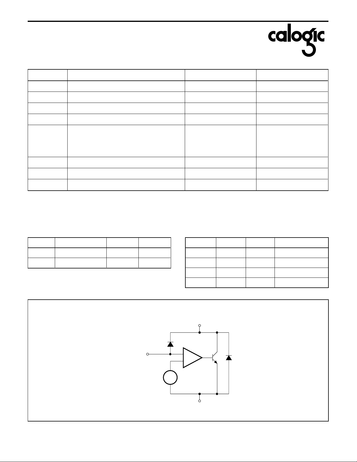
FUNCTIONAL BLOCK DIAGRAM
CATHODE (K)
REFERENCE (R)
+
–
+
1.25V
–
ANODE (A)
1J-23
CALOG IC CORPOR ATION, 237 Whitney Place, Fremont, California 94539, Telephone: 510-656-2900, FAX: 510-651-3025
Page 3
CL432
CORPORATION
ELECTRICAL CHARACTERISTICS
Electrica l characte ri stics are gua ran te ed over full junction temp erature range (0 to 105oC). Ambient temperature must be derated based on
power dissipation and package thermal characteristics. The conditions are: VKA = V
SYMBOL PARAMETER MIN TYP MAX UNIT TEST CONDITION
and IK = 10mA unless otherwise stated.
REF
V
REF
V
REF
V
REF
V
REF
I
REF
I
REF
I
K(MIN)
I
K(MIN)
*Tempera tu re devia tio n is defined as the ma ximu m devia tio n of the refere nce over the given tem pe rat ure range and does not im ply an
incremental deviation at any given temperature.
Output Voltage 1.244 1.250 1.256 V IK = 10mA, TJ = 25oC, VK = V
Line Regulation 10 15 mV VK = 1. 25 to 15 V
Load Regulation 3 6 mV IK = 1 to 100mA
T emperature Deviation 2 6 mV 0 < TJ < 105oC
Reference Input Current 3 6 µA
Reference Input Current Temperature
Coefficient
0.3 0.6 µA 0 < T
< 105oC
J
Min. Cathode Current for Regulation 0.6 1 mA
Off State Leakage 0.04 500 nA V
= 0V, VKA = 18V
REF
TYPICAL PERFORMANCE CU R VES (Not available at time of publishing)
REF
Calogic reserves the right to make changes without further notice to any products described herein to improve reliability, function,
or design. C alogic does not assume any liability arising out of the application or use of any product or circuit described herein;
neither does it convey any license under its patent rights or the right of others. Calogic products are not authorized for use as
components in life support devices or systems intended for surgical implant into the body or intended to support or sustain life.
Buyer agrees to notify Calogic of any such intended end use whereupon Calogic will determine availability and suitability of its
products for the intended use. Calogic and the Calogic logo are trademarks of Calogic.
CALOG IC CORPOR ATION, 237 Whitney Place, Fremont, California 94539, Telephone: 510-656-2900, FAX: 510-651-3025
Page 4

CL432
CORPORATION
Inform at ion furni shed by Calogic is believed to be accurate and reliable. Howe ver, no responsibility is assum ed for its use: nor for any in fring eme nt of pate nts or other
rights of third parties which may result from its use. No license is granted by implication or otherwise under any patent rights of Calogic.
CALO GIC CORP OR ATION, 237 Whitney Place, Fremont, California 94539, Telephone: 510-656-2900, FAX: 510-651-3025
Page 5

CL432
2.54
2.46
–60
1G-44
TEMPERATURE COEFFICIENT AS
A FUNCTION OF TRIM VALUE
–30
2.47
2.48
2.49
2.50
2.51
2.52
2.53
0
30 60 90 120
V
REF
– REFERENCE VOLTAGE (V)
– AMBIENT TEMPERATURET
A
V
KA
= V
REF
I
K
= 10mA
V
REF
= 2.503V AT 25˚C
TYPICAL PERFORMANCE CU R VES
CORPORATION
LOW CURRENT OPERATING
900
800
700
600
500
400
300
200
100
– CATHODE CURRENT (µA)
0
K
I
–100
–200
–1.0 3.0
100
10
1
CHARACTERISTICS
V= V
REFKA
TEMPERATURE RANGE: –55 to 125˚C
125˚C
25˚C
–55˚C
1.00 2.0
VKA– CATHODE VOLTAGE (V)
OFF STATE LEAKAGE
VKA= 36V
= 0V
V
REF
1G-41
HIGH CURRENT OPERATING
CHARACTERISTICS
VKA= V
REF
TEMPERATURE RANGE: –55 to 125˚C
–2 3
– CATHODE VOLTAGE (V)V
KA
– CATHODE CURRENT (mA)
I
K
150
125
100
75
50
25
0
–25
–50
–75
–100
210–1
1G-42
CURRENT (nA)
– OFF STATE CATHODEI
0.1
off
Z
0.01
–30 0 306090120
–60
– AMBIENT TEMPERATURE (˚C)T
A
3.0
R1 = 10kΩ
R2 = ∞
2.5
I
K
2.0
1.5
1.0
CURRENT (µA)
– REFERENCE INPUTI
REF
0.5
0
–60
TA– AMBIENT TEMPERATURE (˚C)
= 10mA
–30 0 306090120
REFERENCE
INPUT CURRENT
1G-43
1G-45
0
–10
–20
–30
VOLTAGE (mV)
– CHANGE IN REFERENCEV
–40
REF
IK= 10mA
TEMPERATURE RANGE: –55 to 125˚C
–50
030
REFERENCE VOLTAGE
LINE REGULATION
–55˚C
0˚C
25˚C
75˚C
125˚C
3 6 9 12 15 18 21 24 27
– CATHODE VOLTAGE (V)V
KA
1G-46
CALOG IC CORPOR ATION, 237 Whitney Place, Fremont, California 94539, Telephone: 510-656-2900, FAX: 510-651-3025
Page 6

CORPORATION
TYPICAL PERFORMANCE CU R VES (cont in ued)
NOISE VOLTAGE
VKA= V
REF
I
= 10mA
K
= 25˚C
T
A
f – FREQUENCY (Hz)
10k1k100
NOISE VOLTAGE nV/ Hz
70
60
50
40
30
20
10
0
10
100k
1G-47
– DYNAMIC IMPEDANCE (Ω)
Z
KA
LOW FREQUENCY DYNAMIC
0.150
0.125
0.100
0.075
0.050
0.025
0.0
OUTPUT IMPEDANCE
VKA= V
REF
= 1 TO 100mA
I
KA
f ≤ 1kHz
–30 0 306090120
–60
– FREE AIR TEMPERATURET
A
CL432
1G-48
70
60
50
40
100
1.0
0.1
– DYNAMIC IMPEDANCE (Ω)
KA
Z
0.01
SMALL SIGNAL GAIN
vs FREQUENCY
TA= 25˚ C
= 10mA
I
K
10
1k
DYNAMIC OUTPUT
IMPEDANCE
TA= 25˚C
= 1 TO 100mAI
K
f – FREQUENCY (Hz)
9µF
10M
15k
1G-49
OUT
I
K
230Ω
1M100k10k
GAIN (dB)
– SMALL SIGNAL VOLTAGE
V
A
30
20
10
8.25k
GND
1H-01
0
1k
100k10k
f – FREQUENCY (Hz)
1M
10M
1G-50
CALOG IC CORPOR ATION, 237 Whitney Place, Fremont, California 94539, Telephone: 510-656-2900, FAX: 510-651-3025
Page 7

CL432
1H-03
GND
OUT
220
Ω
INPUT
MONITOR
50
Ω
fP= 100kHz
TYPICAL PERFORMANCE CU R VES (cont in ued)
CORPORATION
6
PULSE RESPONSE
INPUT
5
4
3
OUTPUT
2
1
0
INPUT AND OUTPUT VOLTAGES (V)
–1
0
t – TIME (µs)
STABILITY BOUNDARY
100
A: VKA= V
B: VKA= 5V AT IK= 10mA
90
C: V
80
D: V
70
60
50
40
30
20
– CATHODE CURRENT (mA)
K
I
10
TA= 25˚C
0
10 10
CONDITIONS
REF
= 10V AT IK= 10mA
KA
= 15V AT IK= 10mA
KA
STABILITY
REGION
– LOAD CAPACITANCE (pF)C
L
A
B
D
121234567891011
1H-02
150Ω
I
K
C
C
L
10k
1H-05
7
6543210
101010101010
1H-04
CALOG IC CORPOR ATION, 237 Whitney Place, Fremont, California 94539, Telephone: 510-656-2900, FAX: 510-651-3025
 Loading...