

Page 1

CIP 3250A
Component Interface
Processor
Edition Oct. 9, 1996
6251-403-3AI
ADVANCE INFORMATION
MICRONAS
Page 2

CIP 3250A
Contents
Page Section Title
4 1. Introduction
4 1.1. Block Diagram
4 1.2. System Configurations
7 2. Functional Description
7 2.1. Analog Front End
7 2.2. Clamping
7 2.3. Matrix
7 2.4. YUV Control (on RGB-path only)
8 2.5. Delay Adjustment
8 2.6. Skew Filter
8 2.7. Fast Blank Processing
8 2.7.1. Soft Mixer
9 2.7.2. Fast Blank Monitor
9 2.8. FSY Front Sync and AVI Active Video In
10 2.9. Digital Input Formats
10 2.9.1. The Chroma Demultiplexers
11 2.10. YUVin Interpolator (LPF 4:4:4)
11 2.11. YUV Output Low-pass Filter 4:2:2 and 4:1:1
13 2.12. Selectable RGB/YUV Output Formats
14 2.12.1. DIGIT 2000 4:1:1 Output Format
14 2.12.2. DIGIT 2000 4:2:2 Output Format
14 2.12.3. DIGIT 3000 Orthogonal 4:2:2 Output Format
15 2.12.4. Orthogonal 4:1:1 Output Format
15 2.12.5. YUV Output Levels
15 2.13. I/O Code Levels
15 2.14. AVO Active Video Output
15 2.15. PRIO Interface
16 2.16. I
2
C Serial Bus Control
ADV ANCE INFORMATION
27 3. Specifications
27 3.1. Outline Dimensions
27 3.2. Pin Connections and Short Descriptions
30 3.3. Pin Descriptions
32 3.4. Pin Configuration
33 3.5. Pin Circuits
35 3.6. Electrical Characteristics
35 3.6.1. Absolute Maximum Ratings
35 3.6.2. Recommended Operating Conditions
36 3.6.3. Characteristics
36 3.6.3.1. Characteristics Standby Input
36 3.6.3.2. Characteristics Test Input
36 3.6.3.3. Characteristics Reset Input
37 3.6.3.4. Characteristics Main Clock Input
37 3.6.3.5. Characteristics Active Video Output
38 3.6.3.6. Characteristics Active Video Input
38 3.6.3.7. Characteristics Fsync Input
39 3.6.3.8. Characteristics I
39 3.6.3.9. Characteristics Luma/Chroma Input
2 Micronas
2
C Bus Interface Input/Output
Page 3

ADV ANCE INFORMATION
Contents, continued
Page Section Title
40 3.6.3.10. Characteristics Priority Input/Output
41 3.6.3.11. Characteristics Picture Output
42 3.6.3.12. Characteristics Analog R, G, B Inputs
42 3.6.3.13. Characteristics Analog FBL Input
43 4. Application Circuit
44 5. Data Sheet History
CIP 3250A
3Micronas
Page 4
CIP 3250A
ADV ANCE INFORMATION
Component Interface Processor
Release Notes: Revision bars indicate significant
changes to the previous edition.
1. Introduction
The CIP 3250A is a new CMOS IC that contains on a
single chip the entire circuitry to interface analog YUV/
RGB/Fast Blank to a digital YUV system. The Fast Blank
signal is used to control a soft mixer between the digitized RGB and an external digital YUV source. The CIP
supports various output formats such as YUV
4:1:1/4:2:2 or RGB 4:4:4.
T ogether with the DIGIT 3000 (e.g. VPC 32xxA) or DIGIT
2000 (e.g. DTI 2250), an interface to a TV-scanrate conversion circuit and/or multi-media frame buffer can be
obtained.
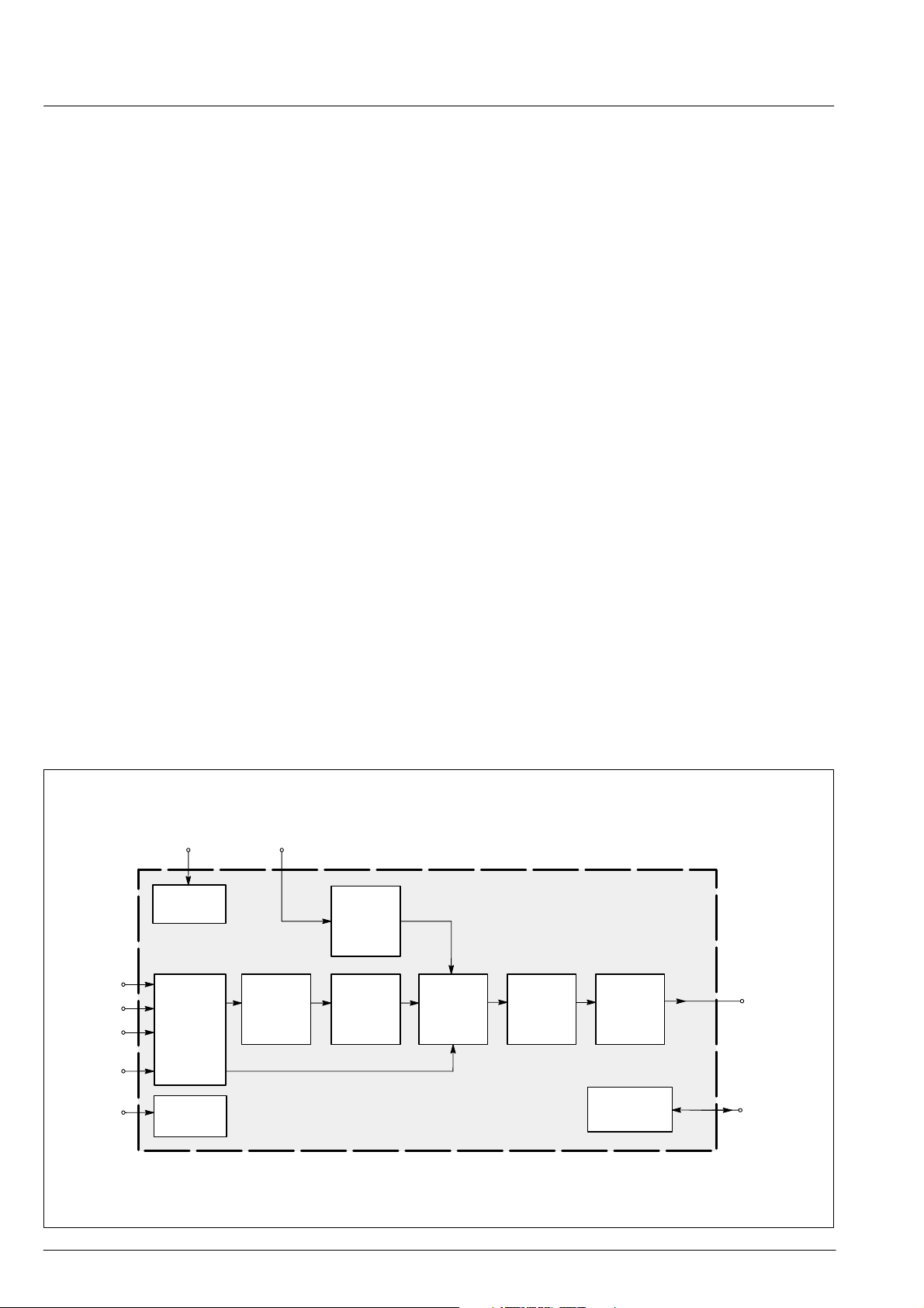
1.1. Block Diagram
The CIP 3250A contains the following main functional
blocks (see Fig.1–1):
– digital matrix RGB ⇒ YUV (Y, B–Y, R–Y)
– luma contrast and brightness correction for signals
from analog input
– color saturation and hue correction for signals from
analog input
– digital input for DIGIT 2000 or DIGIT 3000 formats
– digital interpolation to 4:4:4 format
– high quality soft mixer controlled by Fast Blank signal
– programmable delays to match digital YUVin and ana-
log RGB/YUV
– variable low pass filters for YUV output
– digital output in DIGIT 2000 and DIGIT 3000 formats,
as well as RGB 4:4:4
2
–I
C bus interface
– clock frequency 13.5...20.25 MHz
1.2. System Configurations
– analog input for RGB or YUV and Fast Blank
– triple 8 bit analog to digital converters for RGB/YUV
with internal programmable clamping
– single 6 bit analog to digital converter for Fast Blank
signal
YUV 4:1:1
YUV 4:2:2
MATRIX
(on/off)
Format
Conversion
4:4:4
CT
BR
SAT
R/V
G/Y
B/U
FSY
FSY
interface
ADC
The following figures, 1–2 and 1–3, show different basic
system applications for the CIP 3250A in the DIGIT 3000
environment. Beyond that, a stand alone application
(figure 1–4) also shows the flexibility of the CIP 3250A
in implementing simple analog video interfaces to digital
standards.
YUV 4:1:1
YUV 4:2:2
SOFT
MIXER
(4:4:4)
Adjustable
LPF
Format
Conversion
RGB 4:4:4
FBL
CLK
clock
buffer
I2C
interface
I2C
Bus
Fig. 1–1: Block diagram of the CIP 3250A Component Interface Processor
4 Micronas
Page 5
ADV ANCE INFORMATION
CIP 3250A
H,V-Sync
Clock
CVBS
Y, C
VPC32xxA
CIP3250A
100 Hz/PAL+
Feature Box
RGB/YUV
Fast Blank
Fig. 1–2: Complete DIGIT 3000 application for 100 Hz and/or PAL+
CVBS
VPC32xxA
CIP3250A
Y, C
RGB/YUV
Fast Blank
Fig. 1–3: DIGIT 3000 video front-end for ITUR-601 or square pixel data output
DDP3310B
CRT
H,V-Sync
Clock
YUV Data
CCU 3000
2
CVBS
2
I
C Bus
TV Module
RGB/YUV
Clock
CIP3250A
HSYNC, VSYNC
orthogonal
YUV pixel
Fig. 1–4: CIP 3250A in a stand alone video application for multimedia or scan rate conversion
5Micronas
Page 6
6 Micronas
CIP 3250A
R/V
G/Y
B/U
FBL
FSY
SKEW FSY AVI HSYNC VSYNC
*1)
clamp clamp clamp
AVI
*2) RGB–ADC
8
ADC 8 bit
8
ADC 8 bit
8
ADC 8 bit
6
6 bit
ADC
mode
ctrl
clamp control
12, 16
Matrix (on/off)
YUVin
CT
BR
SAT
DL1
adjust
(78)
Formatter
UV–mux
WR
RD
DL2
adjust
(48...212)
Input
LPF
4:4:4
Skew
Filter
*2) *1)
Skew
Filter
*2)
SOFT
MIX
Skew
Filter
Video
Control
Logic
AVI
Adjustable
LPF
UV–mux
Formatter
Output
72 Bit
PRIO
coder
12
16
24
AVO
R/UV
G/Y
B
3
PRIO
clock
buffer
CLK I2C Bus
Fig. 2–1: CIP 3250A block diagram
Note:
*1) Only used in DIGIT 2000 mode
*2) Only used in DIGIT 3000 mode
I2C
interface
2
CIP 3250A
ADV ANCE INFORMATION
Page 7

ADV ANCE INFORMATION
CIP 3250A
2. Functional Description
This section describes the functionality of the various
blocks shown in the block diagram of Fig. 2–1 in detail.
The CIP 3250A is controlled via an I
2
C bus interface. For
information regarding how to program the registers of
the CIP 3250A, please refer to the register list (see
Tables 2–9 and 2–10). The I
addressing to access the register. In the following, I
2
C bus interface uses sub-
2
registers are referenced by the sub-addresses given in
parenthesis; for example, I
2
C register <9>. To interface
correctly , a pin description for the CIP 3250A is given in
section 3.3.
2.1. Analog Front End
– SCART-level inputs (RGB/YUV and
Fast Blank = 1.0 Vpp, Fast Blank must be ext. clipped)
– triple 8-bit ADC for RGB/YUV
– 6 bit ADC for Fast Blank
– sampling rate 13.5 to 20.25 MHz
– no sync separation included
All analog video input signals and the analog Fast Blank
signal must be band limited to 5 MHz before analog to
digital conversion.
ue via I
2
C registers <18> and <19>. A window size of 32
or 64 sample clocks is recommended. Clamping is disabled if start and stop values are equal after reset. Once
enabled it can not be switched off. Using a coupling capacitor of 220 nF, a hum of approximately 400 mV at
50 Hz can be compensated.
2.3. Matrix
C
– matrix RGB ⇒ Y(R–Y)(B–Y):
Y = 0.299*R + 0.587*G + 0.114*B
(R–Y) = 0.701*R – 0.587*G – 0.114*B
(B–Y) = –0.299*R – 0.587*G + 0.886*B
– fixed coefficients with a resolution of 8 bits.
– matrix enable/disable for analog RGB/YUV input pro-
grammable via I2C register
The matrix of the CIP 3250A converts the digitized RGB
signals to the intermediate signals Y, R–Y, and B–Y. Enable the matrix via I
2
C register <04>MAON. The intermediate signals at the output of the matrix can be converted to YUV signals of the DIGIT 2000 system or to
YC
of the DIGIT 3000 system by the YUV control (see
rCb
section 2.4.). To omit conversion from RGB to
Y(R–Y)(B–Y), switch off the matrix and the CTBRST
block via I2C register <04>MAON and <04>CBSON.
2.4. YUV Control (on RGB-path only )
The CIP 3250A can process either analog YUV input
signals or analog RGB input signals which are ACcoupled with a nominal input voltage level of 700 mV +
3 dB (1 V
). There is no circuitry implemented for inter-
PP
nal sync separation. Input voltage range of the Fast
Blank signal is 0 to 1 V. The Fast Blank input signal is
DC-coupled.
2.2. Clamping
– internal clamping for RGB and YUV with adjustable
start and width
– black level reference only during horizontal and verti-
cal blanking interval on RGB/YUV inputs
– no proper clamping if sync is on G
In RGB mode, clamping takes place on black level (digi-
tal 16 or 8) using a clamping window as described below.
In YUV mode, clamping is done on black level (digital 16)
for Y (luma) and on saturation level zero (digital 128) for
UV (chroma) using a clamping window. Select between
RGB mode and YUV mode via I
2
C register <09>YUV.
The black level reference value (digital 16 or 8) can be
selected via I
2
C register <09>CLMPOFS. In a standard
DIGIT 2000 application without a conversion of Y (luma)
to ITUR code levels at the digital inputs (see section 2.9.
<10>YLEVEL), convert the black level to digital 32 via
2
I
C register <04>CLSEL.
– Y contrast (ct) and brightness (br) with rounding or
noise shaping and limiting to 8 bit:
Y = Y*ct + br
ct = 0...63/32 in 64 steps
br = –128...+127 in 256 steps
– UV saturation (sat) with rounding or noise shaping and
limiting to 8 bit (controllable by CCU via I
U
= (B–Y) * Usat
EXT
V
= (R–Y) * Vsat
EXT
2
C bus):
Usat,Vsat = 0...63/32 in 64 steps
(U
= [0.5*(B–Y)] * Usat
INT
V
= [0.875*(R–Y)] * Vsat)
INT
Within the CTBRST block, switched on via I
2
C register
<04>CBSON, two different options can be used to convert from (R–Y)(B–Y) to UV (PAL standard). In internal
mode (UV
), conversion to PAL standard is done be-
INT
fore the multiplication of the contents of the saturation
registers. Using the external mode (UV
EXT
) of
<04>SMODE, the user has to implement the conversion
factors via the two saturation registers (Usat, Vsat).
Since the two saturation registers can be programmed
separately , it is also very easy to convert to YC
rCb
(Stu-
dio standard) of the DIGIT 3000 system.
Contrast, brightness, and saturation can be adjusted for
the video signals of the analog input via I
2
C registers
<00> to <03>. A functional description of this circuit can
be found in figures 2–2 and 2–3 respectively.
The clamping window is programmable in reference to
the H-sync signal (see Fig. 2–13) by a start and stop val-
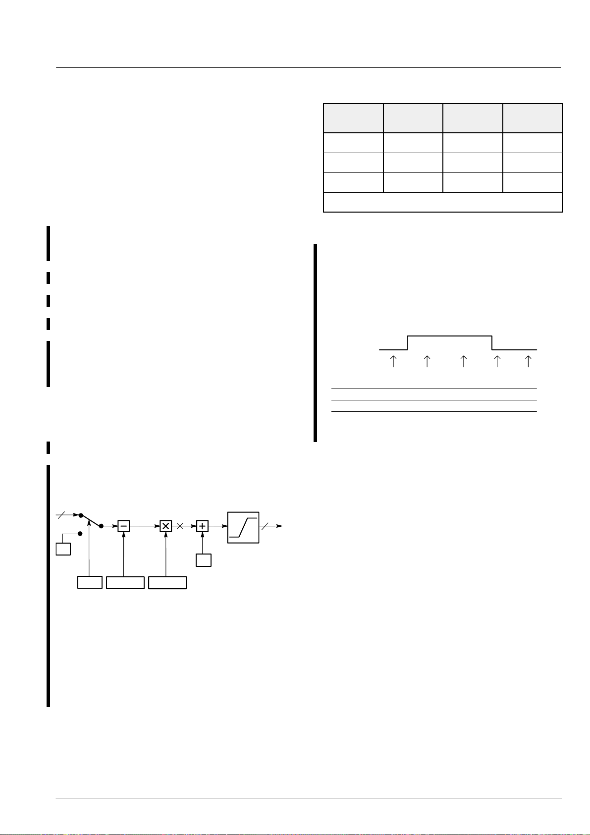
T o improve the amplitude resolution of the luma (Y) and
chroma (UV) video signals after multiplication with the
7Micronas
Page 8
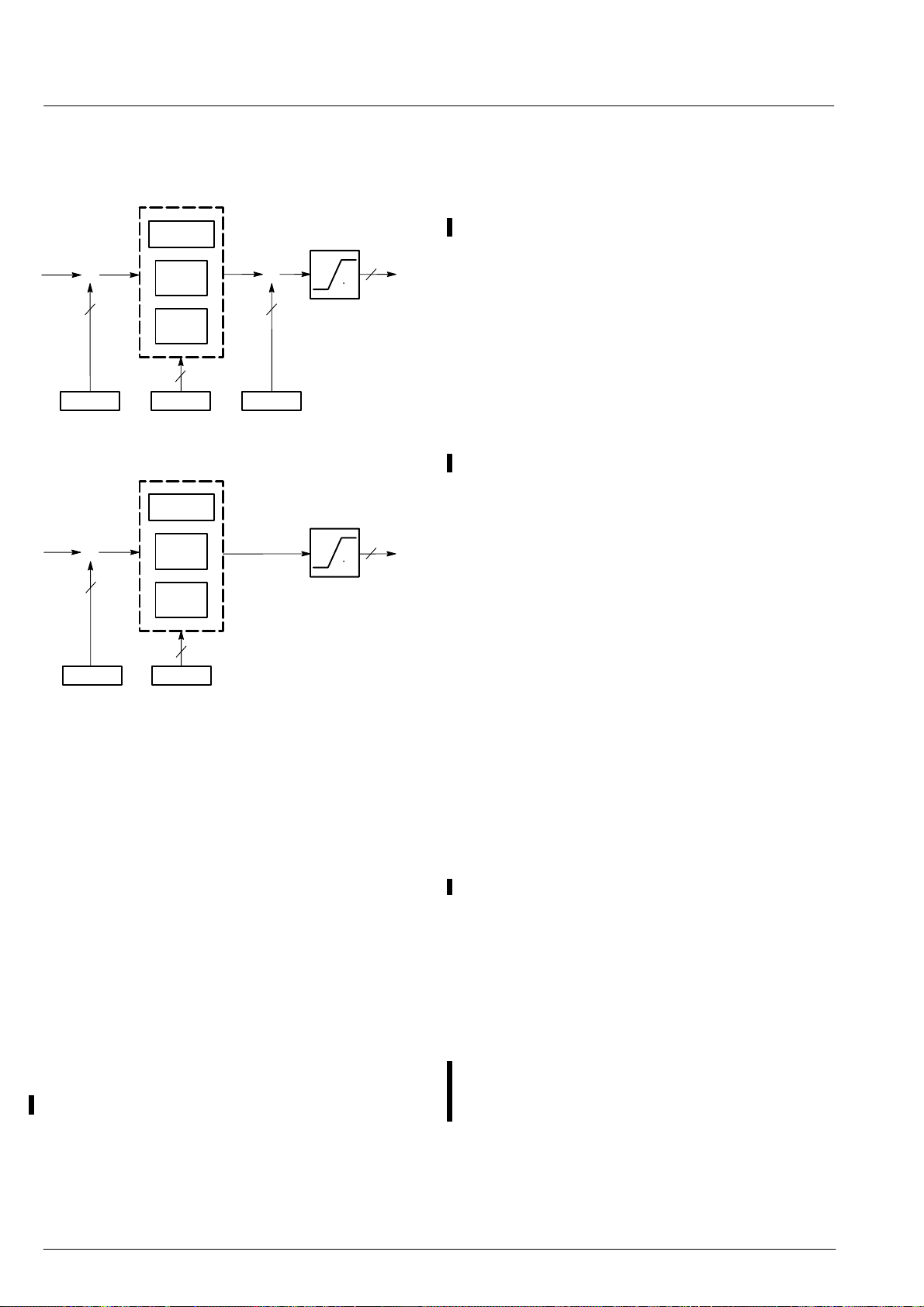
CIP 3250A
ADV ANCE INFORMATION
weighting factors (ct) and (sat), the user can select between rounding and two different modes of noise shaping (1 bit error diffusion or 2 bit error diffusion).
Rounding
Y
6 8
ct br
1 bit
Err. Diff.
2 bit
Err. Diff.
2
Select
255
I2C Registers
Y
0
8
Fig. 2–2: Luma Contrast & Brightness Adjustment
Rounding
–128
VR–Y
U
8
B–Y
sat
1 bit
Err. Diff.
6
2 bit
Err. Diff.
Select
2
I2C Registers
127
Fig. 2–3: Chroma Saturation Adjustment
2.5. Delay Adjustment
– DL1 to compensate internal processing delay of the
CIP 3250A in reference to digital YUVin
– DL1 to compensate processing delay of the DIGIT
2000 SPU chroma channel in SECAM mode
– DL2 to compensate delay between digital YUVin and
analog RGBin or FSY; as for example, produced by
ACVP or SPU.
T o mix the analog RGB/YUV input signals and the digital
YUVin input signals at the soft mixer correctly, in reference to the horizontal synchronization pulse, two processing delay adjustments can be made. In many system applications, ICs in front of the CIP 3250A cause a
fixed processing delay in the digital YUVin path. Therefore, a delay of up to 210 sample clocks can be programmed via I
2
C register <21>DL2 to match analog
RGB/YUV data with digital YUV data . If the delay is less
than 48 sample clocks, the DL1 block can be activated
(80 sample clocks) via I
2
C register <10>DL1ON to get
a value for <21>DL2 within the range of 48 to 210.
In applications where there will be no fixed delay be-
tween digital YUVin and analog RGB/YUV, the pixel
skew correction can be switched on via I
2
C register
<17>PXSKWON. In this mode, the DL2 block serves as
a variable delay to match the analog RGB/YUV data with
digital YUV data. The first pixel of analog RGB/YUV written into the DL2 block (which works like a FIFO) is selected by <21>DL2. Read of the DL2 block starts synchronously with the AVI input, which in turn marks the
first pixel in digital YUV data (see Fig. 2–14). Care must
be taken that the number of pixels stored in DL2 block
must be within the limits of 48 to 210.
In case of SECAM processing in the DIGIT 2000 environment, the digital luma and chroma signals do not
match in front of the CIP 3250A. Therefore, the I
2
C register <10>SECAM must be enabled, and fine adjustment
has to be carried out within the ACVP.
2.6. Skew Filter
Two interpolation filters perform data orthogonalization
(= skew correction) for luma and chroma in case of a
non-line-locked system clock. The skew value is serially
input via the FSY input. In a system environment where
digital YUV data are orthogonal (e.g. DIGIT 3000), the
skew correction must be set to DIGIT 3000 mode via I
2
register <04>SKWCBS in order to apply skew correction
to analog RGB/YUV data only. Additionally, the skew
correction must be switched on via I
2
C register
<04>SKWON. This has to be done in order to mix the
analog input with the digital YUV input correctly and to
output the mixed YUV signal in an orthogonal format.
For standard DIGIT 2000 operation, the skew correction
should be switched off via I
2
C register <04>SKWON, in
order to output the mixed YUV data with the same skew
values as the digital YUV input. Only in special applications (e.g. multi media), where the output connects to a
field or frame memory which processes orthogonal data,
the skew correction for mixed YUV data has to be
switched on and set to DIGIT 2000 mode via I
2
C register
<04>SKWCBS.
2.7. Fast Blank Processing
– mixing of RGB-path and YUV-path in YUV 4:4:4 format
controlled by the Fast Blank signal
– linear or nonlinear mixing technique selectable
– programmable polarity of Fast Blank signal
– programmable step response of Fast Blank signal
– RGB-path or YUV-path can be statically selected
– Fast Blank signal monitoring
2.7.1. Soft Mixer
In the Fast Blank signal path, special hardware is supplied to improve edge effects, such as blurring because
of band limiting in the analog front end. Different step responses are user selectable via I
2
C register <12>MIX-
AMP, still obtaining high quality phase resolution. Also,
C
8 Micronas
Page 9
ADV ANCE INFORMATION
CIP 3250A
the polarity of the Fast Blank signal can be changed via
2
I
C register <12>MIXAMP. The I2C register
<11>FBLOFF influences the phase delay between the
RGB path and the Fast Blank signal (see Fig. 2–4).
Additionally, a delay of –1 to 2 clocks between the Fast
Blank signal and the RGB-path is programmable via I
2
register <16>FBLDEL. By selecting a positive delay,
shadowing of characters can be obtained, if the background color of the RGB-path is set to black.
With the built-in linear mixer, the CIP 3250A is able to
support simple AB roll techniques between analog input
(A) and digital YUV input (B):
VideoOut = A * (1 – FBLMIX/32) + B * FBLMIX/32,
controllable via the Fast Blank signal (FBL):
FBLMIX = INT[(FBL – FBLOFF)* MIXAMP/2] + 16,
with FBL of values from 0 to 63. The mixing coefficient
FBLMIX resolves 32 steps within the range from 0 to 32
(dependent on step response chosen via I2C register
<12>MIXAMP) (see Fig. 2–4).
When the I2C register bit <16>FBLCLP is enabled, the
soft mixer operates independently of the analog Fast
Blank input. FBL is clamped to digital 31 (see Fig. 2–4).
Mixing between RGB-path and YUV-path is controllable
via the I
2
C register <11>FBLOFF .
Table 2–1: Source selection of soft mixer
<11>
PASSRGB
0 X X RGB
C
1 0 MIX YUV/RGB
1 1 X YUV
X: don’t care
<06>
PASSYUV
Fast Blank
signal
Source
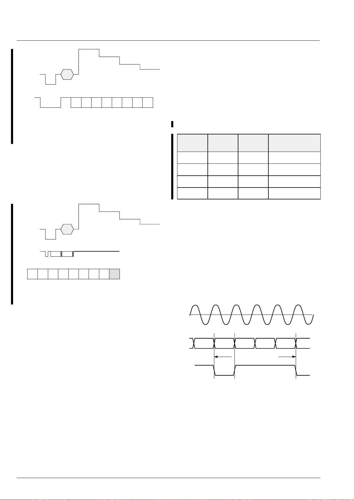
2.7.2. Fast Blank Monitor
Bits 0 to 3 of I2C register <27> are monitoring the analog
Fast Blank input. Reading I2C register <27> Fig. 2–5 displays the contents depending on the analog FBL input
signal.
analog fast
blank input
<27>FBLSTAT
<27>FBLRISE
<27>FBLFALL
<27>FBLHIGH
2
C
reading I
register <27>
0 1100
01 00
00 01
01 110
0
0
Fig. 2–5: Fast Blank Monitor
2.8. FSY Front Sync and AVI Active Video In
FBL (0...63)
FBLMIX
32
0
I2C Registers
6
31
0
6
1
fblclp
fbloff mixamp
1/2
16
Fig. 2–4: Fast Blank Processing
Select the linear mixer or the nonlinear mixer via I2C register <12>SELLIN. If the nonlinear mixer is selected, a
dynamic delay control of the analog RGB/YUV input can
be chosen, to avoid edge artefacts of the RGB/YUV signal (e.g. shading), during transition time of Fast Blank
signal with the I2C register <12>CTRLDLY.
In some applications, it is desired to disable the control
by the Fast Blank signal and to pass through the digital
YUVin path or the analog RGB/YUV path. This is possible by adequately programming the I
2
C registers
<06>PASSYUV and <11>PASSRGB (Table 2–1).
– DIGIT 2000 chroma sync detection
– DIGIT 2000 throughput of 72-bit data and clock
– skew data input for DIGIT 2000
– skew data input for DIGIT 3000
– HSYNC as timing reference for clamping pulse gener-
ator
– active video input to indicate valid video data and to
synchronize chroma multiplex for DIGIT 3000
The FSY input and the AVI input are used to supply all
synchronization information necessary. Three basic
modes of operation can be selected via I
2
C registers
<06>D2KIN, <17>D2KSYNC, <17>SYNCSIM, and
<17>P72BEN.
In a DIGIT 2000 system environment, the CIP 3250A receives the synchronization information at the FSY input
via the DIGIT 2000 SKEW-protocol. The A VI Input may
be connected to ground GND or VDD (see section
2.14.).
9Micronas
Page 10
CIP 3250A
input
analog
video
Skew
data
Bit:
(not in scale)
skew
MSB
01234567
skew
LSB
ig–
ig–
nored
nored
V: Vert. sync
0 = off
1 = on
V
ADV ANCE INFORMATION
DIGIT 2000, and the YUV 4:2:2 (16 bit) standard from
DIGIT 3000. Therefore, the CIP 3250A can be used in
either the DIGIT 2000 system environment or the DIGIT
3000 system environment. Refer to I
2
C registers
<06>DELA YU, <10>UVFRM3, and <10>UVFRM1 for a
correct setup. Additionally, within the DIGIT 2000 system, a Y (luma) format conversion to ITU-R 601 can be
achieved via programming the I
2
C register <10>YLE-
VEL.
Table 2–2: Digital input selection
Fig. 2–6: DIGIT 2000 skew data
In a DIGIT 3000 system environment, the CIP 3250A receives the synchronization information at the FSY input
via the DIGIT 3000 FSY -protocol (see Fig. 2–7). The A VI
input receives the chroma multiplex information implicitly with the rising edge of the AVI signal.
input
analog
video
FSY
skew
F1
MSB
F0, F2...F5: reserved
F0
F1
skew
ig–
LSB
nored
(not in scale)
ig–
V
nored
Parity
V: Vert. sync
0 = off
1 = on
Fig. 2–7: DIGIT 3000 front sync format
<06>
DELAYU
<11>
UVFRM3
<11>
UVFRM1
Digital
Input Format
0 0 0 DIGIT 2000 4:2:2
0 0 1 DIGIT 2000 4:1:1
1 1 0 DIGIT 3000 4:2:2
1 0 0 MAC
2.9.1. The Chroma Demultiplexers
In DIGIT 2000 mode, via pins 36 to 39, the CIP 3250A
receives the V and U signals from the C0 to C3 outputs
of the color decoder, time-multiplexed in 4-bit nibbles
(Fig. 2–8). For the digital signal processing, the 4-bit V
and U chroma nibbles are demultiplexed to 8-bit signals
by the V and U demultiplexers. Both demultiplexers are
clocked by the main clock. They are synchronized to the
V and U transmission during the vertical blanking period.
In a stand alone application, for example, RGB-analogto-digital conversion, a horizontal sync pulse must serve
the FSY input, and a vertical sync pulse must serve the
AVI input. The polarity of these two sync pulses can be
programmed via I
2
C registers <10>AVIINV and
<07>FSYINV.
Inside the CIP 3250A, synchronization information is be-
ing decoded and used to control clamping, DL2, skew filters, video control logic, input formatter, and output formatter as shown in Fig. 2–1.
2.9. Digital Input Formats
– YUV 4:2:2 (16 bit) from DIGIT 2000 and DIGIT 3000
(YUV as well as YCrCb)
– YUV 4:1:1 (12 bit) from DIGIT 2000
– input levels according to DIGIT 2000/DIGIT 3000
The CIP 3250A supports the YUV 4:1:1 (12 bit) standard
from DIGIT 2000, the YUV 4:2:2 (16 bit) standard from
a)
H
b)
U MSB V LSB V MSB U LSB U MSB
L
four clock periods
H
c)
L
Fig. 2–8: Timing diagram of the multiplexed color difference signal transfer between decoder and CIP
3250A
Notes to Fig. 2–8:
a) CLK main clock signal
b) Multiplexed color difference signals from PVPU/
ACVP/SPU/VSP/DMA to DTI 2260
c) Sync pulse on C0 output during sync time in vertical
blanking interval.
10 Micronas
Page 11

ADV ANCE INFORMATION
CIP 3250A
2.10. YUVin Interpolator (LPF 4:4:4)
– UV-Interpolation 4:1:1 or 4:2:2 ⇒ 4:4:4
In order to mix the digital input data with the 4:4:4 video
standard from the analog RGB/YUV input, correctly, the
chroma samples of the digital input have to be interpolated.
In case of YUV 4:1:1 input from DIGIT 2000, a two stage
interpolation filter is implemented. In the first stage, an
interpolation filter is used, which converts the YUV 4:1:1
standard into the YUV 4:2:2 standard.
In the second stage, the interpolation is from the YUV
4:2:2 to YUV 4:4:4.
In the case of YUV 4:2:2 input, only the second stage is
necessary.
Refer to I
and <10>UVFRM1 to choose the correct interpolation
filters (see Fig. 2–2).
2
C registers <06>DELAYU, <10>UVFRM3,
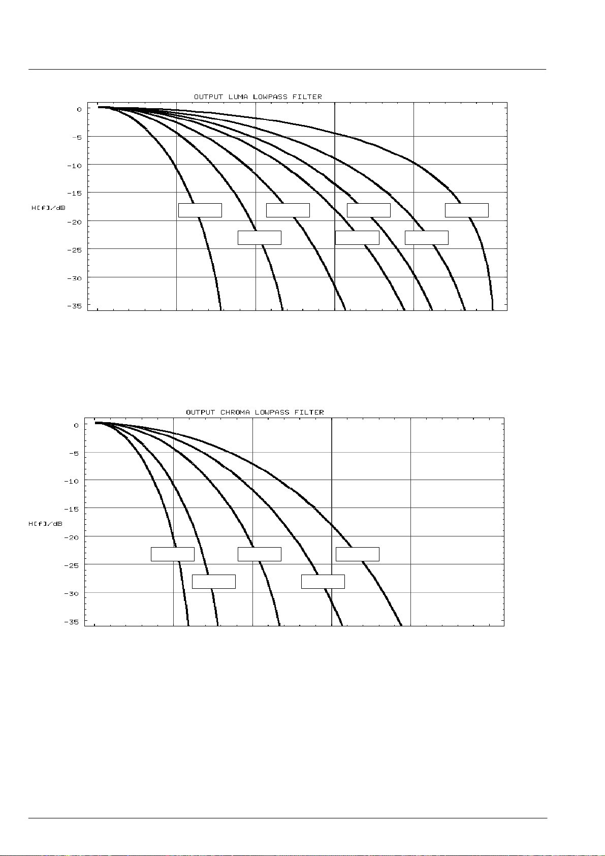
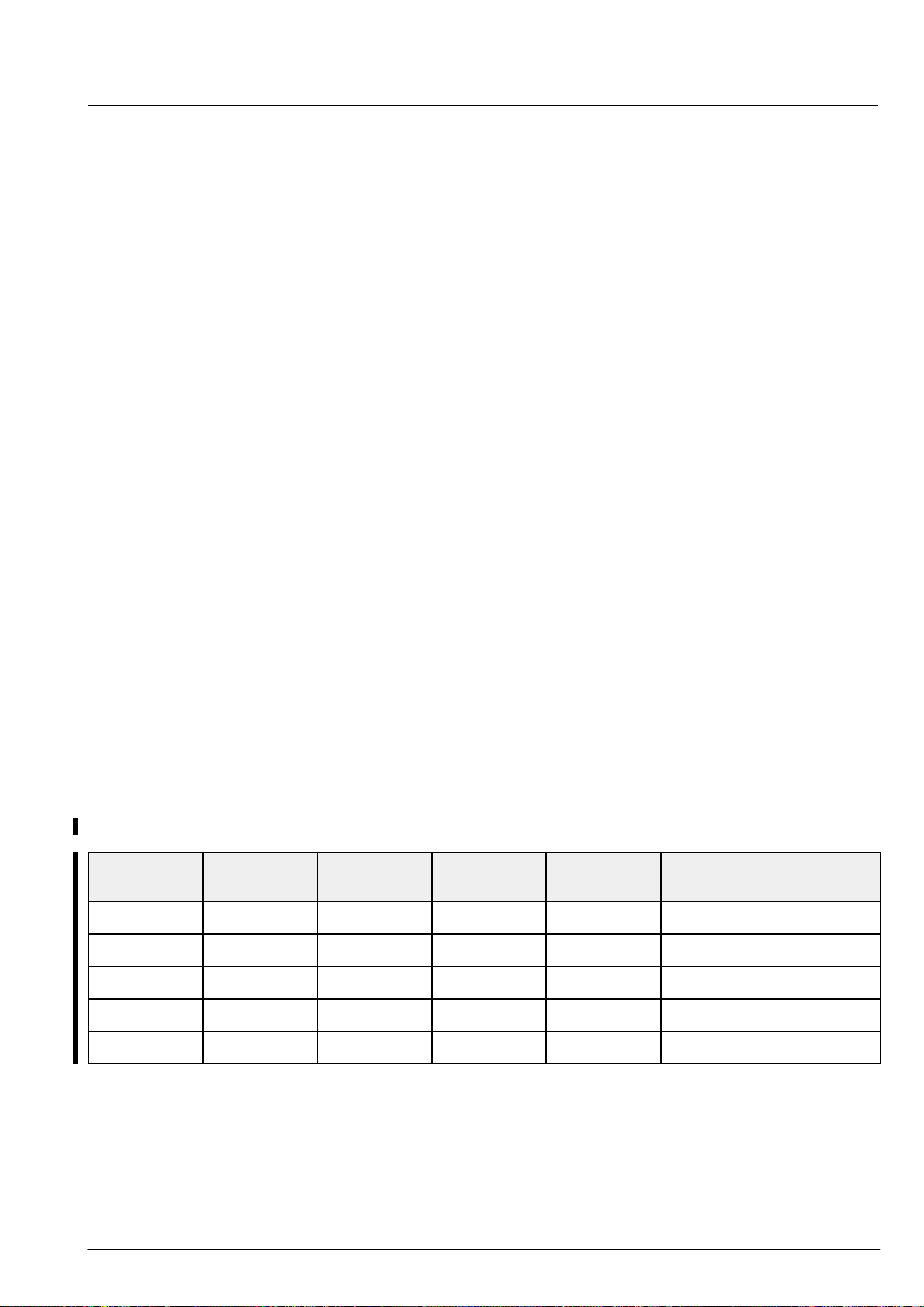
2.11. YUV Output Low-pass Filter 4:2:2 and 4:1:1
– Y low-pass filter with 7 selectable cutoff frequencies
– UV low-pass decimation filter 4:4:4 ⇒ 4:2:2/4:1:1 with
5 selectable cutoff frequencies
To meet the bandwidth requirements of different video
standards, such as 4:2:2 or 4:1:1 at various sampling
frequencies, the luma signal (Y) and the chroma signal
(UV) can be lowpass filtered. There are 7 different cutoff
frequencies selectable for luma, via I
<05>LPFLUM and 5 different cutoff frequencies selectable for chroma, via I
spectra of the luminance filters are shown in Fig. 2–9,
and the spectra of the chrominance filters are shown in
Fig. 2–10.
2
C register <07>LPFCHR. The
2
C register
11Micronas
Page 12
CIP 3250A
0 0.1*fs 0.2*fs 0.3*fs 0.4*fs 0.5*fs
ADV ANCE INFORMATION
Y7 Y5 Y3 Y1
Y6 Y4 Y2
Fig. 2–9: Spectra of selectable luminance filters
UV5
UV4 UV2
0 0.1*fs 0.2*fs 0.3*fs 0.4*fs 0.5*fs
UV3 UV1
Fig. 2–10: Spectra of selectable chrominance filters
12 Micronas
Page 13
ADV ANCE INFORMATION
CIP 3250A
2.12. Selectable RGB/YUV Output Formats
– RGB, 8-bit pure binary (24 bit)
– YUV 4:2:2 (16 bit) for DIGIT 2000, DIGIT 3000, and
Philips/Siemens
– YUV 4:1:1 (12 bit) for DIGIT 2000 and Philips/Siemens
– UV format selectable between 2’s complement and
binary offset
In a first stand alone application, the CIP 3250A can
serve as a RGB video analog-to-digital converter to output digital R, G, and B in a pure binary format, 8 bits pure
binary per channel, and a sampling rate between 13.5
MHz and 20.25 MHz.
In a second stand alone application, the CIP 3250A can
serve as a YUV or RGB (with the matrix switched on) video analog-to-digital converter to output digital YUV , supporting various formats such as YUV 4:1:1 (12 bit) from
DIGIT 2000 and Philips, YUV 4:2:2 (16 bit) from DIGIT
2000 and DIGIT 3000, or YUV 4:2:2 (16 bit) industry
standard. Additionally, the signed format of the UV signal is programmable between 2’s complement and
binary offset. A sampling rate between 13.5 MHz and
20.25 MHz can be selected, and the YUV output data
can be low pass filtered.
In a DIGIT 2000 environment, the CIP 3250A can process either RGB or YUV signals from the analog Input,
mix it with the digital YUV Input data – controlled by the
Fast Blank input, and generate low pass filtered output
data in the YUV 4:1:1 (12 bit) DIGIT 2000 format. A sampling rate locked to the color subcarrier frequency (4*fsc)
for the NTSC or PAL video standard has to be used.
In a DIGIT 3000 environment, the CIP 3250A can process either RGB or YUV signals from the analog input,
mix it with the digital YUV input data – controlled by the
Fast Blank input, and generate low pass filtered output
data in the YUV 4:2:2 (16 bit) DIGIT 3000 format. Additionally, the signed format of the UV signal is programmable between 2’s complement and binary offset. The
sampling rate is derived from the VPC 320x and ranges
from 13.5 to 20.25 MHz for all of the video standards.
The U and V chrominance samples are transmitted in
multiplex operation. Depending on the application, the
CIP 3250A provides the following different output formats of the YUV signals (selectable via I
– 4:1:1 orthogonal output format for DIGIT 3000 applica-
tions
– 4:2:2 orthogonal output format for DIGIT 3000 applica-
tions
– 4:1:1 output format for standard DIGIT 2000 applica-
tions
– 4:2:2 output format for DIGIT 2000 applications
Refer to I
output format. Additionally , the CIP 3250A provides conversion of ITURY (luma) to DIGIT 2000 Y (luma) output
black levels, selectable via I
A programmable two-dimensional active video signal
(A VO) allows the write control of external video memory
directly. The characteristic of the YUV output is selectable between open-drain or push-pull.
2
C registers <15> to <16> to select the desired
2
C register <16>ADD16Q.
2
C-Bus):
Table 2–3: Digital output selection
<15>
YUVO
1 1 0 0 0 DIGIT 2000 4:1:1
1 1 1 0 0 orthogonal 4:1:1
1 0 0 1 1 DIGIT 2000 4:2:2
1 0 1 0 0 DIGIT 3000 4:2:2
0 0 0 0 0 4:4:4
<15>
MOD411ON
<15>
IND
<15>
UVSW
<15>
DTI
Digital
Output Format
13Micronas
Page 14
CIP 3250A
ADV ANCE INFORMATION
2.12.1. DIGIT 2000 4:1:1 Output Format
The DIGIT 2000 4:1:1 output format is shown in Tables
2–4 and 2–5. A control signal for the chroma multiplex
is transmitted during the vertical blanking interval (see
Section 2.9.1.).
Table 2–4: Bit map of DIGIT 2000 4:1:1 format
Luma
Y
1
Y
2
Y
3
Y
4
Chroma
C
, C
3
C
, C
2
C1 , C
C
, C
0
Note: U
3
7
6
5
4
Y
x
V
2
2
V
2
1
V
2
0
V
2
x = pixel number and y = bit number
7
V
2
6
V
2
5
V
2
4
V
2
3
U
1
2
U
1
1
U
1
0
U
1
7
U
1
6
U
1
5
U
1
4
U
1
Table 2–5: Sampling raster of DIGIT 2000 4:1:1 format
Luma
Y
1
Y
2
Y
3
Y
4
Y
5
Chroma
Table 2–6: DIGIT 2000 4:2:2 output format
Luma
Y
1
Y
2
Y
3
Y
4
Chroma
C
7
C
6
C
5
C
4
C
3
C
2
C
1
C
0
Note: U
7
V
2
6
V
2
5
V
2
4
V
2
3
V
2
2
V
2
1
V
2
0
V
2
Y
x = pixel number and y = bit number
x
7
U
1
6
U
1
5
U
1
4
U
1
3
U
1
2
U
1
1
U
1
0
U
1
7
V
4
6
V
4
5
V
4
4
V
4
3
V
4
2
V
4
1
V
4
0
V
4
7
U
3
6
U
3
5
U
3
4
U
3
3
U
3
2
U
3
1
U
3
0
U
3
2.12.3. DIGIT 3000 Orthogonal 4:2:2 Output Format
The DIGIT 3000 orthogonal 4:2:2 output format is compatible to the industry standard. The U and V samples
are skew corrected and interpolated to an orthogonal
sampling raster, e.g. every line starts with the current U
pixel (see Table 2–7).
line 1
line 2
line 3
line 4
line 5
V
2L
U
XM
U
XL
V
1M
V
2L
V
2M
V
3L
U
XM
U
XL
V
2M
U
1L
V
3M
V
4L
U
XM
U
1L
U
1M
U
2L
V
4M
V
5L
U
1M
V
6L
U
2M
U
3L
V
5M
V
6L
Note: Uxy x = pixel number and y = LSB/MSB nibble
pixel no. X indicates an invalid sample at the
beginning of the line
2.12.2. DIGIT 2000 4:2:2 Output Format
In the DIGIT 2000 4:2:2 output format, the U and V samples are non-orthogonal (calculated from adjacent pixel,
e.g. line n starts with a V pixel and line (n+1) starts with
a U pixel (see Table 2–6).
Table 2–7: Orthogonal 4:2:2 output format
Luma
Y
1
Y
2
Y
3
Chroma
C
7
C
6
C
5
C
4
C
3
C
2
C
1
C
0
Note: U
7
U
1
6
U
1
5
U
1
4
U
1
3
U
1
2
U
1
1
U
1
0
U
1
Y
x = pixel number and y = bit number
x
7
V
1
6
V
1
5
V
1
4
V
1
3
V
1
2
V
1
1
V
1
0
V
1
7
U
3
6
U
3
5
U
3
4
U
3
3
U
3
2
U
3
1
U
3
0
U
3
Y
4
7
V
3
6
V
3
5
V
3
4
V
3
3
V
3
2
V
3
1
V
3
0
V
3
14 Micronas
Page 15

ADV ANCE INFORMATION
2.12.4. Orthogonal 4:1:1 Output Format
The orthogonal 4:1:1 output format is compatible to the
industry standard. The U and V samples are skew corrected and interpolated to an orthogonal sampling raster
(see Table 2–8).
Table 2–8: 4:1:1 orthogonal output format
CIP 3250A
<23>AVHSTRT <24>AVHLEN
AVO
<26>AVVSTOP<25>AVVSTRTstart of field
Fig. 2–11: Programmable AVO signal
Luma
Y
1
Y
2
Y
3
Y
4
Chroma
C
, C7
3
C
, C6
2
C
, C5
1
C
, C
0
Note: U
7
U
1
6
U
1
7
V
1
6
4
Y
x
V
1
x = pixel number and y = bit number
5
U
1
4
U
1
5
V
1
4
V
1
3
U
1
2
U
1
3
V
1
2
V
1
1
U
1
0
U
1
1
V
1
0
V
1
2.12.5. YUV Output Levels
The Y output black level of the CIP 3250A can be converted from ITU-R 601 Standard (digital 16) to DIGIT
2000 Standard (digital 32) via I
2
C register
<16>ADD16Q.
2.13. I/O Code Levels
– ITU-R/DIGIT 3000 code levels:
Y or RGB = 16...240, clamp level = 16
UV = ±112, bias level = 0
Select the desired mode via I2C register <17>AVINT. If
the AVO signal is derived from the AVI signal, the I
2
registers <22>A VDL Y can be used to compensate internal processing delays of the CIP 3250A.
2
I
C register <22>A VPR can be used to precede the AVO
signal in relation to the RGB/YUV data output up to 3
clocks.
2.15. PRIO Interface
– real-time bus arbitration for 8 sources in DIGIT 3000
picture bus.
Up to eight digital YUV or RGB sources (main decoder,
PIP, OSD, Text, etc.) may be selected in real-time by
means of a 3 bit priority bus. Thus, a pixelwise bus arbitration and source switching is possible. It is essential
that all YUV-sources are synchronous and orthogonal.
In general, each source (= master) has its own YUV bus
request. This bus request may either be software or
hardware controlled, i.e. a fast blank signal. Data collision is avoided by a bus arbiter that provides the individual bus acknowledge, in accordance to a user defined
priority.
C
– or DIGIT 2000 code levels:
Y = 32...127, clamp level = 32
UV = ±127, bias level = 0
2.14. AVO Active Video Output
In a DIGIT 3000 system environment, the A VO signal is
equivalent to the delayed AVI signal. It signalizes valid
video data and chroma multiplex at the output of the
CIP 3250A. Furthermore, the AVO signal can be used to
control the write enable of a frame memory . The polarity
of the AVO signal is programmable via I
2
C register
<10>AVOINV.
In a DIGIT 2000 system environment, the AVO signal
can be programmed via I
2
C registers <23> to <26> to
define a window of valid video data at the output of the
CIP 3250A (see Fig. 2–11).
Each master sends a bus request with its individual
priority ID onto the PRIO-bus and immediately reads
back the bus status. Only in case of positive arbitration
(send-PRIO-ID = read-PRIO-ID), the RGB/YUV outputs
become active and the data is send. PRIO requests
must be enabled by I
2
C register <14>PRIOEN.
The requests asserted by the CIP 3250A may be generated by two different sources, which are selectable by
2
I
C register <09>PRIOSRC. With the first source, the
CIP 3250A asserts requests only when the AVO signal
is active, else RGB/YUV outputs are tristated. With the
second source, the CIP 3250A asserts continuous requests where the YUV data are forced to “clamp/bias
level data” (see section 2.13.) during the time that the
AVO signal is inactive.
If only one source is connected to the YUV bus, the outputs GL, RC, and B may drive the bus during a full clock
cycle. This can be selected by I
2
C register <06>HALFOUT. If more than one source is connected to the YUV
bus, the output drivers must be switched to driving only
during the first half of clock cycle to avoid bus collision.
In the last case, the layout of the PCB must consider that
15Micronas
Page 16

CIP 3250A
data on YUV bus must be kept dynamically for a half
clock cycle. Thus, capactitvie coupling from other signals to YUV bus must be avoided or reduced to a tolerable minimum.
This procedure has many features which have an impact
on the appearance of a TV picture:
– real-time bus arbitration (PIP, OSD, ...)
– priorities are software configurable
– different coefficients for different sources
ADV ANCE INFORMATION
2.16. I
2
C Serial Bus Control
Communication between the CIP 3250A and the external controller is done via I
2
I
C bus slave interface and uses I2C clock synchronization to slow down the interface if required. The I
interface uses one level of subaddressing: one I
2
C bus. The CIP 3250A has an
2
C bus
2
C bus
address is used to address the IC and a subaddress selects one of the internal registers.
The registers of the CIP 3250A have 8 bit data size. All
registers are writeable (except subaddress hex27) and
readable as well. Register bits of parameter addresses,
which are marked with an X in the description field of the
register table, must be set to zero. All registers are initialized to zero with reset.
Figure 2–12 shows I
2
C bus protocols for read and write
operations of the interface.
S
1101110
S
1101110 1101110
SDA
SCL
WP1 byte Data
Ack
W
Ack
0111 1100
0111 1100 RS Ack
SP
Ack
Ack
1
0
Ack
I2C write access
P1 byte Data
Nak
W= 0
R=1
Ack = 0
Nak = 1
S = Start
P = Stop
Device Address = 110 1110[R/W]
2
C read access
I
Fig. 2–12: I2C Bus Protocol
16 Micronas
Page 17

ADV ANCE INFORMATION
CIP 3250A
Table 2–9: The I2C-bus addresses of the CIP 3250A – Device Address: 6E Hex (7 bit, R/W bit omitted, see Sec. 2.16.)
Bit
Sub.
Addr.
No.
00
01
02
03
04
05
06
07
08
09
10
11
12
13
14
15
16
17
MSB
LSB
76543210
NOISSU
noise shaping of U
NOISSV
noise shaping of V
NOISSY
noise shaping of Y
CBSON
CTBRST block
enable
1
PASSYUV
soft mixer control
0
FSYINV
polarity FSY
TESTLUY
test y channel
TESTCLP
test clamping
0
AVOINV
polarity AVO
–
FBLTEN
Fast Blank test
0
PRIOEN
access to Picture Bus
1
UVSW
UV multiplex of
YUV output
–
FBLCLP
static Fast Blank
0
SYNCIN
UV sync control
of YUVin
–
–
–
–
SMODE
saturation mode
0
D2KIN
input amplifier of
digital YUVin
–
0
YUV
analog input select
0
AVIINV
polarity AVI
–
PASSRGB
soft mixer control
1
amplification of Fast Blank amplitude
UV output format
delay Fast Blank vs. analog RGB/YUV
SYNCOUT
UV sync control
of YUV output
MIXAMP
DTI
–
FBLDEL
–
CLSEL
clamping offset for Y
DELAYU
UV format of YUVin
SE_4_8Q
analog gain control
SECAM
delay for SECAM
1
PRIOID
set PRIO priority
IND
UV output format
0
NEGCLK
select active
clockedge
0
–
0
–
–
–
–
TESTCHU
test u channel
0
delay of YUVin
BRY
brightness correction of Y
0
MAON
matrix block
enable
1
LPFLUM
luma low pass filter selection
HALFOUT
output drive
duration
0
SELAMP
analog gain control
DL1ON
––––
override value for PRIO-interface
BINO
UV sign of
output format
–
adjust Y output delay
AVINT
AVO control
–
SKWON
skew correction
–
CYLUM1
Y low pass filter
offset correction 1
LPFCHR
chroma low pass filter selection
0
UVBINCON
UV sign of YUVin
adjust delay of RGB/YUV-path
OVR
–
PUDIS
disable pull up
of YUV/RBG output
YUVO
select RGB/YUV
output format
YDEL
–
PXSKWON
pixel skew corretion
SATU
saturation multiplier of U
32
SATV
saturation multiplier of V
32
SATY
contrast multiplier of Y
32
SKWCBS
enable
–
–
––
Fast Blank offset correction
skew filter mode
Y low pass filter
offset correction 2
TESTCHV
test v channel
0
RGB clamping offset
UV format of YUVin
FBLOFF
31
CYLUM2
CLMPOFS
UVFRM3
SELDLY
1
–
MOD411ON
UV output format
–
ADD16Q
black level
of Y output
P72BEN
72 bit data bypass
–
–
–
0
Picture Bus and PRIO bus
–
–
–
ATST
testbits
0
CYCHR1
UV low pass filter
offset correction 1
–
TESTFBL
test fbl channel
0
AVODIS
disable ACVOUT
–
UVFRM1
UV format of YUVin
SELLIN
select soft mixer
0
LOAD
adjust load strength of
–
select UV output sample from 4:4:4
DL422Y
additional
Y output delay
–
D2KSYNC
sync input at
FSY-pin
–
UV low pass filter
offset correction 2
and IDDQ test
PRIOSRC
PRIO request
convert Y format
CDEL
–
UV output delay
H-sync, V-sync
CYCHR2
ICLPTST
test fbl clamp
Source for
YLEVEL
CTRLDLY
delay control
DL422C
additional
SYNCSIM
input
–
0
1
–
0
–
–
17Micronas
Page 18

CIP 3250A
Table 2–9: The I2C-bus addresses of the CIP 3250A, continued
Bit
Sub.
Addr.
No.
18
19
20
21
22
23
24
25
26
27
MSB
76543210
CLPSTRT
start of clamping window
–
CLPSTOP
stop of clamping window
–
SKEWLAT
latch time for sub-pixel skew value
–
DL2
–
delay AVI to AVO to compensate CIP 3250 A processing delay
AVHSTRT
horizontal start of AVO
–
AVHLEN
horizontal length of AVO
–
AVVSTRT
vertical start of AVO
–
AVVSTOP
vertical stop of AVO
–
delay between YUV output and AVO
AVPR
–
fifo delay adjust for RGB/YUV-path
– ––––
FBLSTAT
static FBL read
ADV ANCE INFORMATION
AVDLY
–
FBLRISE
dynamic FBL read
rising edge falling edge high level
FBLFALL
dynamic FBL read
LSB
FBLHIGH
dynamic FBL read
18 Micronas
Page 19

ADV ANCE INFORMATION
CIP 3250A
Table 2–10: I2C-Bus operation – Device Address: 6E Hex (7 bit, R/W bit omitted, see Sec. 2.16.)
SubAddress
(decimal)
Label Bit No.
(LSB = 0)
Typical
Operation
Value
Function
I2C registers for ADC and CLAMPING
09 YUV 6 0 analog input select
18 CLPSTRT 7–0 30 start of clamping window
19
09 CLMPOFS 2 0 RGB clamping offset
04 CLSEL 5 0 Y (luma) black level adjust at RGB-path
09 SELAMP 4–3 0 analog gain control
09 SE_4_8Q 5 0 analog gain control
CLPSTOP 7–0 50 stop of clamping window
0 = RGB
1 = YUV
(0...255)*2 clocks after H-sync (see Fig. 2–13)
(0...255)*2 clocks after H-sync (see Fig. 2–13)
[note: – maximum window size: 64 sample clocks]
[ – minimum window size: 6 sample clocks]
0 = +16 (digital)
1 = +8 (digital)
0 =convert Y (luma) black level from digital 16 to 32 (DIGIT 2000)
1 =Y (luma) black level at digital 16 (ITU-R 601 Standard)
0 = 1/8
1 = 1/16
2 = 1/32
0 = 1/8
1 = 1/4
I2C registers for MATRIX
04 MAON 4 1 matrix block
0 = matrix off (YUV input or RGB bypass)
1 = matrix on (RGB to Y(R–Y)(B–Y))
I2C registers for CONTRAST / BRIGHTNESS / SATURATION
04 CBSON 7 1 CTBRST block
03 BRY 7–0 0 brightness correction of Y (luma) in CTBRST block
02 SATY 5–0 32 contrast multiplier of Y (luma) in CTBRST block
02 NOISSY 7,6 0 noise shaping of Y (luma) in CTBRST block
00 SATU 5–0 32 saturation multiplier of U (chroma) in CTBRST block
00 NOISSU 7,6 0 noise shaping of U (chroma) in CTBRST block
01 SATV 5–0 32 saturation multiplier of V (chroma) in CTBRST block
01 NOISSV 7,6 0 noise shaping of V (chroma) in CTBRST block
04 SMODE 6 0 saturation mode of UV (chroma) in CTBRST block
0 = bypassed ( for dig. RGB bypass only (<04>MAON=0))
1 = on
Y + (–128...127)
Y * (0...63)/32
0 = off (rounding is activated)
2 = 1 bit error diffusion
3 = 2 bit error diffusion
U * (0...63)/32
0 = off (rounding is activated)
2 = 1 bit error diffusion
3 = 2 bit error diffusion
V * (0...63)/32
0 = off (rounding is activated)
2 = 1 bit error diffusion
3 = 2 bit error diffusion
0 = internal PAL (U * 0.5, V * 0.875)
1 = external (U * 1, V * 1)
19Micronas
Page 20

CIP 3250A
Table 2–10: I2C-Bus operation, continued
ADV ANCE INFORMATION
SubAddress
(decimal)
Label Bit No.
(LSB = 0)
Typical
Operation
Value
Function
I2C registers for OUTPUT FORMATTER
15 YUVO 3 1 select video component output format
16 ADD16Q 2 1 black level of Y (luma) output
15 MOD411ON 2 0 UV (chroma) output format
15 BINO 4 0 UV (chroma) sign of output format
15 CDEL 1–0 0 select UV (chroma) output sample from 4:4:4 format
15 IND 5 1 UV (chroma) output format
15 UVSW 7 0 UV (chroma) multiplex of output format
15 DTI 6 0 UV (chroma) output format
16 YDEL 4–3 0 adjust Y (luma) output delay in reference to UV (chroma) output
16 DL422Y 1 0 additional Y (luma) output delay
16 DL422C 0 0 additional UV (chroma) output delay
0 = output formater off (i.e. RGB or YUV output with format 4:4:4)
1 = output formater on (i.e. YUV output with format 4:2:2 or 4:1:1)
0 = Convert Y black level at output from ITU-R 601 Standard
to DIGIT 2000 Standard (digital 32)
1 = Y black level at output unchanged
0 = 4:2:2
1 = 4:1:1
0 = two’s complement
1 = binary offset
(0...3)
0 = DIGIT 2000
1 = DIGIT 3000 / orthogonal
0 = DIGIT 3000 4:2:2 / DIGIT 2000 4:1:1 / orthogonal 4:1:1
1 = DIGIT 2000 4:2:2
0 = DIGIT 3000 4:2:2 / DIGIT 2000 4:1:1 / orthogonal 4:1:1
1 = DIGIT 2000 4:2:2
(0...3) clocks
(0...1) clocks (DIGIT 3000 4:2:2 / MAC)
(0...1) clocks (DIGIT 3000 4:2:2 / MAC)
I2C registers for SKEW FILTER
04 SKWON 3 0 skew correction
04 SKWCBS 2 1 skew filter active for
20 SKEWLAT 7–0 0 latch time for sub-pixel skew value (from FSY-/SKEW-protocol) to ad-
0 = off
1 = on
0 = DIGIT 2000 pixel orthogonalization
1 = DIGIT 3000 pixel orthogonalization
just the processing delays of video data to H-sync (see Fig. 2–13)
(0...255)*2 clocks
I2C registers for PRIO
14 PRIOEN 7 1 access to Picture Bus (GL, RC, B output)
09 PRIOSRC 0 1 Source for PRIO request
14 PRIOID 6–4 7 set PRIO priority
13 OVR 7–0 0 override value for PRIO-interface
0 = disabled (Picture Bus is tristate)
1 = enabled (access to Picture Bus possible)
0 = PRIO request only if AVO is active
1 = PRIO request always independent of AVO
(0...7)
20 Micronas
Page 21

ADV ANCE INFORMATION
Table 2–10: I2C-Bus operation, continued
CIP 3250A
SubAddress
(decimal)
Label Bit No.
(LSB = 0)
Typical
Operation
Value
Function
I2C registers for SOFT MIX
11 PASSRGB 6 1 soft mixer control
06 PASSYUV 7 0 soft mixer control
16 FBLCLP 7 0 enable static operation of Fast Blank
11 FBLOFF 5–0 32 Fast Blank offset correction
16 FBLDEL 6–5 0 delay Fast Blank vs. analog RGB/YUV input
12 MIXAMP 7–4 1 amplification of Fast Blank amplitude
12 CTRLDLY 0 0 delay control of analog RGB/YUV data in relation to
12 SELDLY 3–2 1 delay value for analog RGB/YUV data in relation to
12 SELLIN 1 0 select soft mixer type
27 FBLSTAT 3 fast blank input : 1 = high, 0 = low (see Fig. 2–5)
27 FBLRISE 2 set with an rising edge at fast blank input
27 FBLFALL 1 set with an falling edge at fast blank input
27 FBLHIGH 0 dynamic FBL read high level
0 = analog RGB/YUV-path passed only
1 = mixing controlled by Fast Blank (if <11>PASSYUV=0)
0 = mixing controlled by Fast Blank (if <11>PASSRGB=1)
1 = digital YUVin-path passed only (if <1 1>PASSRGB=1)
0 = Fast Blank derived from analog FBL input
1 = static Fast Blank (FBL = 31)
FBL – (0...63)
3 = –1 clocks
0 = 0 clocks
1 = 1 clocks
2 = 2 clocks
FBL * (–4...4) [note: value 0 invalid, use <06>PASSYUV
or <11>PASSRGB for static operation of soft mixer instead]
digital YUV data
0 = statically (by value of <12>SELDLY)
1 = dynamically (by nonlinear mixer)
digital YUV data (<12>CTRLDLY=0)
0 = –1 pixel
1 = 0 pixel
2 = +1 pixel
0 = linear mixer
1 = nonlinear mixer
reset at read of <27>
reset at read of <27>
21Micronas
Page 22

CIP 3250A
Table 2–10: I2C-Bus operation, continued
ADV ANCE INFORMATION
SubAddress
(decimal)
Label Bit No.
(LSB = 0)
Typical
Operation
Value
Function
I2C registers for ACTIVE VIDEO SIGNAL
10 AVIINV 6 0 polarity of AVI signal
10 AVOINV 7 0 polarity of A VO signal
22 AVDLY 5–0 32 delay from AVI (active video in) to AVO to compensate CIP 3250A
22 AVPR 7–6 0 delay between AVO and YUV output
17 AVINT 4 0 AVO (active video out)
23 AVHSTRT 7–0 0 horizontal start of AVO after H-sync if <17>AVINT = 1
24 AVHLEN 7–0 0 horizontal length of AVO if <17>AVINT = 1
25 AVVSTRT 7–0 0 vertical start of AVO if <17>AVINT = 1
26 AVVSTOP 7–0 0 vertical stop of AVO if <17>AVINT = 1
0 = active video during AVI is high (if <17>AVINT = 0)
1 = active video during AVI is low (if <17>AVINT = 0)
0 = AVO is high active
1 = AVO is low active
processing delays (if <17>AVINT = 0)
(0...63) + 14 – <22>AVPR clocks (if <10>DL1ON=0)
(0...63) + 92 – <22>AVPR clocks (if <10>DL1ON=1)
AVO preceedes YUV output by AVPR (0...3) clocks
0 = derived from AVI (active video in)
1 = generated internally (see <23>AVHSTR T, <24>AVHLEN,
<25>AVVSTRT, <26>AVVSTOP)
(0...255)*8 + 11 – <22>AVPR clocks (see Fig. 2–13)
(0...255)*8 clocks
(0...255)*4 lines
(0...255)*4 lines
22 Micronas
Page 23

ADV ANCE INFORMATION
Table 2–10: I2C-Bus operation, continued
CIP 3250A
SubAddress
(decimal)
Label Bit No.
(LSB = 0)
Typical
Operation
Value
Function
I2C registers for ADJUSTABLE LOWPASS FILTER
05 LPFLUM 7–0 0 Y luma low pass filter selection
06 CYLUM1 3 0 Y (luma) low pass filter offset correction 1
06 CYLUM2 2 0 Y (luma) low pass filter offset correction 2
07 LPFCHR 6–0 0 UV (chroma) low pass filter selection
06 CYCHR1 1 0 UV (chroma) low pass filter offset correction 1
06 CYCHR2 0 0 UV (chroma) low pass filter offset correction 2
0 = bypass
128 = Y1 (<06>CYLUM1=0, <06>CYLUM2=0,
increment <16>YDEL by 1)
192 = Y2 (<06>CYLUM1=0, <06>CYLUM2=0,
increment <16>YDEL by 1)
224 = Y3 (<06>CYLUM1=0, <06>CYLUM2=0,
increment <16>YDEL by 2)
240 = Y4 (<06>CYLUM1=0, <06>CYLUM2=0,
increment <16>YDEL by 2)
241 = Y5 (<06>CYLUM1=0, <06>CYLUM2=0,
increment <16>YDEL by 2)
249 = Y6 (<06>CYLUM1=0, <06>CYLUM2=0,
increment <16>YDEL by 2)
255 = Y7 (<06>CYLUM1=0, <06>CYLUM2=0,
increment <16>YDEL by 2)
[note: <16>YDEL has to be incremented to match group delays]
0 = off
1 = on
0 = off
1 = on
0 = bypass
96 = UV1 (<06>CYCHR1=0, <06>CYCHR2=0)
97 = UV2 (<06>CYCHR1=0, <06>CYCHR2=0)
113 = UV3 (<06>CYCHR1=0, <06>CYCHR2=0)
125 = UV4 (<06>CYCHR1=0, <06>CYCHR2=0)
127 = UV5 (<06>CYCHR1=0, <06>CYCHR2=0)
0 = off
1 = on
0 = off
1 = on
I2C registers for DELAY2 (DL2)
17 PXSKWON 3 1 pixel skew correction (see section 2.5.)
0 = off
[note: delay adapted every field, see Fig. 2–15]
1 = on
[note: delay adapted every line, see Fig. 2–14]
21 DL2 7–0 69 delay adjust for RGB to YUV-path (see section 2.5.)
(0...255)*2 + 2 clocks delay to write DL2–FIFO if <17>PXSKWON = 1
(48...212) clocks delay to read DL2–FIFO if <17>PXSKWON = 0
I2C registers for DELAY1 (DL1)
10 SECAM 5 0 delay of digital YUVin (SECAM mode)
0 = see <10>DL1ON
1 = UV: 2 clocks, Y: 76 clocks (set <10>DL1ON = 0)
10 DL1ON 4 1 delay of digital YUVin (set <10>SECAM = 0)
0 = 2 clocks
1 = 80 clocks
23Micronas
Page 24

CIP 3250A
Table 2–10: I2C-Bus operation, continued
ADV ANCE INFORMATION
SubAddress
(decimal)
Label Bit No.
(LSB = 0)
Typical
Operation
Value
Function
I2C registers for INPUT FORMATTER
06 D2KIN 6 0 input current source of digital YUVin
10 YLEVEL 0 0 DIGIT 2000 Y (luma) format conversion to ITU-R 601 Standard
10 UVBINCON 3 0 UV (chroma) sign of YUVin
06 DELAYU 5 1 UV (chroma) format of YUVin
10 UVFRM3 2 1 UV (chroma) format of YUVin
10 UVFRM1 1 0 UV (chroma) format of YUVin
0 = DIGIT 3000 (current source off)
1 = DIGIT 2000 (current source active, see Fig. 3–8)
0 = off
1 = on
0 = two’s complement
1 = binary offset
0 = DIGIT 2000 4:2:2 / DIGIT 2000 4:1:1
1 = DIGIT 3000 4:2:2 / MAC
0 = DIGIT 2000 4:1:1 / DIGIT 2000 4:2:2 / MAC
1 = DIGIT 3000 4:2:2
0 = DIGIT 2000 4:2:2 / DIGIT 3000 4:2:2 / MAC
1 = DIGIT 2000 4:1:1
24 Micronas
Page 25

ADV ANCE INFORMATION
CIP 3250A
Address
(decimal)
LabelSub-
Bit No.
(LSB = 0)
Operation
Value
FunctionTypical
I2C registers for OUTPUT CONTROL
06 HALFOUT 4 0 Output drive duration
09 AVODIS 1 0 disable A VO pin
14 PUDIS 3 0 disable pull-up transistors at GL, RC, and B output pins
14 LOAD 2–0 0 adjust load of AVO, GL, RC, B and PRIO
0 = output active a full clock cycle (only one IC on Picture Bus)
1 = output active half a clock cycle (more than one IC on Picture Bus)
0 = AVO pin is active
1 = AVO pin is tristate
0 = pull-up on (output is in push-pull mode)
1 = pull-up off (output is in open drain mode)
(select lowest possible load to keep electromagnetic radiation
and noise at A/D-Converter low)
LOAD| GL, RC, B, and AVO outputs
| @PVDD = 5 Volt | @PVDD = 3.3 Volt
000 | C
001 | C
010 | C
011 | C
100 | C
101 | C
110 | C
111 | pins tristate | pins tristate
Load
Load
Load
Load
Load
Load
Load
v100 pF I
v55 pF I
v37 pF I
v28 pF I
v23 pF I
v18 pF I
v14 pF I
v3.4mA| C
Load
v2.3mA| C
Load
v1.5mA| C
Load
v1.2mA| C
Load
v0.9mA| C
Load
v0.7mA| C
Load
v0.6mA| C
Load
v50 pF I
Load
v28 pF I
Load
v20 pF I
Load
v16 pF I
Load
v12 pF I
Load
v10 pF I
Load
v8 pF I
Load
Load
Load
Load
Load
Load
Load
Load
v3.0mA
v1.5mA
v1.0mA
v0.8mA
v0.6mA
v0.5mA
v0.4mA
LOAD| PRIO bus
000 | I
001 | I
010 | I
011 | I
100 | I
101 | I
110 | I
111 | I
NOTE:
Total C
C
Load
C
Load
12C:<14> PUDIS = 0
I
Load
12C:<14> PUDIS = 1
v12mA
SINK
v12mA
SINK
v9mA
SINK
v9mA
SINK
v6mA
SINK
v6mA
SINK
v3mA
SINK
v3mA
SINK
at pins GL, RC, B, AVO, and PRIO must not exceed 2 nF.
LOAD
= max. load capacitance for AVO
= max. load capacitance for GL, RC, and B at push-pull mode
= max. sink current for GL, RC, and B at open drain mode
25Micronas
Page 26

CIP 3250A
Table 2–10: I2C-Bus operation, continued
ADV ANCE INFORMATION
SubAddress
(decimal)
Label Bit No.
(LSB = 0)
Typical
Operation
Value
Function
I2C registers for SYNCHRONIZA TION
17 NEGCLK 5 0 select active clockedge for inputs and outputs
17 SYNCSIM 0 1 HSYNC, VSYNC input
17 D2KSYNC 1 0 sync protocol at FSY-pin
10 AVIINV 6 0 polarity of A VI signal
07 FSYINV 7 0 polarity of FSY signal (see also <17>SYNCSIM)
17 SYNCIN 7 0 UV (chroma) multiplex control of digital YUVin
17 SYNCOUT 6 0 UV (chroma) multiplex control of YUV output
17 P72BEN 2 0 72 bit data and clock bypass enable
0 = all inputs and outputs relate to rising edge at CLK input (DIGIT 3000)
1 = all inputs and outputs relate to falling edge at CLK input (DIGIT 2000)
0 = FSY-/SKEW-protocol (see <17>D2KSYNC)
1 = HSYNC at FSY-pin, VSYNC at AVI-pin
(see also <07>FSYINV, <10>AVIINV)
0 = DIGIT 3000 (FSY protocol)
AVI-Pin and FSY-Pin with trigger level at 1.2 Volt
1 = DIGIT 2000 (SKEW protocol)
AVI-Pin and FSY-Pin with Schmitt-Trigger characteristic
0 = vertical sync at falling edge of AVI (if <17>SYNCSIM = 1
1 = vertical sync at rising edge of AVI (if <17>SYNCSIM = 1)
0 = horizontal sync at falling edge of FSY (if <17>SYNCSIM = 1)
select always <07>FSYINV = 0 if <17>SYNCSIM = 0
1 = horizontal sync at rising edge of FSY (if <17>SYNCSIM = 1)
0 = by AVI (active video in)
1 = by 72 bit data (DIGIT 2000)
0 = by AVO (active video out)
1 = by 72 bit data (DIGIT 2000)
0 = off
1 = on (DIGIT 2000)
D2KSYNC
<17> (clocks)<17>
X
1
SYNCSIM
1
0
delay
4
15
0230
H-sync delay in respect to falling edge of FSY/
SKEW (H-sync is derived from FSY/SKEW)
FSY
H-sync
(delay/clocks see table)
AVO
<23>A VHSTRT + 11 – <22>AVPR clocks
Fig. 2–13: H-sync reference generation
H-sync
(see Fig. 2–13)
<21>DL2*2 + 2 clocks
DL2-WR
48..212 clocks
AVI
DL2-RD
4 clocks
82 clocks
<10>DL1ON = 0
<10>DL1ON = 1
Fig. 2–14: DL2-setup (<17>PXSKWON = 1)
DL2-WR
DL2-RD
program delay
see <21>DL2
DL2-reset
Fig. 2–15: DL2-reset during line 7
(<17>PXSKWON = 0)
24 clocks
102 clocks
26 Micronas
Page 27

ADV ANCE INFORMATION
3. Specifications
3.1. Outline Dimensions
1
10
2
CIP 3250A
+0.2
x 45 °
1
619
60
9
0.4570.2
2.4
1.27
2
0.1± 0.1±
16 x 1.27 = 20.32
0.1±
1.2 x 45°
2.4
0.1±
1.27
+0.25
25
9
26
+0.25
25
44
4327
1.9 1.5
4.05
4.75
Fig. 3–1:
68-Pin Plastic Leaded Chip Carrier Package
(PLCC68)
Weight approximately 4.8 g
Dimensions in mm
3.2. Pin Connections and Short Descriptions
NC = not connected; leave vacant
LV = if not used, leave vacant
X = obligatory; connect as described in circuit diagram
±0.15
0.711
0.1
0.1±
24.2
15
24.2
DVSS = if not used, connect to DVSS
AVSS = connect to AVSS
0.1± 0.1±
16 x 1.27 = 20.32
0.1±
Pin No. Connection Pin Name Type Short Description
PLCC
68-pin
(if not used)
1 DVSS STANDBY IN Standby connect to ground
2 LV B7 OUT Blue Output (MSB)
3 LV B6 OUT Blue Output
4 LV B5 OUT Blue Output
5 LV B4 OUT Blue Output
6 LV B3 OUT Blue Output
7 LV B2 OUT Blue Output
8 LV B1 OUT Blue Output
9 LV B0 OUT Blue Output (LSB)
10 LV GL7 OUT Green/Luma Output (MSB)
11 LV GL6 OUT Green/Luma Output
12 LV GL5 OUT Green/Luma Output
27Micronas
Page 28

CIP 3250A
Short DescriptionTypePin NameConnectionPin No.
(if not used)PLCC
68-pin
13 LV GL4 OUT Green/Luma Output
14 LV GL3 OUT Green/Luma Output
15 LV GL2 OUT Green/Luma Output
16 LV GL1 OUT Green/Luma Output
17 LV GL0 OUT Green/Luma Output (LSB)
18 X PVSS SUPPLY Pad Ground
19 X PVDD SUPPLY Pad Supply Voltage +5 V/+3.3 V
20 LV RC7 OUT Red/Chroma Output (MSB)
21 LV RC6 OUT Red/Chroma Output
ADV ANCE INFORMATION
22 LV RC5 OUT Red/Chroma Output
23 LV RC4 OUT Red/Chroma Output
24 LV RC3 OUT Red/Chroma Output
25 LV RC2 OUT Red/Chroma Output
26 LV RC1 OUT Red/Chroma Output
27 LV RC0 OUT Red/Chroma Output (LSB)
28 LV AVO OUT Active Video Output
29 Supply +5 V AVI IN Active Video Input
30 Supply +5 V FSY IN Front Sync Input
31 X SCL IN/OUT I2C Clock Input/Output
32 X SDA IN/OUT I2C Data Input/Output
33 LV PRIO2 IN/OUT Picture Bus Priority (MSB)
34 LV PRIO1 IN/OUT Picture Bus Priority
35 LV PRIO0 IN/OUT Picture Bus Priority (LSB)
36 DVSS C0 IN Chroma Input (LSB)
37 DVSS C1 IN Chroma Input
38 DVSS C2 IN Chroma Input
39 DVSS C3 IN Chroma Input
40 DVSS C4 IN Chroma Input
41 DVSS C5 IN Chroma Input
42 DVSS C6 IN Chroma Input
43 DVSS C7 IN Chroma Input (MSB)
28 Micronas
Page 29

ADV ANCE INFORMATION
Short DescriptionTypePin NameConnectionPin No.
(if not used)PLCC
68-pin
44 DVSS L0 IN Luma Input (LSB)
45 DVSS L1 IN Luma Input
46 DVSS L2 IN Luma Input
47 DVSS L3 IN Luma Input
48 DVSS L4 IN Luma Input
49 DVSS L5 IN Luma Input
50 DVSS L6 IN Luma Input
51 DVSS L7 IN Luma Input (MSB)
52 X DVSS SUPPLY Digital Ground
CIP 3250A
53 X DVDD SUPPLY Digital Supply Voltage +5 V
54 X CLK IN Main Clock Input
55 X RESQ IN Reset Input
56 DVSS TMODE IN Test Mode connect to ground
57 X AVDD SUPPLY Analog Supply Voltage +5 V
58 X AVSS SUPPLY Analog Ground
59 X ADREF Reference External Capacitor
60 X SUBSTRATE – Substrate connect to ground
61 AVSS FB IN Fast Blank Input
62 AVSS GNDFB IN Ground Fast Blank
63 AVSS BU IN Blue/U Input
64 AVSS GNDBU IN Ground Blue/U
65 AVSS GY IN Green/Luma Input
66 AVSS GNDGY IN Ground Green/Luma
67 AVSS RV IN Red/V Input
68 AVSS GNDRV IN Ground Red/V
29Micronas
Page 30

CIP 3250A
ADV ANCE INFORMATION
3.3. Pin Descriptions
Pin 1 – STANDBY Input (Fig. 3–2)
Via this input pin, the standby mode of the CIP 3250A is
enabled. A high level voltage switches all outputs to tristate mode, and power consumption is significantly reduced. When the IC is returned to active mode, a reset
is generated internally. Connect to VSS if not used.
Pins 2 to 9 – B7 to B0 Blue Output (Fig.3–3 )
In a stand alone application, where the CIP 3250A
serves as an A/D-converter, these are the outputs for the
digital Blue signal (pure binary) or the digital U signal (2’s
complement). Leave vacant if not used.
Pins 10 to 17 – GL7 to GL0 Green/Luma Output
(Fig.3–3 )
At these outputs, the digital luminance signal is received
in pure binary coded format for DIGIT 2000 and DIGIT
3000 applications. In a stand alone application, where
the CIP 3250A serves as an A/D-converter, these are
the outputs for the digital Green signal (pure binary) or
the digital luma signal (pure binary). Leave vacant if not
used.
Pin 18 – PVSS Output Pin Ground
This is the common ground connection of all output
stages and must be connected to ground.
Note: All ground pins of the chip (i.e. 18, 52, 58, 60, 62,
64, 66, and 68) must be connected together low resistive. The layout of the PCB must take into consideration
the need for a low-noise ground.
Pin 19 – PVDD Output Pin Supply +5 V / +3.3 V
This pin supplies all output stages and must be connected to a positive supply voltage.
Note: The layout of the PCB must take into consideration
the need for a low-noise supply . A bypass capacitor has
to be connected between ground and PVDD
(see section 4. Application Circuit.
Pins 20 to 27 – RC7 to RC0 Red/Chroma Output
(Fig. 3–3 )
These are the outputs for the digital chroma signal in the
DIGIT 3000 system, where U and V are multiplexed
bytewise. In a DIGIT 2000 system, RC3 to RC0 and RC7
to RC4 carry the halfbyte (nibble) multiplex format. In a
stand alone application, where the CIP 3250A serves as
an AD-converter, these are the outputs for the digital
Red signal (pure binary) or the digital chroma V signal
(2’s complement). Leave vacant if not used.
Pin 28 – AVO Active Video Output (Fig. 3–4)
This output provides the Active Video signal, which carries information about the chroma multiplex in a DIGIT
3000 application and indicates valid video data at the
Luma/Chroma outputs. This signal is programmable via
2
I
C registers. Leave vacant if not used.
Pin 29 – AVI Active Video Input (Fig. 3–5)
In a DIGIT 2000 application, this input can be connected
to ground. In a DIGIT 3000 application, this input expects the DIGIT 3000 AVI signal. In a stand alone application, this input expects the VSYNC vertical sync
pulse. Connect to ground if not used.
Pin 30 – FSY Front Sync Input (Fig. 3–5)
In a DIGIT 2000 application, this input pin expects the
DIGIT 2000 SKEW protocol. In a DIGIT 3000 application, this input expects the DIGIT 3000 FSY protocol. In
a stand alone application, this input expects the HSYNC
horizontal sync pulse. Connect to ground if not used.
Pins 31 to 32 – SDA and SCL of I
These pins connect to the I
control of the CIP 3250A via the internal registers. The
SDA pin is the data input/output, and the SCL pin is the
clock input/output of I
ters are writeable (except address hex27) and readable.
Pins 33 to 35 – PRIO0 to PRIO2 Priority Bus (Fig. 3–7)
These pins connect to the Priority Bus of a DIGIT 3000
application. The Picture Bus Priority lines carry the digital priority selection signals. The priority interface allows
digital switching of up to 8 sources to the backend processor. Switching for dif ferent sources is prioritized and
can be on a per pixel basis. In all other applications, they
must not be connected.
Pins 36 to 43 – C0 to C7 Chroma Input (Fig. 3–8)
These are the inputs for the digital chroma signal which
can be received in binary offset or 2’s complement
coded format. In a DIGIT 2000 (4:1:1) system, C3 to C0
take the halfbyte (nibble) multiplex format. C7 to C4
have to be connected to ground. Within the DIGIT 3000
(4:2:2) system, U and V are multiplexed bytewise. Connect to ground if not used.
Pins 44 to 51 – L0 to L7 Luma Input (Fig. 3–8)
These are the inputs for the digital luma signal which
must be in pure binary coded format. Connect to ground
if not used.
Pin 52 – DVSS Digital Ground
This is the common ground connection of all digital
stages and must be connected to ground.
Note: All ground pins of the chip (i.e. 18, 52, 58, 60, 62,
64, 66, and 68) must be connected together low resistive. The layout of the PCB must take into consideration
the need for a low-noise ground.
Pin 53 – DVDD Digital Supply +5 V
This pin supplies all digital stages and must be connected to a positive supply voltage.
Note: The layout of the PCB must take into consideration
the need for a low-noise supply . A bypass capacitor has
to be connected between ground and DVDD
(see section 4. Application Circuit.
Pin 54 – CLK Main Clock Input (Fig. 3–9)
This is the input for the clock signal. The frequency can
vary in the range from 13.5 MHz to 20.25 MHz.
2
2
C bus control interface. All regis-
2
C-Bus (Fig. 3–6)
C bus, which takes over the
30 Micronas
Page 31

ADV ANCE INFORMATION
CIP 3250A
Pin 55 – RESQ Input (Fig. 3–10)
A low signal at this input pin generates a reset. The lowto-high transition of this signal should occur when the
supply voltage is stable (power-on reset).
Pin 56 – TMODE Input (Fig. 3–2)
This pin is for test purposes only and must be connected
to ground in normal operation.
Pin 57 – AVDD Analog Supply +5 V
This is the supply voltage pin for the A/D converters and
must be connected to a positive supply voltage.
Note: The layout of the PCB must take into consideration
the need for a low-noise supply . A bypass capacitor has
to be connected between ground and AVDD.
Pin 58 – A VSS Analog Ground
This is the ground pin for the A/D converters and must
be connected to ground.
Note: All ground pins of the chip (i.e. 18, 52, 58, 60, 62,
64, 66, and 68) must be connected together low resistive. The layout of the PCB must take into consideration
the need for a low-noise ground.
Pin 59 – ADREF Connect External Capacitor (Fig. 3–11)
This pin should be connected to ground over a 10 µF and
a 100 nF capacitor in parallel.
Pin 60 – SUBSTRA TE
This is connected to the platform which carries the “die”
and must be connected to the ground.
Note: All ground pins of the chip (i.e. 18, 52, 58, 60, 62,
64, 66, and 68) must be connected together low resistive. The layout of the PCB must take into consideration
the need for a low-noise ground.
Pin 61 – FB Analog Fast Blank Input (Fig. 3–12)
This input takes the DC-coupled analog Fast Blank signal. The amplitude is 1.0 V maximum at 75 Ohms. Connect to ground if not used.
Pin 63 – BU Analog Blue/U Chroma Input (Fig. 3–13)
This input pin takes the AC-coupled analog component
signal Blue or U Chroma. The amplitude is 1.0 V maximum at 75 Ohms and a coupling capacitor of 220 nF . Internally , the DC-of fset of the input signal is adjusted via
the programmable internal clamping circuit. Connect to
ground if not used.
Pin 64 – GNDBU Analog Ground
This is the ground pin for the A/D converter of the Blue
or U Chroma signal and must be connected to ground.
Note: All ground pins of the chip (i.e. 18, 52, 58, 60, 62,
64, 66, and 68) must be connected together low resistive. The layout of the PCB must take into consideration
the need for a low-noise ground.
Pin 65 – GY Analog Green/Luma Input (Fig. 3–13)
This input pin takes the AC-coupled analog component
signal Green or Luma. The amplitude is 1.0 V maximum
at 75 Ohms and a coupling capacitor of 220 nF. Internally , the DC-offset of the input signal is adjusted via the
programmable internal clamping circuit. Connect to
ground if not used.
Pin 66 – GNDGY Analog Ground
This is the ground pin for the A/D converter of the Green
or Luma signal and must be connected to ground.
Note: All ground pins of the chip (i.e. 18, 52, 58, 60, 62,
64, 66, and 68) must be connected together low resistive. The layout of the PCB must take into consideration
the need for a low-noise ground.
Pin 67 – RV Analog Red/V Chroma Input (Fig. 3–13)
This input pin takes the AC-coupled analog component
signal Red or V Chroma. The amplitude is 1.0 V maximum at 75 Ohms and a coupling capacitor of 220 nF . Internally , the DC-of fset of the input signal is adjusted via
the programmable internal clamping circuit. Connect to
ground if not used.
Pin 62 – GNDFB Analog Ground
This is the ground pin for the AD converter of the Fast
Blank signal and has to be connected to ground.
Note: All ground pins of the chip (i.e. 18, 52, 58, 60, 62,
64, 66, and 68) must be connected together low resistive. The layout of the PCB must take into consideration
the need for a low-noise ground.
Pin 68 – GNDRV Analog Ground
This is the ground pin for the A/D converter of the Red
or V Chroma signal and must be connected to ground.
Note: All ground pins of the chip (i.e. 18, 52, 58, 60, 62,
64, 66, and 68) must be connected together low resistive. The layout of the PCB must take into consideration
the need for a low-noise ground.
31Micronas
Page 32

CIP 3250A
3.4. Pin Configuration
ADV ANCE INFORMATION
STANDBY
GL7
GL6
GL5
GL4
GL3
GL2
GL1
GL0
PVSS
PVDD
RC7
RC6
RC5
RC4
RC3
RC2
RC1
B7
B6
B5
B4
B3
B2
B1
B0
654321
10
11
12
13
14
15
16
17
18
19
20
21
22
23
24
25
26
789
CIP 3250A
27 28
29 30 31 32 33 34 35 36 37 38 39
GNDRV
RV
GNDGY
GY
GNDBU
BU
68 67 66 65 64 63 62 61
43424140
GNDFB
FB
60
59
58
57
56
55
54
53
52
51
50
49
48
47
46
45
44
SUBSTRATE
ADREF
AVSS
AVDD
TMODE
RESQ
CLK
DVDD
DVSS
L7
L6
L5
L4
L3
L2
L1
L0
RC0
AVO
AVI
FSY
SCL
SDA
PRIO2
PRIO1
C7
C6
C5
C4
C3
C2
C1
C0
PRIO0
32 Micronas
Page 33

ADV ANCE INFORMATION
CIP 3250A
3.5. Pin Circuits
The following figures schematically show the circuitry at
the various pins. The integrated protection structures
are not shown.
DVDD
P
N
DVSS
Fig. 3–2: Input pins 1 and 56
I2C:D2KSYNC
–
Comp.
+
≈1.2 V
DVSS
Fig. 3–5: Input pins 29 and 30
N
DVSS
Fig. 3–6: Input pins 31 and 32
PVDD
P
I2C:PUDIS
N
PVSS
Fig. 3–3: Output pins 2 to17 and 20 to 27
PVDD
P
N
PVSS
Fig. 3–4: Output pin 28
DVDD
N
DVSS
+
Comp.
–
≈1.2 V
DVSS
Fig. 3–7: Input/Output pins 33 to 35
DVDD
I2C:D2KIN
–
Comp.
+
≈1.2 V
DVSS
Fig. 3–8: Input pins 36 to 51
33Micronas
Page 34

CIP 3250A
DVDD
P
N
DVSS
Fig. 3–9: Input pin 54
Fig. 3–10: Input pin 55
ADV ANCE INFORMATION
P
N
AVDD
–
Opamp
+
92.5 V
AVSS
Fig. 3–11: Input pin 59
N
N
Fig. 3–12: Input pin 61
P
extern C
GND
P
AVDD
P
AVSS
Fig. 3–13: Input pins 63, 65, and 67
34 Micronas
Page 35

ADV ANCE INFORMATION
3.6. Electrical Characteristics
3.6.1. Absolute Maximum Ratings
Symbol Parameter Min. Max. Unit
CIP 3250A
T
T
V
V
V
A
S
SUP
I
O
Ambient Temperature 0 65 °C
Storage Temperature –40 125 °C
Supply Voltage, all Supply Inputs –0.3 6 V
Input Voltage, all Inputs –0.3 V
Output Voltage, at Outputs
–0.3 V
+0.3 V
SUP
+0.3 V
SUP
PRIO, SDA, and SCL
V
O
Output Voltage, at Outputs
–0.3 V
+0.3 V
EXT
GL, RC, B, and AVO
Stresses beyond those listed in the “Absolute Maximum Ratings” may cause permanent damage to the device. This
is a stress rating only . Functional operation of the device at these or any other conditions beyond those indicated in the
“Recommended Operating Conditions/Characteristics” of this specification is not implied. Exposure to absolute maximum ratings conditions for extended periods may affect device reliability.
3.6.2. Recommended Operating Conditions
Symbol Parameter Pin Name Min. Typ. Max. Unit
T
A
Ambient Operating Temperature 0 – 65 °C
V
SUP
V
EXT
f
MCLK
Supply Voltages Analog and Digital DVDD, AVDD 4.75 5.0 5.25 V
Supply Voltages Output Circuits PVDD 3.1 3.3 5.25 V
Clock Frequency CLK 13.50 – 20.25 MHz
35Micronas
Page 36

CIP 3250A
AVI
ADV ANCE INFORMATION
3.6.3. Characteristics
at T
= 0 to 65 °C, V
A
at TA = 20 °C, V
Symbol Parameter Pin Name Min. Typ. Max. Unit Test Conditions
SUP
= 4.75 to 5.25 V, V
SUP
= 5 V, V
= 3.3 V, f = 20.25 MHz for typical values
EXT
= 3.1 to 5.25 V, f = 13.5 to 20.25 MHz for min./max.-values
EXT
I
DIG
I
ANA
I
EXT
P
TOT
I
SDTBY
I
I
C
I
Current Consumption Digital DVDD 80 mA I2C:<06>D2KIN = 1
Current Consumption Analog AVDD 70 mA
Current Consumption Picture-
Bus
Total Power Dissipation 950 mW I2C:<06>D2KIN = 1
Standby Current Consumption DVDD,
Leakage Current L[7...0],
Input Capacitance
PVDD 40 mA 70 pF load at all outputs
AVDD,
PVDD
C[7...0],
RC[7...0],
GL[7...0],
B[7...0],
PRIO[2:0],
SDA,
SCL,
FSY,
,
CLK,
RESQ,
TMODE,
AVO,
STANDBY,
RV,
GY,
BU,
FB
tbd mA Standby pin = high
±1 µA Standby pin = high
4 pF at DC = 0 V, AC = 100 mV
70 pF load at all outputs
70 pF load at all outputs
Uin = 0 V/5 V
f = 10 MHz
3.6.3.1. Characteristics Standby Input
Symbol Parameter Pin Name Min. Typ. Max. Unit Test Conditions
V
IL
V
IH
Input Low Voltage STANDBY – – 0.8 V
Input High Voltage 2.0 – – V
3.6.3.2. Characteristics Test Input
Symbol Parameter Pin Name Min. Typ. Max. Unit Test Conditions
V
IL
V
IH
Input Low Voltage TMODE – – 0.8 V
Input High Voltage 2.0 – – V
3.6.3.3. Characteristics Reset Input
Symbol Parameter Pin Name Min. Typ. Max. Unit Test Conditions
V
IL
V
IH
Input Low Voltage RESQ – – 1.3 V
Input High Voltage 3.3 – – V
36 Micronas
Page 37

ADV ANCE INFORMATION
CIP 3250A
3.6.3.4. Characteristics Main Clock Input
Symbol Parameter Pin Name Min. Typ. Max. Unit Test Conditions
V
V
t
t
t
t
Φ
Φ
Φ
Φ
Φ
Φ
MIDC
MIAC
MIH
MIL
MIHL
MILH
ΦM Main Clock Input DC Voltage CLK 1.5 – 3.5 V
ΦM Main Clock Input
0.8 – 2.5 V
AC Voltage (p–p)
ΦM Clock Input
High to Low Ratio
ΦM Clock Input
High to Low Transition Time
ΦM Clock Input
Low to High Transition Time
t
Φ
MILH
2
3
1
1
– – 0.15
– – 0.15
t
Φ
MIHL
t
Φ
MIH
3
2
f
Φ
M
f
Φ
M
t
Φ
MIL
CLK Input
V
Φ
MIAC
Fig. 3–14: Main clock input
V
Φ
MIDC
0 V
3.6.3.5. Characteristics Active Video Output
Symbol Parameter Pin Name Min. Typ. Max. Unit Test Conditions
V
OL
V
OH
t
OD
t
OH
Output Low Voltage AVO – – 0.4 V Load as described at
Output High Voltage 2.4 – – V Load as described at
Output Delay TIme after
– – 35 ns Load as described at
active Clock Transition
Output Hold Time after
6 – – ns
2
I
C:<14>LOAD
2
I
C:<14>LOAD
2
I
C:<14>LOAD
active Clock Transition
CLK Input
see NOTE
AVO Output
t
OD
t
OH
V
OH
V
OL
t
OD
t
OH
Fig. 3–15: Active video output
Note: active clock edge depends on I2C:<17>NEGCLK
37Micronas
Page 38

CIP 3250A
ADV ANCE INFORMATION
3.6.3.6. Characteristics Active Video Input
Symbol Parameter Pin Name Min. Typ. Max. Unit Test Conditions
V
IL
V
IH
t
IS
t
IH
Input Low Voltage AVI –
–
Input High Voltage 3.3
1.5
Input Setup Time before
7 – – ns
active Clock Transition
Input Hold Time after
5 – – ns
active Clock Transition
CLK Input
see NOTE
V
AVI Input
IH
V
IL
Fig. 3–16: Active video input
–
–
–
–
t
t
IS
IH
Data valid
Note: active clock edge depends on I2C:<17>NEGCLK
1.3
0.8
–
–
V
V
V
V
I2C:<17>D2KSYNC = 1
2
I
C:<17>D2KSYNC = 0
I2C:<17>D2KSYNC = 1
2
I
C:<17>D2KSYNC = 0
3.6.3.7. Characteristics Fsync Input
Symbol Parameter Pin Name Min. Typ. Max. Unit Test Conditions
V
IL
V
IH
t
IS
t
IH
Input Low Voltage FSY –
–
Input High Voltage 3.3
1.5
Input Setup TIme before
7 – – ns
active Clock Transition
Input Hold Time after active
5 – – ns
active Clock Transition
–
–
–
–
1.3
0.8
–
–
V
V
V
V
I2C: D2KSYNC = 1
2
I
C: D2KSYNC = 0
I2C: D2KSYNC = 1
2
I
C: D2KSYNC = 0
CLK Input
see NOTE
FSY Input
t
V
IH
V
IL
IS
Data valid
t
IH
Fig. 3–17: Fsync input
Note: active clock edge depends on I2C:<17>NEGCLK
38 Micronas
Page 39

ADV ANCE INFORMATION
SCL
SDA
C[7..0]
CIP 3250A
3.6.3.8. Characteristics I2C Bus Interface Input/Output
Symbol Parameter Pin Name Min. Typ. Max. Unit Test Conditions
V
V
V
t
f
t
t
t
t
t
t
t
IL
IH
OL
F
SCL
I2C3
I2C4
I2C1
I2C2
I2C5
I2C6
I2C7
Input Low Voltage SDA,
Input High Voltage
Output Low Voltage – – 0.4
Signal Fall Time – – 300 ns CL = 400 pF
Clock Frequency SCL 0 – 400 kHz
I2C-Clock Low Pulse Time 500 – – ns
I2C-Clock High Pulse Time 500 – – ns
I2C Start Condition Setup Time SCL,
I2C Stop Condition Setup Time
I2C-Data Setup Time Before
Rising Edge of Clock SCL
I2C-Data Hold Time after
Falling Edge of Clock SCL
I2C-Slew Times at
2
I
C-Clock = 1 MHz
3.6.3.9. Characteristics Luma/Chroma Input
– – 0.3*V
0.6*V
– – V
DD
DD
0.6
120 – – ns
120 – – ns
55 – – ns
55 – – ns
50 – – V/µs
V
V
V
II = 3 mA
I
= 6 mA
I
Symbol Parameter Pin Name Min. Typ. Max. Unit Test Conditions
V
V
I
V
t
t
IL
IH
PUP
PUP
IS
IH
Input Low Voltage L[7..0],
Input High Voltage
– – 0.8 V
1.5 – – V
Pullup Current 1.5
–
Pullup Voltage 1.8
–
Input Setup Time before
7 – – ns
active Clock Transition
Input Hold Time after
5 – – ns
actice Clock Transition
2.1
–
–
–
3.0
±1
3.2
–
mA
µ A
V
V
@ 1 Volt / I2C:<06>D2KIN = 1
@ 1 Volt / I
I2C:<06>D2KIN = 1
2
I
2
C:<06>D2KIN = 0
C:<06>D2KIN = 0
CLK Input
see NOTE
L/C Input
t
V
IH
V
IL
IS
Data valid
t
IH
Fig. 3–18: Luma/chroma input
Note: active clock edge depends on I2C:<17>NEGCLK
39Micronas
Page 40

CIP 3250A
ADV ANCE INFORMATION
3.6.3.10. Characteristics Priority Input/Output
Symbol Parameter Pin Name Min. Typ. Max. Unit Test Conditions
V
V
V
I
V
t
t
t
t
t
IL
IH
OL
PUP
PUP
IS
IH
OD
OH
OHL
Input Low Voltage PRIO[2...0] – – 0.8 V
Input High Voltage 1.5 – – V
Output Low Voltage – – 0.6 V Load as described at
2
C:<14>LOAD
I
Pullup Current 1.2 – 2.0 mA @ 1 Volt
Pullup Voltage 1.8 2.0 2.5 V
Input Setup Time before
7 – – ns
active Clock Transition
Input Hold Time after
5 – – ns
active Clock Transition
Output Delay Time after
active Clock Transition
Output Hold Time after
– – 35 ns Load as described at
2
I
C:<14>LOAD
6 – – ns
active Clock Transition
Output Low Hold Time after
6 – 15 ns
active Clock Transition
CLK Input
see NOTE
V
V
V
PUP
V
IH
IL
OL
PRIO Input
PRIO Output
Fig. 3–19: Priority input/output
t
IS
Data valid
t
IH
t
OD
Data valid
t
OH
Note: active clock edge depends on I2C:<17>NEGCLK
t
OHL
40 Micronas
Page 41

ADV ANCE INFORMATION
B[7..0]
CIP 3250A
3.6.3.11. Characteristics Picture Output
Symbol Parameter Pin Name Min. Typ. Max. Unit Test Conditions
V
V
t
t
t
OL
OH
OD
OH
OHL
Output Low Voltage RC[7...0],
Output High Voltage
(only in Push-pull Mode)
Output Delay Time after
active Clock Transition
Output Hold Time after
active Clock Transition
Output Low Hold Time after
active Clock Transition
GL[7..0],
CLK Input
see NOTE
PICTURE
Output
Push-pull Mode
V
OH
V
OL
– – 0.4 V Load as described at
2.4 – – V Load as described at
– – 35 ns Load as described at
6 – – ns
6 – 15 ns
t
OD
Data valid
t
OHP
2
I
C:<14>LOAD
2
I
C:<14>LOAD
2
I
C:<14>PUDIS = 0
2
I
C:<14>LOAD
PICTURE
Output
Open Drain Mode
V
PUP
V
OL
Fig. 3–20: Picture output
t
OD
Data valid
t
OH
Note: active clock edge depends on I2C:<17>NEGCLK
t
OHL
41Micronas
Page 42

CIP 3250A
GY
V
V
GY
DC–ramp
ADV ANCE INFORMATION
3.6.3.12. Characteristics Analog R, G, B Inputs
Symbol Parameter Pin Name Min. Typ. Max. Unit Test Conditions
V
VRT
Reference Voltage Top ADREF 2.4 2.6 2.8 V 10 µF/10 nF, 1GΩ Probe
RGB – Path
R
C
V
V
V
VIN
VIN
VIN
VINCL
VINCL
Input Resistance RV
Input Capacitance
Full Scale Input Voltage 0.85 1.0 1.1 V
Input Clamping Level,
UV for Binary Code 128
Input Clamping Level,
RGB, Y for Binary Code 16
Gain Match tbd % Full Scale @ 1 MHz
Q
CL
I
CL–LSB
INL
ICL
C
ICL
Clamping DAC Resolution –32 31 steps 6 Bit – I–DAC, bipolar
Input Clamping Current per step 0.59 0.85 1.11 µA
Clamping DAC Integral
Non-Linearity
Clamping–Capacitor – 220 – nF Coupling–Cap. @ Inputs
Dynamic Characteristics for RGB–Path
at V
= 3.3 V, 70 pF load at all outputs, I2C: <14>LOAD = 0
EXT
BU
2
I
C: <14>LOAD = 3
5 MΩ Code Clamp–DAC=0
4.5 pF
Full Scale 0 ... 255
PP
1.5 V Binary Level = 128 LSB
1.06 V Binary Level = 16 LSB
=1.5
VIN
0.5
LSB
BW Bandwidth RV
XTALK Crosstalk, any Two Video Inputs
BU
8 MHz –2 dBr input signal pegel
–42 –tbd dB 1 MHz, –2 dBr signal pegel
THD Total Harmonic Distortion –42 –tbd dB 1 MHz, 5 harmonics,
–2 dBr signal pegel
SINAD Signal to Noise and Distortion
Ratio
tbd tbd dB 1 MHz, all outputs,
–2 dBr signal pegel
INL Integral Non-Linearity, ±4.0 LSB Code Density,
p
DNL Differential Non-Linearity ±1.0 LSB
3.6.3.13. Characteristics Analog FBL Input
Symbol Parameter Pin Name Min. Typ. Max. Unit Test Conditions
R
FBIN
V
FBIN
Dynamic Characteristics for FBL Input
at V
EXT
Input Resistance FB 5 – – MΩ
Full Scale Input Voltage 0.85 1.0 1.1 V
Threshold for FBL–Monitor
0.5 0.65 0.8 V
= 3.3 V, 70 pF load at all outputs, I2C: <14>LOAD = 0
PP
PP
Full Scale 0 ... 63
BW Bandwidth FB 8 MHz –2 dBr input signal pegel
THD Total Harmonic Distortion –38 –tbd dB 1 MHz, 5 harmonics,
–2 dBr signal pegel
SINAD Signal to Noise and Distortion
Ratio
42 Micronas
tbd –36 dB 1 MHz, all outputs,
–2 dBr signal pegel
Page 43

4. Application Circuit
ADV ANCE INFORMATION
43Micronas
CIP 3250A
Page 44

CIP 3250A
5. Data Sheet History
1. Advance Information: “CIP 3250 Component Interface Processor”, May 2, 1995, 6251-403-1AI.
First release of the advance information.
2. Advance Information: “CIP 3250A Component Interface Processor”, Feb. 16, 1996, 6251-403-2AI.
Second release of the advance information.
Major changes:
– Modifications and new features from CIP 3250 to
CIP 3250A
– Fig. 3–1: PLCC68 package dimensions changed
– section 3.2.: Pin Connections and Short Descriptions
new
– Correction of errors
3. Advance Information: “CIP 3250A Component Interface Processor”, Oct. 9, 1996, 6251-403-3AI.
Third release of the advance information.
Major changes:
ADV ANCE INFORMATION
– section 2.7.: Modified description of Soft Mixer and
Fast Blank Monitor, Fig. 2–4: Fast Blank Processing
changed, Fig. 2–5: Fast Blank Monitor, Fig. 2–6: DIGIT
2000 skew data and Fig. 2–7: DIGIT 3000 front sync
format new
– section 2.9.: Table 2–2: Digital input selection new
– section 2.12.: Table 2–3: Digital output selection new
– section 2.16.: Table 2–10 modified and description of
<04>CLSEL changed; Fig. 2–14: DL2-setup and
Fig 2–15: DL2-reset during line 7 changed
– section 3.6.3.12. and 3.6.3.13.: new characteristics
– section 4.: Application Circuit new
Micronas GmbH
Hans-Bunte-Strasse 19
D-79108 Freiburg (Germany)
P.O. Box 840
D-79008 Freiburg (Germany)
Tel. +49-761-517-0
Fax +49-761-517-2174
E-mail: docservice@micronas.com
Internet: www.micronas.com
Printed in Germany
Order No. 6251-403-3AI
All information and data contained in this data sheet are without any
commitment, are not to be considered as an offer for conclusion of a
contract, nor shall they be construed as to create any liability . Any new
issue of this data sheet invalidates previous issues. Product availability
and delivery are exclusively subject to our respective order confirmation form; the same applies to orders based on development samples
delivered. By this publication, Micronas GmbH does not assume responsibility for patent infringements or other rights of third parties
which may result from its use.
Further, Micronas GmbH reserves the right to revise this publication
and to make changes to its content, at any time, without obligation to
notify any person or entity of such revisions or changes.
No part of this publication may be reproduced, photocopied, stored on
a retrieval system, or transmitted without the express written consent
of Micronas GmbH.
44 Micronas
 Loading...