

Page 1
CHV2243
Fully Integrated Q-band VCO
based on Ku-band Oscillator and Q-band Multiplier
GaAs Monolithic Microwave IC
Description
The CHV2243 is a monolithic multifunction
for frequency generation. It integrates a
Ku-band oscillator with frequency control
(VCO), a Q-band frequency multiplier and
buffer amplifiers. The VCO is fully
integrated. On chip P-HEMT based
Schottky diode is used as varactor. All the
active devices are internally self biased.
The circuit is manufactured with the PHEMT process : 0.25µm gate length, via
holes through the substrate, air bridges
and electron beam gate lithogr aphy.
It is available in chip form.
Main Features
n Ku-band VCO + Q-band multiplier
n Fully integrated VCO
n Wide f r equency tuning range
n PLL oriented
n Auxiliary output at VCO frequency
n High temperature rang e
n On-chip self biasing
n Automatic assembly oriented
n Chip size 2.41 x 1.18 x 0.1 mm
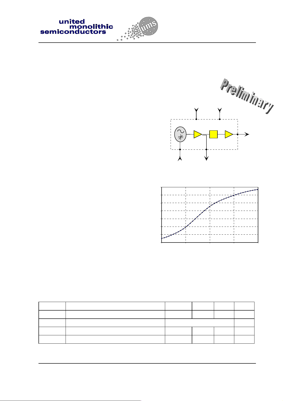
+V -V
F_VCO = F_out/3
x3
V_tune
Multifunction block diagram
40
39,5
39
38,5
38
37,5
Output frequency (GHz)
37
36,5
0 0,5 1 1,5 2
Typical tuning characteristic
VCO_out_aux
Tuning voltage (V)
RF_out
(F_out)
Main Characteristics
Tamb = +25°C
Symbol Parameter Min Typ Max Unit
F_out Out put centre frequency 38 38.25 38.5 GHz
F_vco Oscillator frequency F_out/3
F_tune1 Output frequency tuning range 1.5 3 GHz
Pout Output power 5 7 dBm
ESD Protections : Electrostatic discharge sensitive device observe handling precautions !
Ref. : DSCHV22431074 -15-Mar.-01 1/6 Specifications subject to change without notic e
united monolithic semiconductors S.A.S.
Route Départementale 128 - B.P.46 - 91401 Orsay Cedex France
Tel. : +33 (0)1 69 33 03 08 - Fax : +33 (0)1 69 33 03 09
Page 2
CHV2243
Q-band VCO
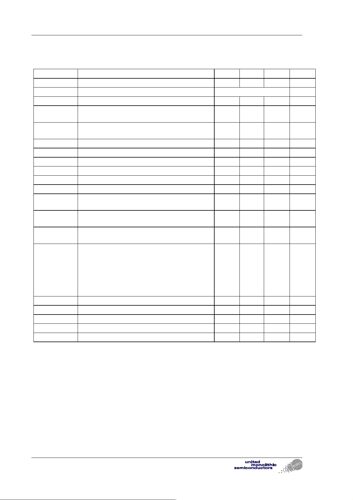
Electrical Characteristics
Full temperature range, used accor ding to section “Typical assembly and bias configurat ion”
Symbol Parameter Min Typ Max Unit
F_out Output centre frequency 38 38.25 38.5 GHz
F_vco VCO frequency F_out/3
F_tune1 Maximum f r equency tuning range (@ F_out) 1.5 3 4 GHz
F_tune2 Specif ied frequency tuning range (@ F_out)
(1)
∆F_tune2(T)
P_out Output power on RF_out port 5 7 12 dBm
H1 Sub-harmonics rejection (Fout/3) (2) -16 -11 dBc
H2 Sub-harmonics rejection (2*Fout/3) (2) -17 -12 dBc
P_VCO VCO output power on VCO_out_aux port (4) tbd
V_tune Control voltage range 0.5-1 0 - 2 V
F_slope Fr equency tuning slope (2) 1000 2800 4500 MHz/v
∆F_slope(T)
P_V+ Frequency pushing vs positive supply
P_V- Frequency pushing vs negative supply
PN Phase noise (given at F_out) (2)
+V Positive supply voltage (3) 4.4 4.5 4.6 V
+I Positive supply current 130 180 mA
-V Negative supply voltage (3) -4.6 -4.5 -4.4 V
-I Negative supply current 4 8 mA
Top Operating temperature r ange -40 +100 °C
Maximum variation of Frequency over
temperature (2)
Maximum variation of Frequency tuning
slope over temperature (2)
voltage (2)
voltage (2)
@ 1kHz
@ 10kHz
@ 100kHz
@ 200kHz
@ 1MHz
200 300 500 MHz
-300 +300 MHz
-26 +34 %
150 450 MHz/v
80 250 MHz /v
-5
-35
-65
-73
-92
+5
-25
-55
-63
-82
dBc/Hz
(1) F_tune2 is the frequency tuning range relative to the specified parameters, this
frequency tuning range has to be inside 38 to 38.5GHz.
(2) Specified within F_tune2
(3) Negative supply voltage must be applied at least 1µs before positive supply
voltage
(4) This output is optional, it can be not connected
Ref. : DSCHV22431074 -15-Mar.-01 2/6 Specifications subject to change without notic e
Route Départementale 128 , B.P.46 - 91401 ORSAY Cedex - FRANCE
Tel.: +33 (0)1 69 33 03 08 - Fax : +33 (0)1 69 33 03 09
Page 3

Q-band VCO
CHV2243
Absolute Maximum Ratings (1)
Symbol Parameter Values Unit
V_tune Tuning voltage 2.5 V
+V Positive supply voltage 5 V
-V Negative supply voltage -5 V
+I Positive supply current 250 mA
-I Negative supply current 15 mA
Tstg Storage temperature rang e -55 to +155 °C
(1) Operation of this device above anyone of these parameters may cause permanent damage.
Ref. : DSCHV22431074 -15-Mar.-01 3/6 Specifications subject to change without notic e
Route Départementale 128 , B.P.46 - 91401 ORSAY Cedex - FRANCE
Tel.: +33 (0)1 69 33 03 08 - Fax : +33 (0)1 69 33 03 09
Page 4

CHV2243
Chip Mechanical Data and Pin References
200
350 500 650 800 950 1100 1250 1550 1850 2150 2355
Q-band VCO
1040
Origin 0,0
Layout 2410X1110
123456 78 9
15
70
1440
Unit = µm
External chip size (including saw streets) = 2480 x 1180 +/- 35
Chip thickness = 100 +/- 10
HF Pads (13) = 68 x 118
VCO_out_aux Pad = 100 x 100
DC/IF Pads = 100 x 100
10
11
12
13
14
615
Pin number Pin name Description
12, 14
Ground: should not be bonded. If r equired,
please ask for more information.
3
13
8, 10
5, 9
4, 6, 7, 11
1, 2
RF_out
+V
-V
V-tune
Ground (optional)
RF output port @38GHz
Positive supply voltage
Negative supply voltage
NC
Tuning voltage input ports (s hould be connect ed
together, see typical assembly and bias
configuration)
15
Ref. : DSCHV22431074 -15-Mar.-01 4/6 Specifications subject to change without notic e
Route Départementale 128 , B.P.46 - 91401 ORSAY Cedex - FRANCE
VCO_out_aux
Tel.: +33 (0)1 69 33 03 08 - Fax : +33 (0)1 69 33 03 09
Auxiliary VCO output at 12.7GHz (F_out / 3) (optional)
Page 5

Q-band VCO
Typical Assembly and Bias Configuration
DC and control lines
-V +V
>= 120pF
V-tune
CHV2243
12345678 9
10 11
12
µ-strip line
13
14
L_out
15
L_aux
µ-stri p line
This drawing shows an example of assembly and bias configuration. All the
transistors are internally self biased. The posit ive and negative voltages can be
respectively connected together (see drawing) according to the recommended
values given in the electrical characteristics table.
For the RF pads the equivalent wire bonding inductance (diameter=25µm) has t o
be according to the following recomm endat ion.
Port Equivalent inductance
(nH)
Approximated wire
length (mm)
RF_out (13) L_out = 0.28 0.35
VCO_out_aux (15) L_aux = 0.4 0.5
For a micro-strip configuration a hole in the substrate is recom mended for chip
assembly.
Ref. : DSCHV22431074 -15-Mar.-01 5/6 Specifications subject to change without notic e
Route Départementale 128 , B.P.46 - 91401 ORSAY Cedex - FRANCE
Tel.: +33 (0)1 69 33 03 08 - Fax : +33 (0)1 69 33 03 09
Page 6

CHV2243
Q-band VCO
Ordering Information
Chip form : CHV2243-99F/00
Information furnished is believed to be accurate and reliable. However united monolithic semiconductors
S.A.S. assumes no responsibility for the consequences of use of such information nor for any infringement of
patents or other rights of third parties which may result from its use. No license is granted by implication or
otherwise under any patent or patent rights of united monolithic semiconductors S.A.S.. Specifications
mentioned in this publication are subject to change without notice. This publication supersedes and replaces all
information previously supplied. United monolithic semiconductors S.A.S. products are not authorised for use
as critical components in life support devices or systems without express written approval from united
monolithic semiconductors S.A.S.
Ref. : DSCHV22431074 -15-Mar.-01 6/6 Specifications subject to change without notic e
Route Départementale 128 , B.P.46 - 91401 ORSAY Cedex - FRANCE
Tel.: +33 (0)1 69 33 03 08 - Fax : +33 (0)1 69 33 03 09
 Loading...