

Page 1
CHV2241
K-band Oscillator with integrated Q-band Harmonic
Mixer
GaAs Monolithic Microwave IC
Description
The CHV2241 is a monolithic multifunction
proposed for frequency generation and
transposition. It integrates a K-band oscillator, a
Q-band harmonic mixer and buffer amplifiers.
For performance optimisation, an external port
(ERC) allows a passive resonator coupling to
the oscillator (at half output frequency). All the
active devices are internally self biased.
The circuit is manufactured with the P-HEMT
process : 0.25µm gate length, via holes through
the substrate, air bridges and electron beam
gate lithography.
It is available in chip form.
Main Features
n K-band Oscillator + Q-band harmonic
mixer
n External resonator for centre f requency
control and phase noise optimisation
n High quality oscillator when coupled to
a dielectric resonator
n Low conversion loss
n High temperature rang e
n On chip self biasing
n Automatic assembly oriented
n Chip size 1.82 x 0.97 x 0.1 mm
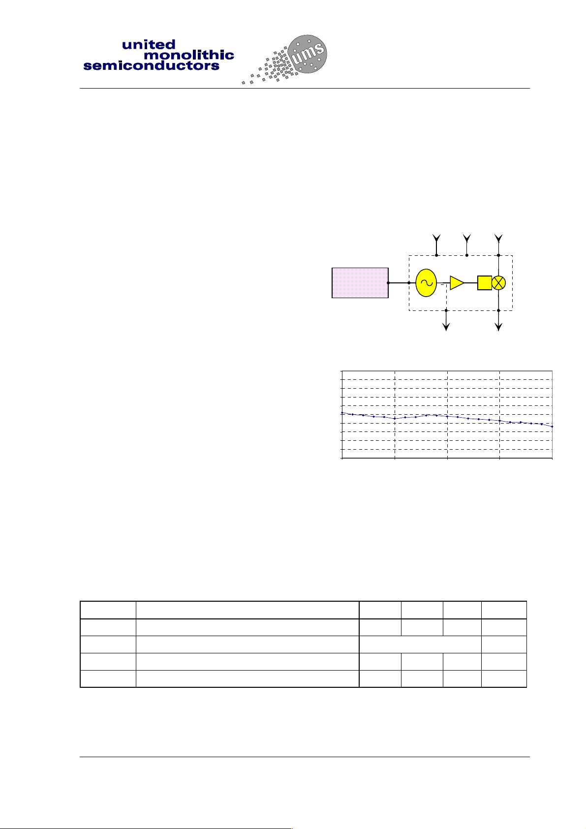
F_lo = (F_rf - F_if)/2
HIGH Q
RESONATOR
Multifunction block diagram
0
-1
-2
-3
-4
-5
-6
-7
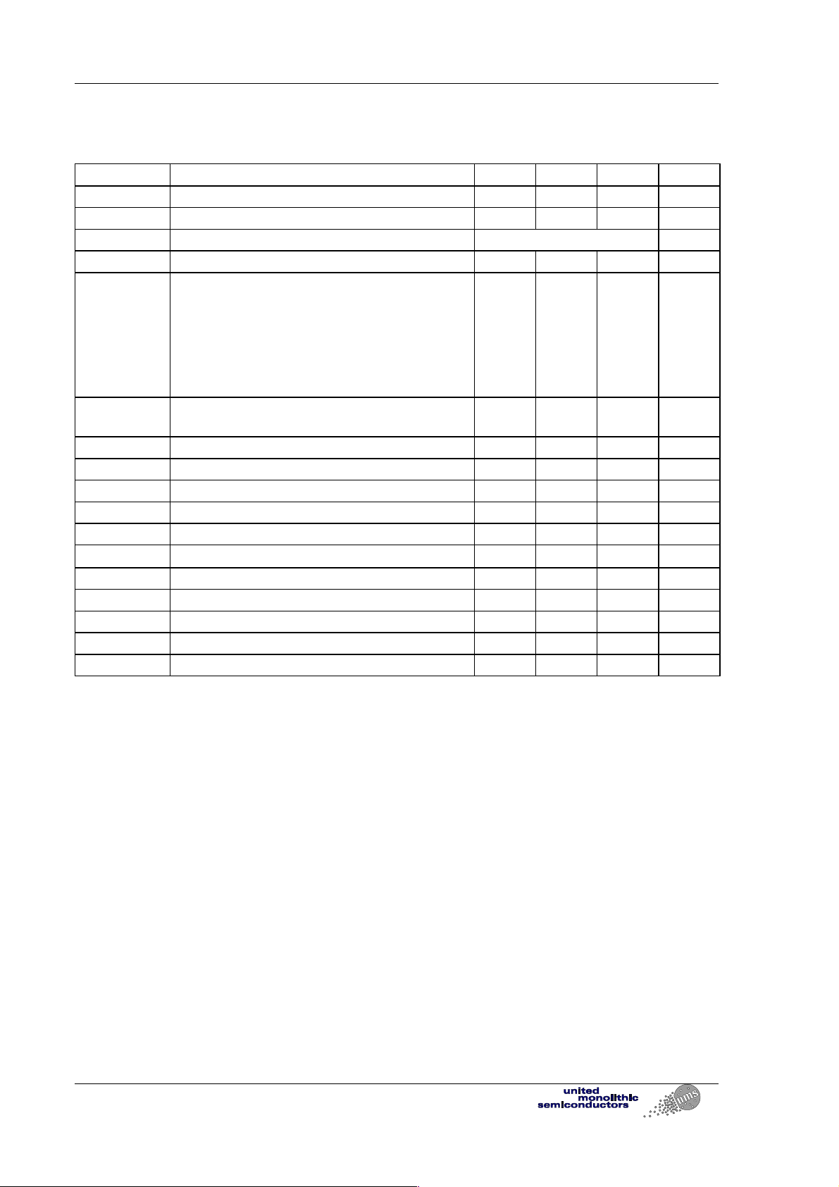
Conversion loss (dB)
-8
-9
-10
37 37,5 38 38,5 39
Typical conversion loss characteristic
+V -V RF
ERC
LO_out_aux
RF Frequency (GHz)
x2
IF
Main Characteristics
Tamb = +25°C
Symbol Parameter Min Typ Max Unit
F_rf RF frequency 37.5 38.25 39 GHz
F_lo Oscillator frequency (F_rf - F_if) / 2
Pn Oscillator phase noise @ 100kHz (38GHz) -100 dBc/Hz
Lc Conversion loss 7 dB
ESD Protections : Electrostatic discharge sensitive device observe handling precautions !
Ref. : DSCHV22411074 -15-Mar.-01 1/8 Specifications subject to change without notic e
Route Départementale 128 - B.P .46 - 91401 Orsay Cedex France
united monolithic s emiconductors S.A .S.
Tel. : +33 (0)1 69 33 03 08 - Fax : +33 (0)1 69 33 03 09
Page 2
CHV2241
K-band Oscillator / Q-band Mixer
Electrical Characteristics
Full temperature range, used accor ding to section “Typical assembly and bias configurat ion”
Symbol Parameter Min Typ Max Unit
F_rf RF frequency 37.5 38.25 39 GHz
F_if IF frequency 0.1 1.5 GHz
F_lo Oscillator frequency (1) (F_rf - F_if) / 2
P_lo Auxiliary LO output power (optional) -15 -8 -4 dBm
Pn Phase noise (given at RF frequency) (2)
@ 1kHz
@ 10kHz
@ 100kHz
@ 200kHz
@ 1MHz
P_V+ Frequency pushing vs positive supply
voltage
Lc Conversion loss 3 7 11 dB
P_1dB_rf RF input power at 1dB -13 -8 0 dBm
Plolk_if LO leakage at IF port (3) -25 -18 dBm
P2lo_rf 2LO leakage at RF por t (3) -40 -30 dBm
VSWR_rf VSWR at RF input port 2:1 2. 5:1
IMP_if IF load impedance 50
+V Positive supply voltage (4) 4.4 4.5 4.6 V
+I Positive supply current 50 90 mA
-V Negative supply voltage (4) -4.6 -4.5 -4.4 V
-I Negative supply current 6 10 mA
Top Operating temper at ure range -40 +100 °C
-45
-78
-105
-114
-129
300 1000 kHz/v
-35
-68
-95
-104
-119
dBc/Hz
Ω
(1) The centre frequency is given by the external passive resonator.
See part “Proposed external high Q resonator“ for frequency temperature drift
example.
DRO frequency long term stability is DR environment stability dependant
(hermeticity …).
(2) This characteristic depends on the external resonator Q, the given performance has
been obtained by using an external dielectric resonator ( see section “Proposed External
High Q resonator”)
(3) Without external filtering
(4) Negative supply voltage must be applied at least 1us before positive supply
voltage.
Ref. : DSCHV22411074 -15-Mar.-01 2/8 Specifications subj ect to change without notice
Route Départementale 128 , B.P.46 - 91401 ORSAY Cedex - FRANCE
Tel.: +33 (0)1 69 33 03 08 - Fax : +33 (0)1 69 33 03 09
Page 3
K-band Oscillator / Q-band Mixer
CHV2241
Absolute Maximum Ratings (1)
Symbol Parameter Values Unit
P_rf Maximum RF input power (2) 7 dBm
+V Positive supply voltage 5 V
-V Negative supply voltage -5 V
+I Positive supply current 100 mA
-I Negative supply current 15 mA
Tstg Storage temperature rang e -55 to +155 °C
(1) Operation of this device above anyone of these parameters may cause permanent damage.
(2) CW mode.
Ref. : DSCHV22411074 -15-Mar.-01 3/8 Specifications subj ect to change without notice
Route Départementale 128 , B. P.46 - 91401 ORSAY Cedex - FRANCE
Tel.: +33 (0)1 69 33 03 08 - Fax : +33 (0)1 69 33 03 09
Page 4

CHV2241
K-band Oscillator / Q-band Mixer
Chip Mechanical Data and Pin References
4
3
2
1
Unit = µm
External chip size (including saw streets)= 1820 x 970 +/- 35
Chip thickness = 100 +/- 10
HF Pads (2, 6) = 68 x 118
DC/IF Pads (+auxiliary LO output) = 100 x 100
5
6
7
8910111213
Pin number Pin name Description
1,3,5,7,8
2ERC
4 LO_OUT_AUX
6RF
9IF
10
11 -V
12,13 +V
Ref. : DSCHV22411074 -15-Mar.-01 4/8 Specifications subj ect to change without notice
Route Départementale 128 , B.P.46 - 91401 ORSAY Cedex - FRANCE
Tel.: +33 (0)1 69 33 03 08 - Fax : +33 (0)1 69 33 03 09
Ground : should not be bonded. If r equired,
please ask for more information
External Resonator Coupling Port
Oscillator auxiliary output port (optional)
RF input port
IF output port
NC
Negative supply voltage
Positive supply voltage
Page 5

K-band Oscillator / Q-band Mixer
Typical Assembly and Bias Configuration
4
CHV2241
µ-strip line
L_erc
3
2
1
8910111213
>= 120pF >= 120pF
-V+V IF
DC and control lines
5
6
7
µ-strip line
L_rf
This drawing shows an example of assembly and bias configuration. All the
transistors are internally self biased. The posit ive and negative voltages can be
respectively connected together (see drawing) according to the recommended
values given in the electrical characteristics table.
For the RF pads the equivalent wire bonding inductances (diameter=25µm) have
to be according to the following recom m endation.
Port Equivalent inductance
(nH)
Approximative wire
length (mm)
ERC (2) L_erc = 0.4 0.5
LO_OUT_AUX (4)
Not critical , < 1nH
Optional
RF (6) L_rf = 0.28 0.35
For a micro-strip configuration a hole in the substrate is recom mended for chip
assembly.
Ref. : DSCHV22411074 -15-Mar.-01 5/8 Specifications subj ect to change without notice
Route Départementale 128 , B. P.46 - 91401 ORSAY Cedex - FRANCE
Tel.: +33 (0)1 69 33 03 08 - Fax : +33 (0)1 69 33 03 09
Page 6

CHV2241
K-band Oscillator / Q-band Mixer
Proposed external high Q resonator
This chip has been especially designed to be coupled to a high Q dielectric
resonator (For example typical Q. @ 10 GHz=24000 for MURATA
/DRD036EC016). The resonance is given by a dielectric cylinder coupled to a
50Ω line. The size of the resonator gives the centre frequency and the space
between the resonator and the line gives the loaded quality fact or. The f ollowing
drawing shows an example of external configuration. As it is the assembly of a
test fixture all the biases are used and the auxiliary LO output is connected.
However, for a fixed application the configuration given in the previous section
can by applied.
Alumina substrate : thickness=250µm
Dielectric
resonator
50 Ohm resistance
d
via hole
Additional information
n Resonator reference example = MURATA /DRD036EC016. Other
n Temperature drift : For example, in the –40 to +100°C temperature
n Resonator coupling : d=0.3mm , l=1.5mm. T hese values have been
n 50ΩΩΩΩ line width on alumina (heigth=0.25mm) = 0.238mm
n Cavity size (mm) : 18 x 17 x 7
2l
kind of resonators can be used (from TEKELEC or TRANS-TECH).
The temperature coefficient has to be chosen according to the
environment.
range, the frequency drift @ 38GHz is 12 MHz with the MURATA /
DRD036EC016 resonator.
used in the test fixture, of course they can be modified if the
environment is different .
3l
Ref. : DSCHV22411074 -15-Mar.-01 6/8 Specifications subj ect to change without notice
Route Départementale 128 , B.P.46 - 91401 ORSAY Cedex - FRANCE
Tel.: +33 (0)1 69 33 03 08 - Fax : +33 (0)1 69 33 03 09
Page 7

K-band Oscillator / Q-band Mixer
CHV2241
External Resonator Coupling Informati on
The external resonator has to be an equivalent series resonance. However, this
impedance must be compatible to the negative impedance of the oscillator ERC
port in order to obtain the oscillation conditions and to avoid parasit ic oscillat ions.
Typical impedance of ERC port (Zerc) is given in the following table. The
diagram shows this impedance in a wider band. These values don’t include the
wire bonding (self L_erc given in the previous section).
The recommended external resonator properties are:
• series equivalent resonance
• highest possible Q (dielectric resonator, cavity ...) if no tuning
bandwidth required
• resistance at resonant frequency lower than 20ΩΩΩΩ
• out-off band impedance has to be designed to avoid parasitic oscillation.
Ref. : DSCHV22411074 -15-Mar.-01 7/8 Specifications subj ect to change without notice
Route Départementale 128 , B. P.46 - 91401 ORSAY Cedex - FRANCE
Tel.: +33 (0)1 69 33 03 08 - Fax : +33 (0)1 69 33 03 09
Page 8

CHV2241
K-band Oscillator / Q-band Mixer
Ordering Information
Chip form : CHV2241-99F/00
Information furnished is believed to be accurate and reliable. However united monolithic semiconductors
S.A.S. assumes no responsibility for the consequences of use of such information nor for any infringement of
patents or other rights of third parties which may result from its use. No license is granted by implication or
otherwise under any patent or patent rights of united monolithic semiconductors S.A.S.. Specifications
mentioned in this publication are subject to change without notice. This publication supersedes and replaces all
information previously supplied. United monolithic semiconductors S.A.S. products are not authorised for use
as critical components in life support devices or systems without express written approval from united
monolithic semiconductors S.A.S.
Ref. : DSCHV22411074 -15-Mar.-01 8/8 Specifications subj ect to change without notice
Route Départementale 128 , B.P.46 - 91401 ORSAY Cedex - FRANCE
Tel.: +33 (0)1 69 33 03 08 - Fax : +33 (0)1 69 33 03 09
 Loading...