

Page 1
CHRONTEL
Digital PC to TV Encoder
CH7003B
Features
• Input data path handles 8, 12, or 16-bit words in
multiplexed or non-multiplexed form
• Decodes pixel data in YCrCb (CCIR601 or 656) or
RGB (15, 16 or 24-bit) formats
• Supports 640x480, 640x400, 720x400, 800x600 and
512x384 input resolutions
• Adjustable underscan for most modes† ¥
• High quality 4-line flicker filtering †
• High resolution on-chip PLL
• Fully programmable through I2C port
• Supports NTSC, NTSC-EIA (Japan), and PAL (B, D,
G, H, I, M and N) TV formats
• Provides Composite, S-Video and SCART outputs
• CCIR624-3 compliant (see exceptions)
• Auto-detection of TV presence
• Sub-carrier genlock and dot crawl control
• Programmable power management
• 9-bit video DAC outputs
• Complete Windows and DOS driver software
• Offered in a 44-pin PLCC, 44-pin TQFP
† Patent number 5,781,241
General Description
Chrontel’s CH7003 digital PC to TV encoder is a standalone integrated circuit which provides a PC 99 compliant
solution for TV output. It provides a universal digital input
port to accept a pixel data stream from a compatible VGA
controller (or equivalent) and converts this directly into
NTSC or PAL TV format, with simultaneous composite
and S-Video outputs.
This circuit integrates a digital NTSC/PAL encoder with 9bit DAC interface, and new adaptive flicker filter, and high
accuracy low-jitter phase locked loop to create outstanding
quality video. Through its TrueScaleTM scaling and deflickering engine, the CH7003 supports full vertical and
horizontal underscan capability and operates in 5 different
resolutions including 640x480 and 800x600.
A new universal digital interface along with full
programmability make the CH7003 ideal for system-level
PC solutions. All features are software programmable
through a standard I2C port, to enable a complete PC
solution using a TV as the primary display.
¥ Patent number 5,914,753
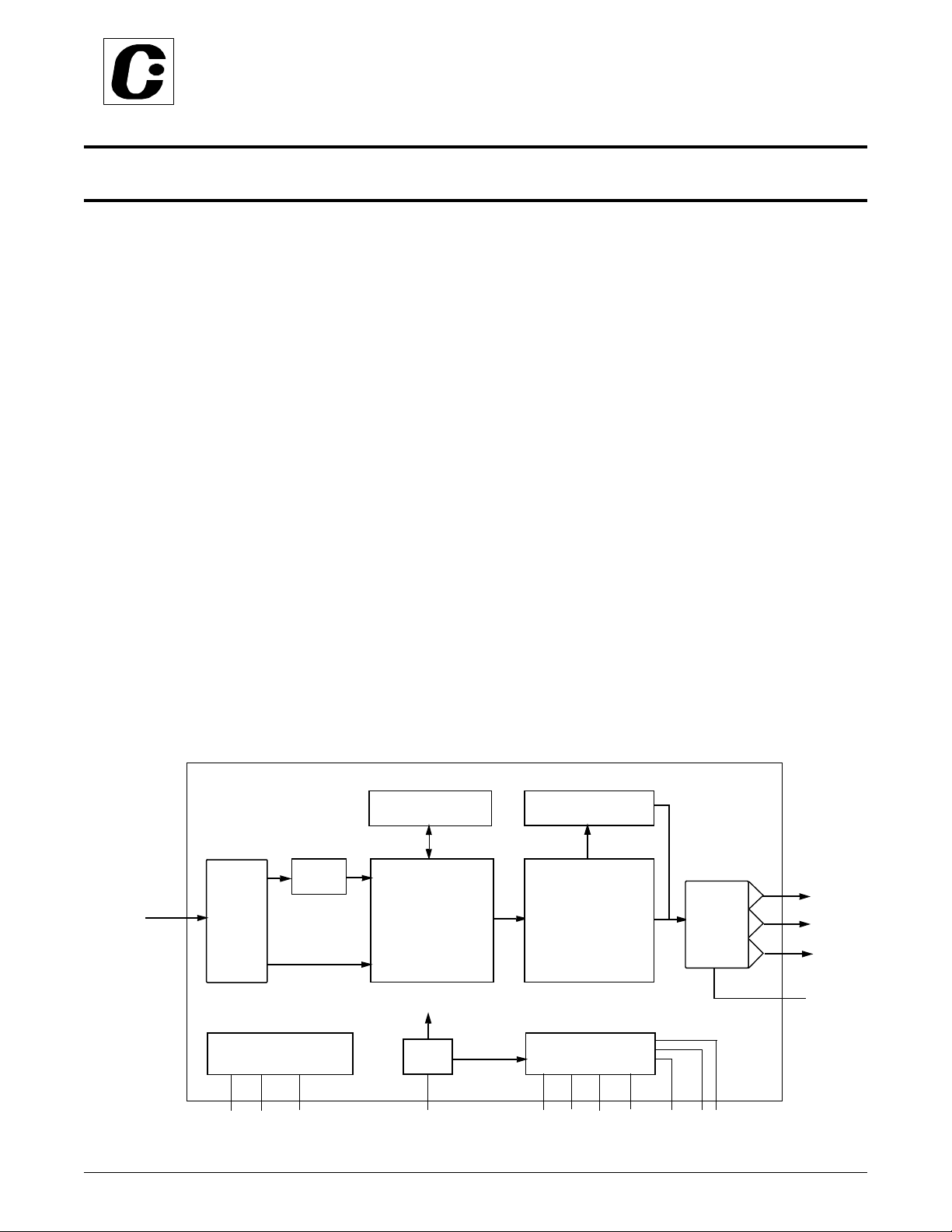
LINE
MEMORY
RGB-YUV
D[15:0
PIXEL DATA
]
CONVERTER
DIGITAL
INPUT
INTERFACE
I2C REGISTER & CONTROL
BLOCK
SC SD ADDR
TRUE SCALE
SCALING & DEFLICKERING
ENGINE
SYSTEM CLOCK
PLL
XCLK
Figure 1: Functional Block Diagram
201-0000-023 Rev 4.1, 8/2/99 1
YUV-RGB CONVERTER
NTSC/PAL
ENCODER
& FILTERS
TIMING & SYNC GENERATOR
V
XI XO/FIN
H
CSYNC
P-OUT
TRIPLE
DAC
BCO
Y/R
C/G
CVBS/G
RSET
Page 2
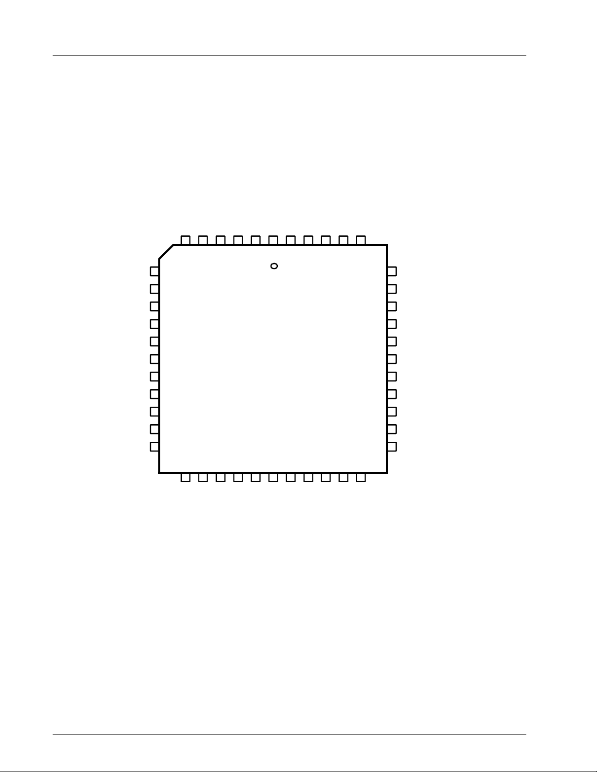
CHRONTEL CH7003B
D[2]
D[3]
D[1]
6
5
7
V
H
XCLK
DVDD
D[0]
4
3
2
1
P-OUT
DGND
BCO
AGND
44
43
42
41
40
39
XO/FIN
D[4]
D[5]
D[6]
DVDD
8
9
10
11
38
37
36
35
XI
AVDD
DVDD
ADDR
CHRONTEL
D[7] DGND
D[8]
D[9]
D[10]
D[11]
12
13
14
15
16
17
34
CH7003
18
19
20
21
22
D[12]
D[13]
D[14]
D[15]
DVDD
24
23
CSYNC
25
26
27
28
Y
C
GND
DGND
CVBS
33
32
31
30
29
SC
SDDGND]
VDD
RSET
GND
Figure 2: 44-pin PLCC
2 201-0000-023 Rev.4.1, 8/2/99
Page 3
CHRONTEL CH7003B
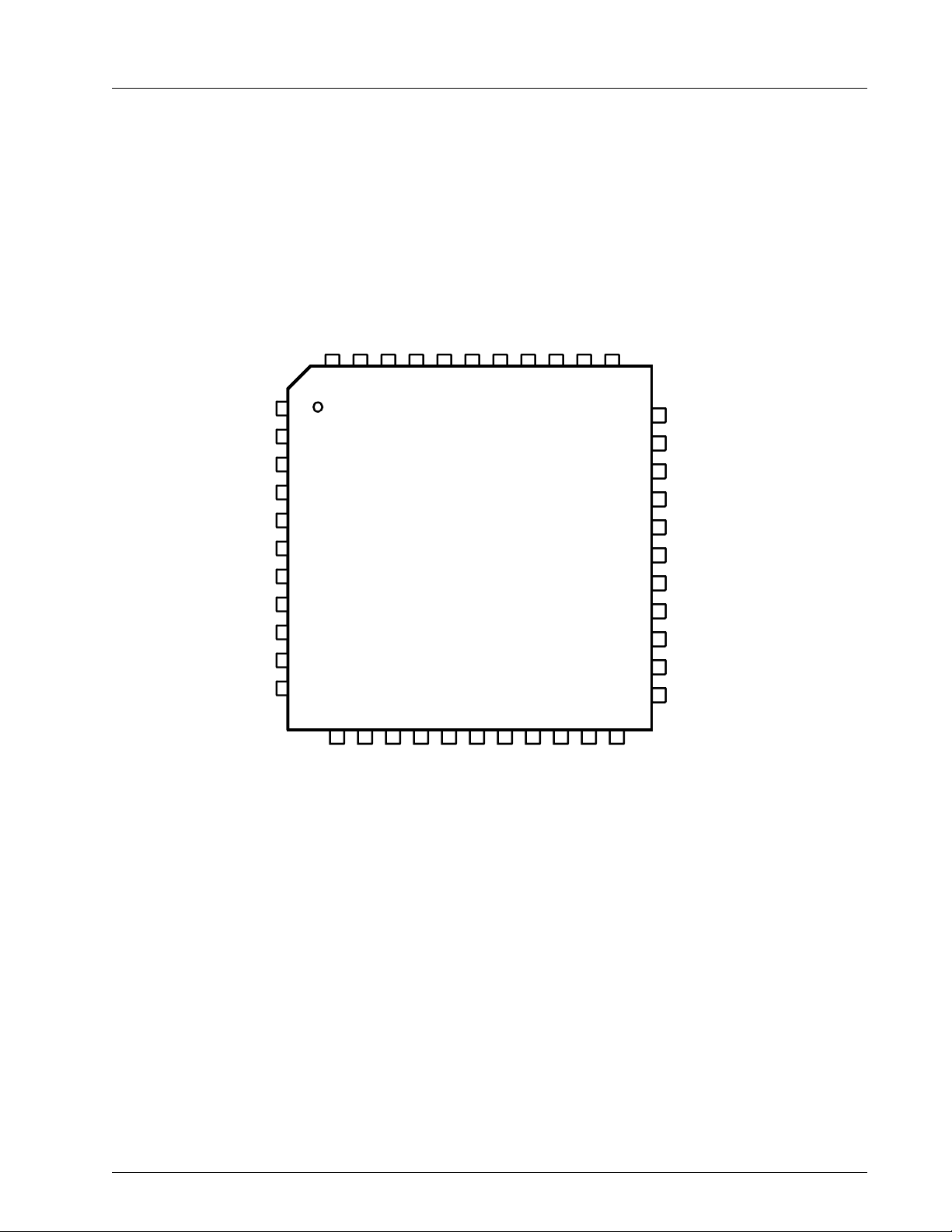
Figure 3: 44-pin TQFP
D[2]
D[3]
D[3]
D[4]
D[4]
D[5]
D[5]
D[6]
D[6]
DVDD
DVDD
D[7]
D[7]
D[8]
D[8]
DGND]
DGND]
D[9]
D[9]
D[10]
D[10]
D[11]
D[11]
1
2
3
4
5
6
7
8
9
10
11
D[1]
44
43
12
13
V
H
XCLK
DVDD
D[0]
42
41
40
39
P-OUT
38
37
CHRONTEL
CH7003
14
15
16
18
17
DGND
BCO
AGND
36
35
34
33
XO/FIN
XO/FIN
32
XI
XI
AVDD
31
AVDD
DVDD
30
DVDD
ADDR
29
ADDR
DGND
28
DGND
SC
27
SC
SD
26
SD
VDD
25
VDD
RSET
24
RSET
GND
23
GND
19
20
21
22
Y
C
D[12]
D[13]
D[14]
D[15]
DVDD
CSYNC
GND
DGND
CVBS
Figure 3: 44-PIN TQFP
201-0000-023 Rev 4.1, 8/2/99 3
Page 4
CHRONTEL CH7003B
Table 1. Pin Description
44-Pin
PLLC
21-15,
13-12,
10-4
43 37 Out P-OUT
1 39 In XCLK
3 41 In/Out V
2 40 In/Out H
41 35 Out BCO
38 32 In XI
39 33 In XO/FIN
30 24 In RSET
28 22 Out Y/R
27 21 Out C/G
44-Pin
TQFP
15,14,
13,12,
11,10,
9,7,6,4,
3,2,
1,44,43,
42
Type Symbol Description
In D15-D0
Digital Pixel Inputs
These pins accept digital pixel data streams with either 8, 12, or 16-bit
multiplexed or 16-bit non-multiplexed formats, determined by the input
mode setting (see Registers and Programming section). Inputs D0 - D7 are
used when operating in 8-bit multiplexed mode. Inputs D0 - D11 are used
when operating in 12-bit mode. Inputs D0 - D15 are used when operating
in 16-bit mode. The data structure and timing sequence for each mode is
described in the section on Digital Video Interface.
Pixel Clock Output
The CH7003, operating in master mode, provides a pixel data clocking
signal to the VGA controller. This pin provides the pixel clock output signal
(adjustable as 1X, 2X or 3X) to the VGA controller (see the section on
Digital Video Interface and Registers and Programming for more details).
The capacitive loading on this pin should be kept to a minimum.
Pixel Clock Input
To operate in a pure master mode, the P-OUT signal should be connected
to the XCLK input pin. To operate in a pseudo-master mode, the P-OUT
clock is used as a reference frequency, and a signal locked to this output (at
1X, 1/2X, or 1/3X the P-OUT frequency) is input to the XCLK pin. To operate
in slave mode, the CH7003 accepts an external pixel clock input at this pin.
The capacitive loading on this pin should be kept to a minimum.
Vertical Sync Input/Output
This pin accepts the vertical sync signal from the VGA controller, or outputs
a vertical sync to the VGA controller. The capacitive loading on this pin
should kept to a minimum.
Horizontal Sync Input/Output
This pin accepts the horizontal sync from the VGA controller, or outputs a
horizontal sync to the VGA controller. The capacitive loading on this pin
should be kept to a minimum.
Buffered Clock Output
This pin provides a buffered output of the 14.31818 MHz crystal input
frequency for other devices and remains active at all times (including
power-down). The output can also be selected to be other frequencies (see
Registers and Programming).
Crystal Input
A parallel resonance 14.31818 MHz (± 50 ppm) crystal should be attached
between XI and XO/FIN. However, if an external CMOS clock is attached to
XO/FIN, XI should be connected to ground.
Crystal Output or External Fref
A 14.31818 MHz (± 50 ppm) crystal may be attached between XO/FIN and
XI. An external CMOS compatible clock can be connected to XO/FIN as an
alternative.
Reference Resistor
A 360 Ω resistor with short and wide traces should be attached between
RSET and ground. No other connections should be made to this pin.
Luminance Output
A 75 Ω termination resistor with short traces should be attached between Y
and ground for optimum performance. In normal operating modes other
than SCART, this pin outputs the luma video signal. In SCART mode, this
pin outputs the red signal.
Chrominance Output
A 75 Ω termination resistor with short traces should be attached between C
and ground for optimum performance. In normal operating modes other
than SCART, this pin outputs the chroma video signal. In SCART mode,
this pin outputs the green signal.
4 201-0000-023 Rev.4.1, 8/2/99
Page 5

CHRONTEL CH7003B
Table 1. Pin Description (continued)
44-Pin
PLLC
26 20 Out CVBS/B
23 17 Out CSYNC
32 26 In/Out SD
33 27 In SC
35 29 In ADDR
40 34 Power AGND
37 31 Power AVDD
31 25 Power VDD
29, 25 19,23 Power GND
44, 36,
22, 11
42, 34,
24, 14
N/A N/A Out R
N/A N/A Out G
N/A N/A Out B
44-Pin
TQFP
5,16,
30,38
8, 18,
28, 36
Type Symbol Description
Power DVDD
Power DGND
Composite Video Output
A 75 Ω termination resistor with short traces should be attached between
CVBS and ground for optimum performance. In normal operating modes
other than SCART, this pin outputs the composite video signal. In SCART
mode, this pin outputs the blue signal.
Composite Sync Output
A 75 Ω termination resistor with short traces should be attached between
CSYNC and ground for optimum performance. In SCART mode, this pin
outputs the composite sync signal.
Serial Data (External pull-up required)
This pin functins as SD, the serial data pin of the I2C interface port (see the
I 2C Port Operation section for details).
Serial Clock (Internal pull-up)
This pin functions as the serial clock pin of the I2C interface port (see the
I 2C Port Operation section for details).
I2C Address Select (Internal pull-up)
This pin is the I2C Address Select, which corresponds to bits 1 and 0 of the
I2C device address (see the I 2C Port Operation section for details), creating
an address selection as follows:
ADDR I2C Address Selected
1 1110101 = 75H = 117
0 1110110 = 76H = 118
Analog ground
These pins provide the ground reference for the analog section of CH7003,
and MUST be connected to the system ground, to prevent latchup.
Analog Supply Voltage
These pins supply the 5V power to the analog section of the CH7003.
DAC Power Supply
These pins supply the 5V power to CH7003’s internal DACs.
DAC Ground
These pins provide the ground reference for CH7003’s internal DACs.
Digital Supply Voltage
These pins supply the 3.3V power to the digital section of CH7003.
Digital Ground
These pins provide the ground reference for the digital section of CH7003,
and MUST be connected to the system ground to prevent latchup.
R (Red) Component Output
This pin provides the analog Red component of the digital RGB input in the
RGB Pass-Through mode.
G (Green) Component Output
This pin provides the analog Green component of the digital RGB input in
the RGB Pass-Through mode.
B (Blue) Component Output
This pin provides the analog Blue component of the digital RGB input in the
RGB Pass-Though mode.
201-0000-023 Rev 4.1, 8/2/99 5
Page 6
CHRONTEL CH7003B
Digital Video Interface
The CH7003 digital video interface provides a flexible digital interface between a computer graphics controller and
the TV encoder IC, forming the ideal quality/cost configuration for performing the TV-output function. This digital
interface consists of up to 16 data signals and 4 control signals, all of which are subject to programmable control
through the CH7003 register set. This interface can be configured as 8, 12 or 16-bit inputs operating in either
multiplexed mode or 16-bit input operation in de-multiplexed mode. It will also accept either YCrCb or RGB (15,
16 or 24-bit) data formats. A summary of the data format modes is as follows:
Table 2. Input Data Formats
Bus Width Transfer Mode Color Space and Depth Format Reference
16-bit Non-multiplexed RGB 16-bit 5-6-5 each word
15-bit Non-multiplexed RGB 15-bit 5-5-5 each word
16-bit Non-multiplexed YCrCb (24-bit) CbY0,CrY1...(CCIR656 style)
8-bit 2X-multiplexed RGB 15-bit 5-5-5 over two bytes
8-bit 2X-multiplexed RGB 16-bit 5-6-5 over two bytes
8-bit 3X-multiplexed RGB 24-bit 8-8-8 over three bytes
8-bit 2X-multiplexed YCrCb (24-bit) Cb,Y0,Cr,Y1,(CCIR656 style)
12-bit 2X-multiplexed RGB 24 8-8-8 over two words - ‘C’ version
12-bit 2X-multiplexed RGB 24 8-8-8 over two words - ‘I’ version
16-bit 2X-multiplexed RGB 24 (32) 8-8,8X over two words
The clock and timing signals used to latch and process the incoming pixel data is dependent upon the clock mode.
The CH7003 can operate in either master (the CH7003 generates a pixel frequency which is either returned as a
phase-aligned pixel clock or used directly to latch data), or slave mode (the graphics chip generates the pixel clock).
The pixel clock frequency will change depending upon the active image size (e.g., 640x480 or 800x600), the desired
ouput format (NTSC or PAL), and the amount of scaling desired. The pixel clock may be requested to be 1X, 2X or
3X the pixel data rate (subject to a 100 MHz frequency limitation). In the case of a 1X pixel clock the CH7003 will
automatically use both clock edges if a multiplexed data format is selected.
Sync Signals: Horizontal and vertical sync signals will normally be supplied by the VGA controller, but may be
selected to be generated by the CH7003. In the case of CCIR656 style input, embedded sync may also be used. In
each case, the horizontal timing signal (horizontal sync) must be derived from the pixel clock, with the period set to
exactly 8 times (9 times for 720x400 modes) the pixel clock period, times an integer value. Each line to be set, is set
up by the leading edge of Horizontal sync. The vertical timing signal must be able to be set to any integer number of
lines between 420 and 836.
Master Clock Mode: The CH7003 generates a clock signal (output at the P-OUT pin) which will be used by the
VGA controller as a frequency reference. The VGA controller will then generate a clock signal which will be input
via the XCLK input. This incoming signal will be used to latch (and de-multiplex, if required) incoming data. The
XCLK input clock rate must match the input data rate, and the P-OUT clock can be requested to be 1X, 2X or 3X
the pixel data rate. As an alternative, the P-OUT clock signal can also be used as the input clock signal (connected
directly to the XCLK input) to latch the incoming data. If this mode is used, the incoming data must meet setup and
hold times with respect to the XCLK input (with the only internal adjustment being XCLK polarity).
Slave Clock Mode: The VGA controller will generate a clock which will be input to the XCLK pin (no clock
signal will be output on the P-OUT pin). This signal must match the input data rate, must occur at 1X, 2X or 3X the
pixel data rate, and will be used to latch (and de-multiplex if required) incoming data. Also, the graphics IC
transmits back to the TV encoder the horizontal and vertical timing signals, and pixel data, each of which must meet
the specified setup and hold times with respect to the pixel clock.
Pixel Data: Active pixel data will be expected after a programmable number pixels times the multiplex rate after
the leading edge of Horizontal Sync. In other words, specifying the horizontal back porch value (as a pixel count),
plus horizontal sync width, will determine when the chip will begin to sample pixels.
6 201-0000-023 Rev.4.1, 8/2/99
Page 7
CHRONTEL CH7003B
Digital Video Interface (continued)
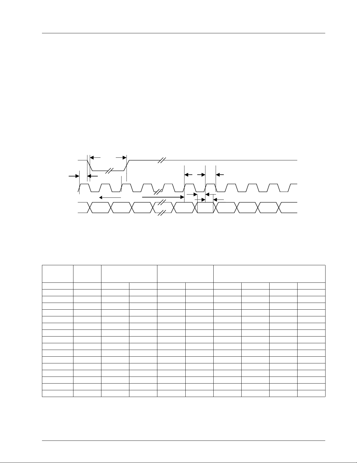
Non-multiplexed Mode
In the 15/16-bit mode shown in Figure4, the pixel data bus represents a 15/16-bit non-multiplexed data stream,
which contains either RGB or YCrCb formatted data. When operating in RGB mode, each 15/16-bit Pn value will
contain a complete pixel encoded in either 5-6-5 or 5-5-5 format. When operating in YCrCb mode, each 16-bit Pn
word will contain an 8-bit Y (luminance) value on the upper 8 bits, and an 8-bit C (color difference) value on the
lower 8 bits. The color difference will be transmitted at half the data rate of the luminance data, with the sequence
being set as Cb followed by Cr. The Cb and Cr data will be co-sited with the Y value transmitted with the Cb value,
with the data sequence described in Table3. The first active pixel is SAV pixels after the leading edge of horizontal
sync, where SAV is a bus-controlled register.
t
HSW
HSYNC
t
t
PH 1
PH
t
t
SP1
SP
t
t
HP
HP1
P2
P3 P4
P5
POut/
XCLK
Pixel
Data
t
t
HD
AVR
SAV
t
P
P 1
P0a P0b P1a P1b P2a P2b
P0
P1
Figure 4: Non-multiplexed Data Transfers
Table 3. 15/16-bit Non-multiplexed Data Formats
IDF#
Format
Pixel# P0 P1 P0 P1 P0 P1 P2 P3
Bus Data D[15] R0[4] R1[4] x x Y0[7] Y1[7] Y2[7] Y3[7]
D[14] R0[3] R1[3] R2[4] R3[4] Y0[6] Y1[6] Y2[6] Y3[6]
D[13] R0[2] R1[2] R2[3] R3[3] Y0[5] Y1[5] Y2[5] Y3[5]
D[12] R0[1] R1[1] R2[2] R3[2] Y0[4] Y1[4] Y2[4] Y3[4]
D[11] R0[0] R1[0] R2[1] R3[1] Y0[3] Y1[3] Y2[3] Y3[3]
D[10] G0[5] G1[5] R2[0] R3[0] Y0[2] Y1[2] Y2[2] Y3[2]
D[9] G0[4] G1[4] G2[4] G3[4] Y0[1] Y1[1] Y2[1] Y3[1]
D[8] G0[3] G1[3] G2[3] G3[3] Y0[0] Y1[0] Y2[0] Y3[0]
D[7] G0[2] G1[2] G2[2] G3[2] Cb0[7] Cr0[7] Cb2[7] Cr2[7]
D[6] G0[1] G1[1] G2[1] G3[1] Cb0[6] Cr0[6] Cb2[6] Cr2[6]
D[5] G0[0] G1[0] G2[0] G3[0] Cb0[5] Cr0[5] Cb2[5] Cr2[5]
D[4] B0[4] B1[4] B2[4] B3[4] Cb0[4] Cr0[4] Cb2[4] Cr2[4]
D[3] B0[3] B1[3] B2[3] B3[3] Cb0[3] Cr0[3] Cb2[3] Cr2[3]
D[2] B0[2] B1[2] B2[2] B3[2] Cb0[2] Cr0[2] Cb2[2] Cr2[2]
D[1] B0[1] B1[1] B2[1] B3[1] Cb0[1] Cr0[1] Cb2[1] Cr2[1]
D[0] B0[0] B1[0] B2[0] B3[0] Cb0[0] Cr0[0] Cb2[0] Cr2[0]
0
RGB 5-6-5
3
RGB 5-5-5
1
YCrCb (16-bit)
201-0000-023 Rev 4.1, 8/2/99 7
Page 8
CHRONTEL CH7003B
Digital Video Interface (continued)
When IDF = 1, (YCrCb 16-bit mode), H and V sync signals can be embedded into the data stream. In this mode, the
embedded sync will be similar to the CCIR656 convention (not identical, since that convention is for 8-bit data
streams), and the first byte of the ‘video timing reference code’ will be assumed to occur when a Cb sample would
occur – if the video stream was continuous. This is delineated in Table4 below.
Table 4. YCrCb Non-multiplexed Mode with Embedded Syncs
IDF#
Format
Pixel# P0 P1 P2 P3 P4 P5 P6 P7
Bus Data D[15] 0 S[7] Y0[7] Y1[7] Y2[7] Y3[7] Y4[7] Y5[7]
D[14] 0 S[6] Y0[6] Y1[6] Y2[6] Y3[6] Y4[6] Y5[6]
D[13] 0 S[5] Y0[5] Y1[5] Y2[5] Y3[5] Y4[5] Y5[5]
D[12] 0 S[4] Y0[4] Y1[4] Y2[4] Y3[4] Y4[4] Y5[4]
D[11] 0 S[3] Y0[3] Y1[3] Y2[3] Y3[3] Y4[3] Y5[3]
D[10] 0 S[2] Y0[2] Y1[2] Y2[2] Y3[2] Y4[2] Y5[2]
D[9] 0 S[1] Y0[1] Y1[1] Y2[1] Y3[1] Y4[1] Y5[1]
D[8] 0 S[0] Y0[0] Y1[0] Y2[0] Y3[0] Y4[0] Y5[0]
D[7] 1 0 Cb0[7] Cr0[7] Cb2[7] Cr2[7] Cb4[7] Cr4[7]
D[6] 1 0 Cb0[6] Cr0[6] Cb2[6] Cr2[6] Cb4[6] Cr4[6]
D[5] 1 0 Cb0[5] Cr0[5] Cb2[5] Cr2[5] Cb4[5] Cr4[5]
D[4] 1 0 Cb0[4] Cr0[4] Cb2[4] Cr2[4] Cb4[4] Cr4[4]
D[3] 1 0 Cb0[3] Cr0[3] Cb2[3] Cr2[3] Cb4[3] Cr4[3]
D[2] 1 0 Cb0[2] Cr0[2] Cb2[2] Cr2[2] Cb4[2] Cr4[2]
D[1] 1 0 Cb0[1] Cr0[1] Cb2[1] Cr2[1] Cb4[1] Cr4[1]
D[0] 1 0 Cb0[0] Cr0[0] Cb2[0] Cr2[0] Cb4[0] Cr4[0]
1
YCrCb 16-bit
In this mode, the S[7..0] byte contains the following data:
S[6] = F = 1 during field 2, 0 during field 1
S[5] = V = 1 during field blanking, 0 elsewhere
S[4] = H = 1 during EAV (the synchronization reference at the end of active video)
0 during SAV (the synchronization reference at the start of active video)
Bits S[7] and S[3..0] are ignored.
Multiplexed Mode
Each rising edge (or each rising and falling edge) of the XCLK signal will latch data from the graphics chip. The
multiplexed input data formats are shown in Figure5 and 6. The Pixel Data bus represents an 8-, 12-, or 16-bit
multiplexed data stream, which contains either RGB or YCrCb formatted data. In IDF settings of 2, 4, 5, 7, 8, and 9,
the input data rate is 2X PCLK, and each pair of Pn values (e.g., P0a and P0b) will contain a complete pixel,
encoded as shown in the tables below. When IDF = 6, the input data rate is 3X PCLK, and each triplet of Pn values
(e.g., P0a, P0b and P0c) will contain a complete pixel, encoded as shown in the tables below. When the input is
YCrCb, the color-difference data will be transmitted at half the data rate of the luminance data, with the sequence
being set as Cb, Y, Cr, Y where Cb0,Y0,Cr0 refers to co-sited luminance and color-difference samples — and the
following Y1 byte refers to the next luminance sample, per CCIR656 standards. However, the clock frequency is
dependent upon the current mode (not 27MHz, as specified in CCIR656.)
8 201-0000-023 Rev.4.1, 8/2/99
Page 9
CHRONTEL CH7003B
Digital Video Interface (continued)
t
HSW
HS
t
t
HD
P2
XCLK
DEC = 0
t
SP2
XCLK
DEC = 1
D[15:0] P0a P0b P1a P1b P2a P2b
Figure 5: Multiplexed Pixel Data Transfer Mode
t
PH2
t
HP2
t
t
SP2
HP2
t
t
SP2
HP2
Table 5. RGB 8-bit Multiplexed Mode
IDF#
Format
Pixel# P0a P0b P1a P1b P0a P0b P1a P1b
Bus Data D[7] G0[2] R0[4] G1[2] R1[4] G0[2] x G1[2] x
D[6] G0[1] R0[3] G1[1] R1[3] G0[1] R0[4] G1[1] R1[4]
D[5] G0[0] R0[2] G1[0] R1[2] G0[0] R0[3] G1[0] R1[3]
D[4] B0[4] R0[1] B1[4] R1[1] B0[4] R0[2] B1[4] R1[2]
D[3] B0[3] R0[0] B1[3] R1[0] B0[3] R0[1] B1[3] R1[1]
D[2] B0[2] G0[5] B1[2] G1[5] B0[2] R0[0] B1[2] R1[0]
D[1] B0[1] G0[4] B1[1] G1[4] B0[1] G0[4] B1[1] G1[4]
D[0] B0[0] G0[3] B1[0] G1[3] B0[0] G0[3] B1[0] G1[3]
7
RGB 5-6-5
8
RGB 5-5-5
Table 6. RGB 12-bit Multiplexed Mode
IDF#
Format
12-bit RGB (12-12)
Pixel# P0a P0b P1a P1b P0a P0b P1a P1b
Bus Data D[11] G0[3] R0[7] G1[3] R1[7] G0[4] R0[7] G1[4] R1[7]
D[10] G0[2] R0[6] G1[2] R1[6] G0[3] R0[6] G1[3] R1[6]
D[9] G0[1] R0[5] G1[1] R1[5] G0[2] R0[5] G1[2] R1[5]
D[8] G0[0] R0[4] G1[0] R1[4] B0[7] R0[4] B1[7] R1[4]
D[7] B0[7] R0[3] B1[7] R1[3] B0[6] R0[3] B1[6] R1[3]
D[6] B0[6] R0[2] B1[6] R1[2] B0[5] G0[7] B1[7] G1[7]
D[5] B0[5] R0[1] B1[5] R1[1] B0[4] G0[6] B1[4] G1[6]
D[4] B0[4] R0[0] B1[4] R1[0] B0[3] G0[5] B1[3] G1[5]
D[3] B0[3] G0[7] B1[3] G1[7] G0[0] R0[2] G1[0] R1[2]
D[2] B0[2] G0[6] B1[2] G1[6] B0[2] R0[1] B1[2] R1[1]
D[1] B0[1] G0[5] B1[1] G1[5] B0[1] R0[0] B1[1] R1[0]
D[0] B0[0] G0[4] B1[0] G1[4] B0[0] G0[1] B1[0] G1[1]
4
5
12-bit RGB (12-12)
201-0000-023 Rev 4.1, 8/2/99 9
Page 10
CHRONTEL CH7003B
Digital Video Interface (continued)
Table 7. RGB 16-bit Muliplexed Mode
IDF#
Format
Pixel# P0a P0b P1a P1b
Bus Data D[15] G0[7] A0[7] G1[7] A1[7]
D[14] G0[6] A0[6] G1[6] A1[6]
D[13] G0[5] A0[5] G1[5] A1[5]
D[12] G0[4] A0[4] G1[4] A1[4]
D[11] G0[3] A0[3] G1[3] A1[3]
D[10] G0[2] A0[2] G1[2] A1[2]
D[9] G0[1] A0[1] G1[1] A1[1]
D[8] G0[0] A0[0] G1[0] A1[0]
D[7] B0[7] R0[7] B1[7] R1[7]
D[6] B0[6] R0[6] B1[6] R1[6]
D[5] B0[5] R0[5] B1[5] R1[5]
D[4] B0[4] R0[4] B1[4] R1[4]
D[3] B0[3] R0[3] B1[3] R1[3]
D[2] B0[2] R0[2] B1[2] R1[2]
D[1] B0[1] R0[1] B0[1] R1[1]
D[0] B0[0] R0[0] B0[0] R1[0]
Note: The AX[7:0] data is ignored.
16-bit RGB (16-8)
2
Table 8. YCrCb Multiplexed Mode
IDF#
Format
Pixel# P0a P0b P1a P1b P2a P2b P3a P3b
Bus Data D[7] Cb0[7] Y0[7] Cr0[7] Y1[7] Cb2[7] Y2[7] Cr2[7] Y3[7]
D[6] Cb0[6] Y0[6] Cr0[6] Y1[6] Cb2[6] Y2[6] Cr2[6] Y3[6]
D[5] Cb0[5] Y0[5] Cr0[5] Y1[5] Cb2[5] Y2[5] Cr2[5] Y3[5]
D[4] Cb0[4] Y0[4] Cr0[4] Y1[4] Cb2[4] Y2[4] Cr2[4] Y3[4]
D[3] Cb0[3] Y0[3] Cr0[3] Y1[3] Cb2[3] Y2[3] Cr2[3] Y3[3]
D[2] Cb0[2] Y0[2] Cr0[2] Y1[2] Cb2[2] Y2[2] Cr2[2] Y3[2]
D[1] Cb0[1] Y0[1] Cr0[1] Y1[1] Cb2[1] Y2[1] Cr2[1] Y3[1]
D[0] Cb0[0] Y0[0] Cr0[0] Y1[0] Cb2[0] Y2[0] Cr2[0] Y3[0]
9
YCrCb 8-bit
When IDF = 9 (YCrCb 8-bit mode), H and V sync signals can be embedded into the data stream. In this mode, the
embedded sync will follow the CCIR656 convention, and the first byte of the “video timing reference code” will be
assumed to occur when a Cb sample would occur if the video stream was continuous. This is delineated in Table9.
10 201-0000-023 Rev.4.1, 8/2/99
Page 11
CHRONTEL CH7003B
Digital Video Interface (continued)
Table 9. YCrCb Multiplexed Mode with Embedded Syncs
IDF#
Format
Pixel# P0a P0b P1a P1b P2a P2b P3a P3b
Bus Data D[7] 1 0 0 S[7] Cb2[7] Y2[7] Cr2[7] Y3[7]
D[6] 1 0 0 S[6] Cb2[6] Y2[6] Cr2[6] Y3[6]
D[5] 1 0 0 S[5] Cb2[5] Y2[5] Cr2[5] Y3[5]
D[4] 1 0 0 S[4] Cb2[4] Y2[4] Cr2[4] Y3[4]
D[3] 1 0 0 S[3] Cb2[3] Y2[3] Cr2[3] Y3[3]
D[2] 1 0 0 S[2] Cb2[2] Y2[2] Cr2[2] Y3[2]
D[1] 1 0 0 S[1] Cb2[1] Y2[1] Cr2[1] Y3[1]
D[0] 1 0 0 S[0] Cb2[0] Y2[0] Cr2[0] Y3[0]
9
YCrCb 8-bit
In this mode, the S[7..0] byte contains the following data:
S[6] = F = 1 during field 2, 0 during field 1
S[5] = V = 1 during field blanking, 0 elsewhere
S[4] = H = 1 during EAV (the synchronization reference at the end of active video)
0 during SAV (the synchronization reference at the start of active video)
Bits S[7] and S[3..0] are ignored.
t
HSW
HSYNC
t
HD
t
P3
t
PH3
POut/
XCLK
t
Pixel
D[7:0]
Data
SP3
P0a P0b P0c P1a P1b P1c
t
HP3
Figure 6: Multiplexed Pixel Data Transfer Mode (IDF = 6)
Table 10. RGB 8-bit Multiplexed Mode (24-bit Color)
IDF#
Format
Pixel# P0a P0b P0c P1a P1b P1c P2a P2b P2C
Bus Data D[7] B0[7] G0[7] R0[7] B1[7] G1[7] R1[7] B2[7] G2[7] R2[7]
D[6] B0[6] G0[6] R0[6] B1[6] G1[6] R1[6] B2[6] G2[6] R2[6]
D[5] B0[5] G0[5] R0[5] B1[5] G1[5] R1[5] B2[5] G2[5] R2[5]
D[4] B0[4] G0[4] R0[4] B1[4] G1[4] R1[4] B2[4] G2[4] R2[4]
D[3] B0[3] G0[3] R0[3] B1[3] G1[3] R1[3] B2[3] G2[3] R2[3]
D[2] B0[2] G0[2] R0[2] B1[2] G1[2] R1[2] B2[2] G2[2] R2[2]
D[1] B0[1] G0[1] R0[1] B1[1] G1[1] R1[1] B2[1] G2[1] R2[1]
D[0] B0[0] G0[0] R0[0] B1[0] G1[0] R1[0] B2[0] G2[0] R2[0]
201-0000-023 Rev 4.1, 8/2/99 11
6
RGB 8-bit
Page 12

CHRONTEL CH7003B
Functional Description
The CH7003 is a TV-output companion chip to graphics controllers providing digital output in either YUV or RGB
format. This solution involves both hardware and software elements which work together to produce an optimum
TV screen image based on the original computer generated pixel data. All essential circuitry for this conversion are
integrated on-chip. On-chip circuitry includes memory, memory control, scaling, PLL, DAC, filters, and
NTSC/PAL encoder. All internal signal processing, including NTSC/PAL encoding, is performed using digital
techniques to ensure that the high-quality video signals are not affected by drift issues associated with analog
components. No additional adjustment is required during manufacturing.
CH7003 is ideal for PC motherboards, web browsers, or VGA add-in boards where a minimum of discrete support
components (passive components, parallel resonance 14.31818 MHz crystal) are required for full operation.
Architectural Overview
The CH7003 is a complete TV output subsystem which uses both hardware and software elements to produce an
image on TV which is virtually identical to the image that would be displayed on a monitor. Simply creating a
compatible TV output from a VGA input involves a relatively straightforward process. This process includes a
standard conversion from RGB to YUV color space, converting from a non-interlaced to an interlaced frame
sequence, and encoding the pixel stream into NTSC or PAL compliant format. However, creating an optimum
computer-generated image on a TV screen involves a highly sophisticated process of scaling, deflickering, and
filtering. This results in a compatible TV output that displays a sharp and subtle image, of the right size, with
minimal artifacts from the conversion process.
As a key part of the overall system solution, the CH7003 software establishes the correct framework for the VGA
input signal to enable this process. Once the display is set to a supported resolution (either 640x480 or 800x600),
the CH7003 software may be invoked to establish the appropriate TV output display. The software then programs
the various timing parameters of the VGA controller to create an output signal that will be compatible with the
chosen resolution, operating mode, and TV format. Adjustments performed in software include pixel clock rates,
total pixels per line, and total lines per frame. By performing these adjustments in software, the CH7003 can render
a superior TV image without the added cost of a full frame buffer memory – normally used to implement features
such as scaling and full synchronization.
The CH7003 hardware accepts digital RGB or YCrCb inputs, which are latched in synchronization with the pixel
clock. These inputs are then color-space converted into YUV in 4-2-2 format and stored in a line buffer memory.
The stored pixels are fed into a block where scan-rate conversion, underscan scaling and 2-line, 3-line, 4-line and 5line vertical flicker filtering are performed. The scan-rate converter transforms the VGA horizontal scan-rate to
either NTSC or PAL scan rates; the vertical flicker filter eliminates flicker at the output while the underscan scaling
reduces the size of the displayed image to fit onto a TV screen. The resulting YUV signals are filtered through
digital filters to minimize aliasing problems. The digital encoder receives the filtered signals and transforms them to
composite and S-Video outputs, which are converted by the three 9-bit DACs into analog outputs.
Color Burst Generation*
The CH7003 allows the sub-carrier frequency to be accurately generated from a 14.31818 MHz crystal oscillator,
leaving the sub-carrier frequency independent of the sampling rate. As a result, the CH7003 may be used with any
VGA chip (with an approprate digital interface) since the CH7003 sub-carrier frequency can be generated without
being dependent on the precise pixel rates of VGA controllers. This feature is a significant benefit, since even a
± 0.01% sub-carrier frequency variation may be enough to cause some television monitors to lose color lock.
In addition, the CH7003 has the capability to genlock the color burst signal to the VGA horizontal sync frequency,
which enables a fully synchronous system between the graphics controller and the television. When genlocked, the
CH7003 can also stop "dot crawl" motion (for composite mode operation, in NTSC modes) to eliminate the
annoyance of moving borders. Both of these features are under programmable control through the register set.
Display Modes
The CH7003 display mode is controlled by three independent factors: input resolution, TV format, and scale factor,
which are programmed via the display mode register. It is designed to accept input resolutions of 640x480,
800x600, 640x400 (including 320x200 scan-doubled output), 720x400, and 512x384. It is designed to support
12 *Patent number 5,874,846 201-0000-023 Rev.4.1, 8/2/99
Page 13
CHRONTEL CH7003B
Display Modes (continued)
output to either NTSC or PAL television formats. The CH7003 provides interpolated scaling with selectable factors
of 5:4, 1:1, 7:8, 5:6, 3:4 and 7:10 in order to support adjustable overscan or underscan operation when displayed on
a TV. This combination of factors results in a matrix of useful operating modes which are listed in detail in
Table11.
Table 11. CH7003 Display Modes
TV Format
Standard
NTSC
NTSC
NTSC
NTSC
NTSC
NTSC
NTSC
NTSC
NTSC
NTSC
NTSC
NTSC
NTSC
PAL
PAL
PAL
PAL
PAL
PAL
PAL
PAL
PAL
PAL
PAL
PAL
Input
(active)
Scale
Factor
Active
TV Lines
Percent (1)
Overscan
Pixel
Clock
Horizontal
Total
Vertical
Resolution
640x480 1:1
640x480 7:8
640x480 5:6
800x600 5:6
800x600 3:4
800x600
640x400 5:4 500 16% 21.147 840 420
640x400 1:1 400 (8%) 26.434 840 525
640x400 7:8 350 (19%) 30.210 840 600
720x400 5:4 500 16% 23.790 945 420
720x400 1:1 400 (8%) 29.455 936 525
512x384 5:4 480 10% 20.140 800 420
512x384 1:1 384 (11%) 24.671 784 525
640x480 5:4 600 14% 21.000 840 500
640x480 1:1 480 (8%) 26.250 840 625
640x480 5:6 400 (29%) 31.500 840 750
800x600 1:1 600 14% 29.500 944 625
800x600 5:6 500 (4%) 36.000 960 750
800x600 3:4 450 (15%) 39.000 936 836
640x400 5:4 500 (4%) 25.000 1000 500
640x400 1:1 400 (29%) 31.500 1008 625
720x400 5:4 500 (4%) 28.125 1125 500
720x400 1:1 400 (29%) 34.875 1116 625
512x384 5:4 480 (8%) 21.000 840 500
512x384 1:1 384 (35%) 26.250 840 625
7:10
480
420
400
500
450
420 (3%) 47.832 1064 750
10%
(3%)
(8%)
16%
4%
24.671 784 525
28.196 784 600
30.210 800 630
39.273 1040 630
43.636 1040 700
Total
(1) Note: Percent underscan is a calculated value based on average viewable lines on each TV format, assuming an average TV ovescan
of 10%. (Negative values) indicate modes which are operating in underscan.
For NTSC: 480 active lines - 10% (overscan) = 432 viewable lines (average)
For PAL: 576 active lines - 10% (overscan) = 518 viewable lines (average)
The inclusion of multiple levels of scaling for each resolution have been created to enable optimal use of the
CH7003 for different application needs. In general, underscan (modes where percent overscan is negative) provides
an image that is viewable in its entirety on screen; it should be used as the default for most applications (e.g.,
viewing text screens, operating games, running productivity applications, working within Windows). Overscanning
provides an image that extends past the edges of the TV screen, exactly like normal television programs and movies
appear on TV, and is only recommended for viewing movies or video clips coming from the computer.
Anti-flicker Filter
The CH7003 integrates an advanced 4-line (3-line for 1:1 modes) vertical deflickering filter circuit to help eliminate
the flicker associated with interlaced displays. When operating in scaled display modes, this flicker circuit provides
an adaptive filter algorithm for implementing flicker reduction with selections of high or low flicker content. When
operating in scale factors other than (1:1) display modes, it provides a selection of high or low flicker content. When
operating in non-scaled (1:1) display modes, it provides a selection of four anti-flicker filter modes (non-filtering
201-0000-023 Rev 4.1, 8/2/99 13
Page 14
CHRONTEL CH7003B
Anti-flicker Filter (continued)
and three levels of flicker filtering). These modes are fully programmable via I2C, and are listed under the flicker
filter register.
Internal Voltage Reference
An on-chip bandgap circuit is used in the DAC to generate a reference voltage which, in conjunction with a
reference resistor at pin RSET, and register controlled divider, sets the output ranges of the DACs. The CH7003
bandgap reference voltage is 1.235 volts nominal for NTSC or PAL-M, or 1.317 volts nominal (for PAL or NTSCJ), which is determined by IDF register bit 6 (DACG bit). The recommended value for the reference resistor RSET
is 360 ohms (though this may be adjusted in order to achieve a different output level). The gain setting for DAC
output is 1/48th. Therefore, for each DAC, the current output per LSB step is determined by the following equation:
I
= V(RSET)/RSET reference resistor* 1/GAIN
LSB
For DACG=0, this is: I
For DACG=1, this is: I
Power Management
The CH7003 supports five operating states including Normal [On], Power Down, Full Power Down, S-Video Off,
and Composite Off to provide optimal power consumption for the application involved. Using the programmable
power down modes accessed over the I2C port, the CH7003 may be placed in either Normal state, or any of the four
power managed states, as listed below (see “Power Management Register” under the Register Descriptions section
for programming information). To support power management, a TV sensing function (see “Connection Detect
Register” under the Register Descriptions section) is provided, which identifies whether a TV is connected to either
S-Video or composite (or neither). This sensing function can then be used to enter into the appropriate operating
state (e.g., if TV is sensed only on composite, the S-Video Off mode could be set by software).
= 1.235/360 * 1/48 = 71.4 µA (nominal)
LSB
= 1.317/360 * 1/48 = 76.2 µA (nominal)
LSB
Table 12. Power Management
Operating State Functional Description
Normal (On): In the normal operating state, all functions and pins are active
Power Down: In the power-down state, most pins and circuitry are disabled.The BCO
S-Video Off: Power is shut off to the unused DAC’s associated with S-Video
Composite Off: In Composite-off state, power is shut off to the unused DAC associated
Full Power Down: In this power-down state, all but the I2C circuits are disabled. This
pin will continue to provide either the VCO divided by K3, or 14.318
MHz out.
outputs.
with CVBS output.
places the CH7003 in its lowest power consumption mode.
Luminance and Chrominance Filter Options
The CH7003 contains a set of luminance filters to provide a controllable bandwidth output on both CVBS and
S-Video outputs. All values are completely programmable via the Video Bandwidth Register. For all graphs shown,
the horizontal axis is frequency in MHz, and the vertical axis is gain in dBs. The composite luminance and
chrominance video bandwidth output is shown in Table13.
14 201-0000-023 Rev.4.1, 8/2/99
Page 15
CHRONTEL CH7003B
Luminance and Chrominance Filter Options (continued)
Table 13. Video Bandwidth
Mode Chrominance Bandwidth(MHz) Luminance Bandwidth with Sin(X) /X (MHz)
CBW[1:0] YCV YSV[1:0], YPEAK = 0 YSV[1:0], YPEAK = 1
00 01 10 11
0 0.62 0.68 0.80 0.95 2.26 3.37 2.26 3.37 5.23 2.57 4.44 5.23
1 0.78 0.85 1.00 1.18 2.82 4.21 2.82 4.21 6.53 3.21 5.56 6.53
2 0.53 0.58 0.68 0.81 1.93 2.87 1.93 2.87 4.46 2.19 3.79 4.46
3 0.65 0.71 0.83 0.99 2.36 3.52 2.36 3.52 5.46 2.68 4.64 5.46
4 0.83 0.91 1.07 1.27 3.03 4.51 3.03 4.51 7.00 3.44 5.95 7.00
5 1.03 1.13 1.32 1.57 3.75 5.59 3.75 5.59 8.68 4.27 7.38 8.68
6 0.70 0.77 0.90 1.07 2.56 3.81 2.56 3.81 5.92 2.91 5.04 5.92
7 0.87 0.95 1.12 1.33 3.17 4.72 3.17 4.72 7.33 3.60 6.23 7.33
8 0.74 0.81 0.95 1.13 2.69 4.01 2.69 4.01 6.22 3.06 5.29 6.22
9 0.93 1.02 1.20 1.42 3.39 5.05 3.39 5.05 7.84 3.85 6.67 7.84
10 0.63 0.68 0.80 0.95 2.28 3.39 2.28 3.39 5.26 2.59 4.48 5.26
11 0.78 0.86 1.00 1.19 2.84 4.24 2.84 4.24 6.58 3.23 5.59 6.58
12 0.89 0.98 1.15 1.36 3.25 4.84 3.25 4.84 7.52 3.70 6.39 7.52
13 0.62 0.68 0.80 0.95 2.26 3.37 2.26 3.37 5.23 2.57 4.44 5.23
14 0.78 0.85 1.00 1.18 2.82 4.21 2.82 4.21 6.53 3.21 5.56 6.53
15 0.93 1.02 1.20 1.42 3.39 5.05 3.39 5.05 7.84 3.85 6.67 7.84
16 0.64 0.71 0.83 0.98 2.35 3.50 2.35 3.50 5.43 2.67 4.62 5.43
17 0.74 0.81 0.95 1.13 2.70 4.02 2.70 4.02 6.24 3.07 5.30 6.24
18 0.79 0.87 1.02 1.21 2.89 4.31 2.89 4.31 6.68 3.29 5.68 6.68
19 0.77 0.85 1.00 1.18 2.82 4.20 2.82 4.20 6.53 3.21 5.55 6.53
20 0.95 1.03 1.22 1.44 3.44 5.13 3.44 5.13 7.97 3.92 6.77 7.97
21
22
23 0.86 0.94 1.11 1.31 3.13 4.66 3.13 4.66 7.24 3.56 6.16 7.24
24 0.94 1.03 1.21 1.44 3.43 5.11 3.43 5.11 7.94 3.90 6.75 7.94
1.02 1.12 1.32 1.56 3.73 5.56 3.73 5.56 8.63 4.24 7.34 8.63
0.77 0.85 0.99 1.18 2.82 4.20 2.82 4.20 6.52 3.20 5.54 6.52
CVBS S-Video S-Video
0 1
00 01 1X 00 01 1X
The composite luminance and chrominance frequency response is depicted in Figure7 through 9.
201-0000-023 Rev 4.1, 8/2/99 15
Page 16

CHRONTEL CH7003B
10
0
10
Luminance and Chrominance Filter Options (continued)
0
-6
6
12
-12
18
-18
<i>
< >
YCVdB
i
)
n
n
24
-24
-
30
30
-36
36
42
-42
0 1 2 3 4 5 6 7 8 9 10 11 12
0
1
2 3
4
5
6
6
f
f
n,i
6
10
7 8
,n i
6
10 11 12
9
(YCVdB
YSVdB
(YSVdB
Figure 7: Composite Luminance Frequency Response (YCV = 0)
0
0
6
-6
-12
12
18
-18
< >
i
<i>
n
)
n
24
-24
30
-30
36
-36
42
-42
0 1 2 3 4 5 6 7 8 9 10 11 12
0
1
2
3
4
5
6
f
f
n,i
6
10
7 8 9
,n i
6
10
11
12
Figure 8: S-Video Luminance Frequency Response (YSV = 1X, YPEAK = 0)
16 201-0000-023 Rev.4.1, 8/2/99
Page 17

CHRONTEL CH7003B
10
Luminance and Chrominance Filter Options (continued)
0
0
-6
6
-12
12
18
-18
< >
i
UVfirdB
(UVfirdB
<i>
n
)
-24
n
24
30
-30
36
-36
42
-42
0 1 2 3 4 5 6 7 8 9 10 11 12
1
0
2
3
4
5 6
f
f
n,i
6
10
,n i
6
7 8 9
10
Figure 9: Chrominance Frequency Response
11
12
201-0000-023 Rev 4.1, 8/2/99 17
Page 18

CHRONTEL CH7003B
NTSC and PAL Operation
Composite and S-Video outputs are supported in either NTSC or PAL format. The general parameters used to
characterize these outputs are listed in Table14 and shown in Figure10. (See Figure13 through 18 for
illustrations of composite and S-Video output waveforms.)
CCIR624-3 Compliance
The CH7003 is predominantly compliant with the recommendations called out in CCIR624-3. The following are
the only exceptions to this compliance:
• The frequencies of Fsc, Fh, and Fv can only be guaranteed in master or psuedo-master modes, not in slave mode
when the graphics device generates these frequencies.
• It is assumed that gamma correction, if required, is performed in the graphics device which establishes the color
reference signals.
• All modes provide the exact number of lines called out for NTSC and PAL modes respectively, except mode 21,
which outputs 800x600 resolution, scaled by 3:4, to PAL format with a total of 627 lines (vs. 625).
• Chroma signal frequency response will fall within 10 % of the exact recommended value.
• Pulse widths and rise/fall times for sync pulses, front/back porches, and equalizing pulses are designed to
approximate CCIR624-3 requirements, but will fall into a range of values due to the variety of clock frequencies
used to support multiple operating modes.
Table 14. NTSC/PAL Composite Output Timing Parameters (in µS)
Symbol Description Level (mV) Duration (uS)
NTSC PAL NTSC PAL
A
B
C
D
E
F
G
H
Front Porch
Horizontal Sync
Breezeway
Color Burst
Back Porch
Black
Active Video
Black
287 300
0 0
287 300
287 300
287 300
340 300
340 300
340 300
1.49 - 1.51 1.48 - 1.51
4.69 - 4.72 4.69 - 4.71
0.59 - 0.61 0.88 - 0.92
2.50 - 2.53 2.24 - 2.26
1.55 - 1.61 2.62 - 2.71
0.00 - 7.50 0.00 - 8.67
37.66 - 52.67 34.68 - 52.01
0.00 - 7.50 0.00 - 8.67
For this table and all subsequent figures, key values are:
Note: 1. RSET = 360 ohms; V(RSET) = 1.235V; 75 ohms doubly terminated load.
2. Durations vary slightly in different modes due to the different clock frequencies used.
3. Active video and black (F, G, H) times vary greatly due to different scaling ratios used in different modes.
4. Black times (F and H) vary with position controls.
18 201-0000-023 Rev.4.1, 8/2/99
Page 19

CHRONTEL CH7003B
A B C D E F G H
Figure 10: NTSC / PAL Composite Output
START
START
OF
OF
VSYNC
ANALOG
ANALOG
Start of
field 1
FIELD 1
FIELD 1
VSYNC
523 524
520 521 522 523 524 525 1 2 3 4 5 6 7
520 521 522 523 524 525 1 2 3 4 5 6 7
261
258 259 260 261 262 263 264 265 266 267 268 269 272
258 259 260 261 262 263 264 265 266 267 268 269 272
523
520 521 522 523 524 525 1 2 3 4 5 6 7
261 262
258 259 260 261 262 263 264 265 266 267 268 269 272
524
262
525
525
263 264
1 2
Pre-equalizing
pulse interva
Reference
ANALOG
ANALOG
sub-carrier phase
FIELD 2
FIELD 2
color field 1
263
264
Start of
field 2
Reference
ANALOG
sub-carrier phase
FIELD 1
color field 2
1
Start of
field 3
Reference
ANALOG
sub-carrier phase
FIELD 2
color field 3
Start of
field 4
265
3
4
t1+V
Vertical sync
pulse interval
Line
vertical
interval
267 268 269
266
l
5
6 7 8
Post-equalizing
pulse interval
270
START
OF
VSYNC
t2+V
2
265
4 5
3
t3+V
266 267 268
6
7 8 9
269 270
9
10
11
8 9
8 9
271 272 273 274 275
271
272
270 271
270 271
10
273
270 271
11
8 9
274
12
12
275
Reference
sub-carrier phase
color field 4
Figure 11: Interlaced NTSC Video Timing
201-0000-023 Rev 4.1, 8/2/99 19
Page 20

CHRONTEL CH7003B
START
START
OF
OF
VSYNC
VSYNC
ANALOG
ANALOG
FIELD 1
FIELD 1
BURST
BURST
BLANKING
BLANKING
INTERVALS
621 622 623 624 625 1 2 3 4 5 6 7620
621 622 623 624 625 1 2 3 4 5 6 7620
ANALOG
ANALOG
FIELD 2
FIELD 2
309 310 311 312 313 314 315 316 317 318 319 320 323308 322
309 310 311 312 313 314 315 316 317 318 319 320 323308 322
ANALOG
ANALOG
FIELD 3
FIELD 3
621 622 623 624 625 1 2 3 4 5 6 7620
621 622 623 624 625 1 2 3 4 5 6 7620
ANALOG
ANALOG
FIELD 4
FIELD 4
309 310 311 312 313 314 315 316 317 318 319 320308
309 310 311 312 313 314 315 316 317 318 319 320308
4
BURST PHASE = REFERENCE PHASE = 135 RELATIVE TO U
BURST PHASE = REFERENCE PHASE = 135 RELATIVE TO U
PAL SWITCH = 0, +V COMPONENT
PAL SWITCH = 0, +V COMPONENT
3
2
°
°
8 9 10
8 9 10
321
321
8 9 10
8 9 10
323322321
323322321
BURST PHASE = REFERENCE PHASE + 90 = 225 RELATIVE TO U
BURST PHASE = REFERENCE PHASE + 90 = 225 RELATIVE TO U
PAL SWITCH = 1, - V COMPONENT
PAL SWITCH = 1, - V COMPONENT
1
°°
°°
Figure 12: Interlaced PAL Video Timing
20 201-0000-023 Rev.4.1, 8/2/99
Page 21

CHRONTEL CH7003B
Color/Level mA V
White 26.66 1.000
Yellow 24.66 0.925
Cyan 21.37 0.801
Green 19.37 0.726
Magenta 16.22 0.608
Red 14.22 0.533
Blue 11.08 0.415
Black 9.08 0.340
Blank 7.65 0.287
Sync 0.00 0.000
Figure 13: NTSC Y (Luminance) Output Waveform (DACG = 0)
Color bars:
Yellow
White
Magenta
Green
Cyan
Black
Blue
Red
Color/Level mA V
White 26.75 1.003
Yellow 24.62 0.923
Cyan 21.11 0.792
Green 18.98 0.712
Magenta 15.62 0.586
Red 13.49 0.506
Blue 10.14 0.380
Blank/Black 8.00 0.300
Sync 0.00 0.000
Figure 14: PAL Y (Luminance) Video Output Waveform (DACG = 1)
Color bars:
Yellow
White
Magenta
Green
Cyan
Black
Blue
Red
201-0000-023 Rev 4.1, 8/2/99 21
Page 22

CHRONTEL CH7003B
Color/Level mA V
Cyan/Red 25.80 0.968
Green/Magenta 25.01 0.938
Yellow/Blue 22.44 0.842
Peak Burst 18.08 0.678
Blank 14.29 0.536
Peak Burst 10.51 0.394
Yellow/Blue 6.15 0.230
Green/Magenta 3.57 0.134
Cyan/Red 2.79 0.105
Figure 15: NTSC C (Chrominance) Video Output Waveform (DACG = 0)
Color bars:
3.579545 MHz Color Burst
(9 cycles)
Yellow
White
Cyan
Magenta
Green
Blue
Red
Black
Color/Level mA V
Cyan/Red 27.51 1.032
Green/Magenta 26.68 1.000
Yellow/Blue 23.93 0.897
Peak Burst 19.21 0.720
Blank 15.24 0.572
Peak Burst 11.28 0.423
Yellow/Blue 6.56 0.246
Green/Magenta 3.81 0.143
Cyan/Red 2.97 0.111
Figure 16: PAL C (Chrominance) Video Output Waveform (DACG = 1)
Color bars:
4.433619 MHz Color Burst
(10 cycles)
Yellow
White
Cyan
Magenta
Green
Blue
Red
Black
22 201-0000-023 Rev.4.1, 8/2/99
Page 23

CHRONTEL CH7003B
Color/Level mA V
Peak Chrome
White 26.66
Peak Burst 11.44 0.429
Black 9.08 0.340
Blank 7.65
Peak Burst 4.450 0.145
Sync 0.00
32.88 1.233
1.000
0.281
0.000
Figure 17: Composite NTSC Video Output Waveform (DACG = 0)
Color bars:
Yellow
White
3.579545 MHz Color Burst
(9 cycles)
Magenta
Green
Cyan
Red
Black
Blue
Color/Level
Peak Chrome
White 26.75 1.003
Peak Burst
Blank/Black
Peak Burst
Sync
mA
33.31 1.233
11.97 0.449
8.00
4.04 0.151
0.00 0.000
Figure 18: Composite PAL Video Output Waveform (DACG = 1)
V
0.300
Color bars:
Yellow
White
Cyan
4.433619 MHz Color Burst
(10 cycles)
Magenta
Green
Red
Black
Blue
201-0000-023 Rev 4.1, 8/2/99 23
Page 24

CHRONTEL CH7003B
I2C Port Operation
The CH7003 contains a standard I2C control port, through which the control registers can be written and read. This
port is comprised of a two-wire serial interface, pins SD (bi-directional) and SC, which can be connected directly to
the SDB and SCB buses as shown in Figure19.
The Serial Clock line (SC) is input only and is driven by the output buffer of the master device (also shown in
Figure19). The CH7003 acts as a slave, and generation of clock signals on the bus is always the responsibility of
the master device. When the bus is free, both lines are HIGH. The output stages of devices connected to the bus
must have an open-drain or open-collector to perform the wired-AND function. Data on the bus can be transferred
up to 400 kbit/s.
+VDD
R
P
SDB (Serial Data Bus)
SCB (Serial Clock Bus)
SC
SD
SCLK
OUT
FROM
MASTER
DATAN2
OUT
MASTER
DATA IN
MASTER
BUS MASTER
SCLK
IN1
DATAN2
OUT
SLAVE
DATA
IN1
SCLK
IN2
DATAN2
OUT
DATA
IN2
SLAVE
Figure 19: Connection of Devices to the Bus
Electrical Characteristics for Bus Devices
The electrical specifications of the bus devices’ inputs and outputs and the characteristics of the bus lines connected
to them are shown in Figure19. A pull-up resistor (RP) must be connected to a 5V ± 10% supply. The CH7003 is
a device with input levels related to VDD.
Maximum and minimum values of pull-up resistor (RP)
The value of RP depends on the following parameters:
• Supply voltage
• Bus capacitance
• Number of devices connected (input current + leakage current = I
The supply voltage limits the minimum value of resistor RP due to the specified minimum sink current of 3mA at
VOL
= 0.4 V for the output stages:
max
RP >= (VDD – 0.4) / 3 (RP in kΩ)
input
)
The bus capacitance is the total capacitance of wire, connections and pins. This capacitance limits the maximum
value of RP due to the specified rise time. The equation for RP is shown below:
RP <= 103/C (where: RP is in kΩ and C, the total capacitance, is in pF)
The maximum HIGH level input current of each input/output connection has a specified maximum value of 10 µA.
Due to the desired noise margin of 0.2VDD for the HIGH level, this input current limits the maximum value of RP.
The RP limit depends on VDD and is shown below:
RP <= (100 x VDD)/ I
(where: RP is in kΩ and I
input
input
is in µA)
24 201-0000-023 Rev.4.1, 8/2/99
Page 25

CHRONTEL CH7003B
Transfer Protocol
Both read and write cycles can be executed in “Alternating” and “Auto-increment” modes. Alternating mode
expects a register address prior to each read or write from that location (i.e., transfers alternate between address and
data). Auto-increment mode allows you to establish the initial register location, then automatically increments the
register address after each subsequent data access (i.e., transfers will be address, data, data, data...). A basic serial
port transfer protocol is shown in Figure20 and described below.
SD
I2C
SC
1 - 7
1 - 8
9
1 - 8
9
Start
Condition
Device ID8R/W*9ACK
CH7003
acknowledge
Data
1
ACK
CH7003
acknowledge
Data
n
ACK
CH7003
acknowledge
Stop
Condition
Figure 20: Serial Port Transfer Protocol
1. The transfer sequence is initiated when a high-to-low transition of SD occurs while SC is high; this is the
“START” condition. Transitions of address and data bits can only occur while SC is low.
2. The transfer sequence is terminated when a low-to-high transition of SD occurs while SC is high; this is the
“STOP” condition.
3. Upon receiving the first START condition, the CH7003 expects a Device Address Byte (DAB) from the
master device. The value of the device address is shown in the DAB data format below.
4. After the DAB is received, the CH7003 expects a Register Address Byte (RAB) from the master. The
format of the RAB is shown in the RAB data format below (note that B7 is not used).
Device Address Byte (DAB)
B7 B6 B5 B4 B3 B2 B1 B0
1 1 1 0 1 ADDR* ADDR R/W
5. After the DAB is received, the CH7003 expects a Register Address Byte (RAB) from the master. The
format of the RAB is shown in the RAB data format below (note that B7 is not used).
R/W Read/Write Indicator
“0”: master device will write to the CH7003 at the register location specified by the address
AR[5:0]
“1”: master device will read from the CH7003 at the register location specified by the
address AR[5:0].
Register Address Byte (RAB)
B7 B6 B5 B4 B3 B2 B1
1 AutoInc AR[5] AR[4] AR[3] AR[2] AR[1] AR[0]
201-0000-023 Rev 4.1, 8/2/99 25
B0
Page 26

CHRONTEL CH7003B
Transfer Protocols (continued)
AutoInc Register Address Auto-Increment - to facilitate sequential R/W of registers.
“1”: Auto-Increment enabled (auto-increment mode).
Write: After writing data into a register, the Address Register will automatically be
incremented by one.
Read: Before loading data from a register to the on-chip temporary register (getting ready to
be serially read), the Address Register will automatically be incremented by one.
However, for the first read after an RAB, the Address Register will not be changed.
“0”: Auto-Increment disabled (alternating mode).
Write: After writing data into a register, the Address Register will remain unchanged until a
new RAB is written.
Read: Before loading data from a register to the on-chip temporary register (getting ready to
be serially read), the Address Register will remain unchanged.
AR[5:0] Specifies the Address of the Register to be Accessed.
This register address is loaded into the Address Register of the CH7003. The R/W access, which
follows, is directed to the register specified by the content stored in the Address Register.
The following two sections describe the operation of the serial interface for the four combinations of R/W = 0,1 and
AutoInc = 0,1.
CH7003 Write Cycle Protocols (R/W = 0)
Data transfer with acknowledge is required. The acknowledge-related clock pulse is generated by the mastertransmitter. The master-transmitter releases the SD line (HIGH) during the acknowledge clock pulse. The slavereceiver must pull down the SD line, during the acknowledge clock pulse, so that it remains stable LOW during the
HIGH period of the clock pulse. The CH7003 always acknowledges for writes (see Figure21). Note that the
resultant state on SD is the wired-AND of data outputs from the transmitter and receiver.
SD Data Output
By Master-Transmitter
SD Data Output
By the CH7003
SC from
Master
1 8 9
Start
Condition
not acknowledge
acknowledge
2
clock pulse for
acknowledgement
Figure 21: Acknowledge on the Bus
Figure22 shows two consecutive alternating write cycles for AutoInc = 0 and R/W = 0. The byte of information,
following the Register Address Byte (RAB), is the data to be written into the register specified by AR[5:0]. If
AutoInc = 0, then another RAB is expected from the master device, followed by another data byte, and so on.
26 201-0000-023 Rev.4.1, 8/2/99
Page 27

CHRONTEL CH7003B
Transfer Protocols (continued)
SD
SC
Condition
Start
CH7003
acknowledge
I2C
1 - 7
Device ID8R/W*9ACK
CH7003
acknowledge
1 - 8
RAB9ACK
CH7003
acknowledge
1 - 8
Data9ACK
CH7003
acknowledge
1 - 8
RAB9ACK
CH7003
acknowledge
1 - 8
Data9ACK
Stop
Condition
Figure 22: Alternating Write Cycles
Note: The acknowledge is from the CH7003 (slave).
If AutoInc = 1, then the register address pointer will be incremented automatically and subsequent data bytes will be
written into successive registers without providing an RAB between each data byte. An Auto-increment write cycle
is shown in Figure23.
SD
SC
1 - 7
CH7003
acknowledge
I2C
1 - 8
CH7003
acknowledge
9
1 - 8
CH7003
acknowledge
9
1 - 8
CH7003
acknowledge
9
Start Stop
Device ID8R/W*9ACK
RAB
ACK
n
Data
n
ACK Data
n+1
ACK
ConditionCondition
Figure 23: Auto-Increment Write Cycle
Note: The acknowledge is from the CH7003 (slave).
When the auto-increment mode is enabled (AutoInc is set to 1), the register address pointer continues to increment
for each write cycle until AR[5:0] = 2A (2A is the address of the Address Register). The next byte of information
represents a new auto-sequencing “Starting address,” which is the address of the register to receive the next byte.
The auto-sequencing then resumes based on this new “Starting address.” The auto-increment sequence can be
terminated any time by either a “STOP” or “RESTART” condition. The write operation can be terminated with a
“STOP” condition.
CH7003 Read Cycle Protocols (R/W = 1)
If a master-receiver is involved in a transfer, it must signal the end of data to the slave-transmitter by not generating
an acknowledge on the last byte that was clocked out of the slave. The slave-transmitter CH7003 releases the data
line to allow the master to generate the STOP condition or the RESTART condition.
To read the content of the registers, the master device starts by issuing a “START” condition (or a “RESTART”
condition). The first byte of data, after the START condition, is a DAB with R/W = 0. The second byte is the RAB
with AR[5:0], containing the address of the register that the master device intends to read from in AR[5:0]. The
master device should then issue a “RESTART” condition (“RESTART” = “START,” without a previous “STOP”
condition). The first byte of data, after this RESTART condition, is another DAB with R/W=1, indicating the
master’s intention to read data hereafter. The master then reads the next byte of data (the content of the register
specified in the RAB). If AutoInc = 0, then another RESTART condition, followed by another DAB with R/W = 0
and RAB, is expected from the master device. The master device then issues another RESTART, followed by
another DAB. After that, the master may read another data byte, and so on. In summary, a RESTART condition,
followed by a DAB, must be produced by the master before each of the RAB, and before each of the data read
events. Two consecutive alternating read cycles are shown in Figure24.
201-0000-023 Rev 4.1, 8/2/99 27
Page 28

CHRONTEL CH7003B
Transfer Protocols (continued)
.
SD
SC
Condition
1 - 7
Start
Device ID8R/W*9ACK
1 - 7
Device ID8R/W*9ACK
CH7003
acknowledge
I2C I2C
CH7003
acknowledge
I2C I2C
RAB
1 - 8
RAB
1 - 8
CH7003
acknowledge
ACK Restart
1
CH7003
acknowledge
9 10
ACK Restart
2
9 10
Condition
Condition
CH7003
acknowedge
1 - 7
Device ID8R/W*9ACK
CH7003
acknowledge
1 - 7
Device ID8R/W*9ACK
1 - 8
Data
1
Master does
not acknowledge
1 - 8
Data
2
Master
does not
acknowledge
9
ACK
9
ACK
10
Restart
Condition
Stop
Condition
Figure 24: Alternating Read Cycle
If AutoInc = 1, then the address register will be incremented automatically and subsequent data bytes can be read
from successive registers, without providing a second RAB.
Master does
not acknowledge
CH7003
acknowledge
CH7003
CH7003
acknowledge
Master
acknowledge
just before Stop
condition
SD
I2C I2C
SC
Condition
1 - 7
Start
Device ID8R/W*9ACK
1 - 8
RAB
9 10
ACK Restart
n
1 - 7
Device ID8R/W*9ACK
Condition
1 - 8
Data
1 - 8
9
ACK
n
Data
n+1
9
ACK
Stop
Condition
Figure 25: Auto-increment Read Cycle
When the auto-increment mode is enabled (AutoInc is set to 1), the Address Register will continue incrementing for
each read cycle. When the content of the Address Register reaches 2A, it will wrap around and start from 00h again.
The auto increment sequence can be terminated by either a “STOP” or “RESTART” condition. The read operation
can be terminated with a “STOP” condition. Figure25 shows an auto-increment read cycle terminated by a STOP or
RESTART condition.
28 201-0000-023 Rev.4.1, 8/2/99
Page 29

CHRONTEL CH7003B
Registers and Programming
The CH7003 is a fully programmable device, providing for full functional control through a set of registers accessed
from the I2C port. The CH7003 contains a total of 31 registers, which are listed in Table15 and described in detail
under Register Descriptions. Detailed descriptions of operating modes and their effects are contained in the previous
section, Functional Description. An addition (+) sign in the Bits column below signifies that the parameter contains
more than 8 bits, and the remaining bits are located in another register.
Table 15. Register Map
Register Symbol Address Bits Functional Summary
Display Mode DMR 00H 8 Display mode selection
Flicker Filter FFR 01H 2 Flicker filter mode selection
Video Bandwidth VBW 03H 7 Luma and chroma filter bandwidth
Input Data Format IDF 04H 6 Data format and bit-width selections
Clock Mode CM 06H 7
Start Active Video SAV 07H 8+
Position Overflow PO 08H 3
Black Level BLR 09H 8 Black level adjustment
Horizontal Position
Vertical Position VPR 0BH 8+
Sync Polarity
Power Management PMR 0EH 5 Enables power saving modes
Connection Detect CDR 10H 4 Detection of TV presence
Contrast Enhancement CE 11H 3 Contrast enhancement setting
PLL M and N
extra bits
PLL-M Value PLLM 14H 8+ Sets the PLL M value - bits (7:0)
PLL-N Value PLLN 15H 8+ Sets the PLL N value - bits (7:0)
Buffered Clock BCO 17H 6 Determines the clock output at pin 41
Subcarrier Frequency
Adjust
PLL and Memory
Control
CIV Control CIVC 21H 3 Control of CIV value
Calculated Fsc
Increment Value
Version ID VID 25H 5 Device version number
Test TR 26H - 29H 30 Reserved for test (details not included
Address AR 2AH 6 Current register being addressed
HPR 0AH 8+ Enables horizontal movement of
SPR 0DH 4 Determines the horizontal and vertical
MNE 13H 5 Contains the MSB bits for the M and N
FSCI 18H - 1FH 4 each Determines the subcarrier frequency
PLLC 20H 6 Controls for the PLL and memory
CIV 22H - 24H 8 each Readable register containing the
selection
Sets the clock mode to be used
Active video delay setting
MSB bits of position values
Input latch clock edge select
displayed image on TV
Enables vertical movement of displayed
image on TV
sync polarity
PLL values
sections
calculated subcarrier increment value
herein)
201-0000-023 Rev 4.1, 8/2/99 29
Page 30

CHRONTEL CH7003B
Register Descriptions (continued)
Table 16. I
2
C Alternate Register Map
Register Bit 7 Bit 6 Bit 5 Bit 4 Bit 3 Bit 2 Bit 1 Bit 0
00H IR2 IR1 IRO VOS1 VOS0 SR2 SR1 SR0
01H FF1 FF0
02H
03H FLFF CVBW CBW1 CBW0 YPEAK YSV1 YSV0 YCV
04H DACG RGBBP IDF3 IDF2 IDF1 IDF0
05H
06H CFRB M/S* MCP XCM1 XCM0 PCM1 PCM0
07H SAV7 SAV6 SAV5 SAV4 SAV3 SAV2 SAV1 SAV0
08H SAV8 HP8 VP8
09H BL7 BL6 BL5 BL4 BL3 BL2 BL1 BL0
0AH HP7 HP6 HP5 HP4 HP3 HP2 HP1 HP0
0BH VP7 VP6 VP5 VP4 VP3 VP2 VP1 VP0
0CH
0DH DES SYO VSP HSP
0EH SCART Reset* PD2 PD1 PD0
0FH
10H YT CT CVBST SENSE
11H CE2 CE1 CE0
12H
13H Reserved Reserved N9 N8 M8
14H M7 M6 M5 M4 M3 M2 M1 M0
15H N7 N6 N5 N4 N3 N2 N1 N0
16H
17H SHF2 SHF1 SHF0 SCO2 SCO1 SCO0
18H FSCI31 FSCI30 FSCI29 FSCI28
19H FSCI27 FSCI26 FSCI25 FSCI24
1AH FSCI23 FSCI22 FSCI21 FSCI20
1BH \ \ FSCI19 FSCl18 FSCl17 FSCl16
1CH FSCI15 FSCl14 FSCl13 FSCI12
1DH FSCI11 FSCl10 FSCl9 FSCI8
1EH FSCI7 FSCI6 FSCI5 FSCI4
1FH FSCI3 FSCI2 FSCI1 FSCI0
20H PLLCPl PLLCAP PLLS PLL5VD PLL5VA MEM5V
21H ClVH1 ClVH0 AClV
22H CIV23 CIV22 CIV21 CIV20 CIV19 CIV18 CIV17 CIV16
23H CIV15 CIV14 CIV13 CIV12 CIV11 CIV10 CIV9 CIV8
24H CIV7 CIV6 CIV5 CIV4 CIV3 CIV2 CIV1 CIVO
25H VID4 VID3 VID2 VID1 VID0
2AH AR5 AR4 AR3 AR2 AR1 AR0
30 201-0000-023 Rev.4.1, 8/2/99
Page 31

CHRONTEL CH7003B
Register Descriptions
Display Mode Register Symbol: DMR
Address: 00H
Bits: 8
Bit: 7 6 5 4 3 2 1 0
Symbol:
Type:
Default:
This register provides programmable control of the CH7003 display mode, including input resolution (IR[2:0]),
output TV standard (VOS[1:0]), and scaling ratio (SR[2:0]). The mode of operation is determined according to the
table below (default is Mode 17 640x480 input, NTSC output, 7/8’s scaling).
Table 17. Mode Selection
IR2 IR1 IR0 VOS1 VOS0 SR2 SR1 SR0
R/W R/W R/W R/W R/W R/W R/W R/W
0 1 1 0 1 0 1 0
Mode IR[2:0] VOS
[1:0]
SR
[2:0]
Input Data
Format
(Active
Total Pixels/Line
x Total
Lines/Frame
Output
Format
Scaling Pixel Clock
(MHz)
Video)
0 000 00 000 512x384 840x500 PAL 5/4 21.000000
1 000 00 001 512x384 840x625 PAL 1/1 26.250000
2 000 01 000 512x384 800x420 NTSC 5/4 20.139860
3 000 01 001 512x384 784x525 NTSC 1/1 24.671329
4 001 00 000 720X400 1125X500 PAL 5/4 28.125000
5 001 00 001 720x400 1116x625 PAL 1/1 34.875000
6 001 01 000 720x400 945x420 NTSC 5/4 23.790210
7 001 01 001 720x400 936x525 NTSC 1/1 29.454545
8 010 00 000 640x400 1000x500 PAL 5/4 25.000000
9 010 00 001 640x400 1008x625 PAL 1/1 31.500000
10 010 01 000 640x400 840x420 NTSC 5/4 21.146853
11 010 01 001 640x400 840x525 NTSC 1/1 26.433566
12 010 01 010 640x400 840x600 NTSC 7/8 30.209790
13 011 00 000 640x480 840x500 PAL 5/4 21.000000
14 011 00 001 640x480 840x625 PAL 1/1 26.250000
15 011 00 011 640x480 840x750 PAL 5/6 31.500000
16 011 01 001 640x480 784x525 NTSC 1/1 24.671329
17 011 01 010 640x480 784x600 NTSC 7/8 28.195804
18 011 01 011 640x480 800x630 NTSC 5/6 30.209790
19 100 00 001 800x600 944x625 PAL 1/1 29.500000
20 100 00 011 800x600 960x750 PAL 5/6 36.000000
21 100 00 100 800x600 936x836 PAL 3/4 39.000000
22 100 01 011 800x600 1040x630 NTSC 5/6 39.272727
23 100 01 100 800x600 1040x700 NTSC 3/4 43.636364
24 100 01 101 800x600 1064x750 NTSC 7/10 47.832168
VOS[1:0]
Output Format
00 01 10 11
PAL NTSC PAL-M NTSC-J
201-0000-023 Rev 4.1, 8/2/99 31
Page 32

CHRONTEL CH7003B
Register Descriptions (continued)
Flicker Filter Register Symbol: FFR
Address: 01H
Bits: 2
Bit: 7 6 5 4 3 2 1 0
Symbol:
Type:
Default:
The flicker filter register provides for adjusting the operation of the scan rate conversion/flicker filter. As a function
of the CH7003 scaling/filtering architecture, the selection of scaling modes affects the available selections of flicker
filtering. When operating in non-scaling modes (i.e., modes with scaling of 1/1), the FF[1:0] selects from four
different amounts of flicker reduction. When operating in modes with scaling other than 1/1, FF[1] selects from two
different amounts of flicker reduction, where bit FF[0] is ignored in these scaling settings. The tables below show
the various flicker filter settings.
Table 18. Non-scaled Modes (1/1 ratio)
FFR[1:0] Mode Comments
00 0:1:0 No filtering (flicker filtering is disabled)
01 1:2:1 Moderate flicker filtering (default mode)
10 1:3:1 Low flicker reduction
11 1:1:1 High flicker reduction
FF1 FF0
R/W R/W
0 1
Table 19. Scaled Modes (non1/1scale ratio)
FFR[1:0] Mode Comments
0X 3-line 3-line flicker filter, moderate flicker reduction
1X 4-line 4-line flicker filter, minimum flicker
Video Bandwidth Register Symbol: VBW
Address: 03H
Bits: 7
Bit: 7 6 5 4 3 2 1 0
Symbol:
Type:
Default:
This register enables the selection of alternative filters for use in the luma and chroma channels. There are currently
4 filter options defined for the chroma channel, 4 filter options in the S-Video luma channel and two filter options in
the composite luma channel. Table20 and Table21 show the various settings.
FLFF CVBW CBW1 CBW0 YPEAK YSV1 YSV0 YCV
R/W R/W R/W R/W R/W R/W R/W R/W
0 0 0 0 0 0 0 0
32 201-0000-023 Rev.4.1, 8/2/99
Page 33

CHRONTEL CH7003B
Register Descriptions (continued)
Table 20. Luma Filter Bandwidth
YCV Luma Composite Video Filter Adjust
0 Low bandwidth
1 High bandwidth
YSV[1:0] Luma S-Video Filter Adjust
00 Low bandwidth
01 Medium bandwidth
10 High bandwidth
11 Reserved (decode this and handle the same as 10)
YPEAK Disables the Y-peaking circuit
0 Disables the peaking filter in luma S-Video channel
1 Enables the peaking filter in luma S-Video channel
Table 21. Chroma Filter Bandwidth
CBW[1:0] Chroma Filter Adjust
0 0 Low bandwidth
0 1 Medium bandwidth
1 0 Med-high bandwidth
1 1 High bandwidth
• Bit 6 (CVBW) outputs the S-Video luma signal on both the S-Video luma output and the CVBS output. A "1"
in this location enables the output of a black and white image on composite, thereby eliminating the degrading
effects of the color signal (such as dot crawl or false colors), which is useful for viewing text with high
accuracy.
• Bit 7 (FLFF) controls the flicker filter used in the 7/10’s scaling modes. In these scaling modes, setting FLFF
to one causes a five line flicker filter to be used. The default setting of zero uses a four line flicker filter.
Input Data Format Register Symbol: IDF
Address: 04H
Bits: 6
Bit: 7 6 5 4 3 2 1 0
Symbol:
Type:
Default:
This register sets the variables required to define the incoming pixel data stream, including data format and input bit
width, and VBI encoding.
DACG RGBBP IDF3 IDF2 IDF1 IDF0
R/W R/W R/W R/W R/W R/W
0 0 0 0 0 0
201-0000-023 Rev 4.1, 8/2/99 33
Page 34

CHRONTEL
Register Descriptions (continued)
Table 22. Input Data Format
IDF[3:0] Description
0000 16-bit non-multiplexed RGB (16-bit color, 565) input
0001 16-bit non-multiplexed YCrCb (24-bit color) input (Y non-multiplexed, CrCb multiplexed)
0010 16-bit multiplexed RGB (24-bit color) input
0011 15-bit non-multiplexed RGB (15-bit color, 555) input
0100 12-bit multiplexed RGB (24-bit color) input (“C” multiplex scheme)
0101 12-bit multiplexed RGB2 (24-bit color) input (“I” multiplex scheme)
0110 8-bit multiplexed RGB (24-bit color, 888) input
0111 8-bit multiplexed RGB (16-bit color, 565) input
1000 8-bit multiplexed RGB (15-bit color, 555) input
1001-1111 8-bit multiplexed YCrCb (24-bit color) input (Y, Cr and Cb are multiplexed)
RGBBP (bit 5): Setting this bit enables the RGB pass-through mode. Setting this bit to a 1 causes the input RGB
signal to be directly output at the DACs (subject to a pipeline delay). If RGBBP=0, the bypass mode is disabled.
DACG (bit 6): This bit controls the gain of the D/A converters. When DACG=0, the nominal DAC current is 71
µA, which provides the correct levels for NTSC and PAL-M. When DACG=1, the nominal DAC current is 76µA,
which provides the correct levels for PAL and NTSC-J.
Clock Mode Register Symbol: CM
Address: 06H
Bits: 7
Bit: 7 6 5 4 3 2 1 0
Symbol:
Type:
Default:
The setting of the clock mode bits determines the clocking mechanism used in the CH7003. The clock modes are
shown in the table below. PCM controls the frequency of the pixel clock, and XCM identifies the frequency of the
XCLK input clock.
Note: For what was formerly defined as the master mode, the user must now externally connect the P-OUT clock to the
XCLK input pin. Although it is possible to set the XCM [1:0] and PCM[1:0] values independent of the input data format,
there are only certain combinations of input data format, XCM and PCM, that will result in valid data being demultiplexed
at the input of the device. Refer to the “Input Data Format Register” for these combinations.
CFRB M/S* MCP XCM1 XCM0 PCM1 PCM0
R/W R/W R/W R/W R/W R/W R/W
0 0 1 0 0 0 0
34 Rev 3.0, 06/30/98
Page 35

CHRONTEL CH7003B
Register Descriptions (continued)
Table 23. Clock Modes
XCM[1:0] PCM[1:0] XCLK P-OUT Input Data Modes Supported
00 00 1X 1X 0, 1, 2, 3, 4, 5, 7, 8, 9
00 01 1X 2X 0, 1, 2, 3, 4, 5, 7, 8, 9
00 1X 1X 3X 0, 1, 2, 3, 4, 5, 7, 8, 9
01 00 2X 1X 2, 4, 5, 7, 8, 9
01 01 2X 2X 2, 4, 5, 7, 8, 9
01 1X 2X 3X 2, 4, 5, 7, 8, 9
1X 00 3X 1X
1X 01 3X 2X 6
1X
1X 3X 3X 6
The Clock Mode Register also contains the following bits:
• MCP (bit 4) determines which edge of the pixel clock output will be used to latch input data. Zero selects the
negative edge, one selects the positive edge.
• Bit 5 Unused
• M/S* (bit 6) determines whether the device operates in master or slave clock mode. In master mode (1), the
14.31818MHz clock is used as a frequency reference, and the display mode register is decoded to determine
the PLL divider settings. In slave mode (0) the XCLK input is used as a reference to the PLL, and is divided
by the value specified by XCM[1:0]. The divide by N is forced to one.
• Bit 7 (CFRB) sets whether the chroma subcarrier free-runs, or is locked to the video signal. One causes the
subcarrier to lock to the TV vertical rate, and should be used when the ACIV bit is set to zero. Zero causes the
subcarrier to free-run, and should be used when the ACIV bit is set to one.
6
Start Active Video Register Symbol: SAV
Address: 07H
Bits: 8
Bit: 7 6 5 4 3 2 1 0
Symbol:
Type:
Default:
This register sets the delay, in pixel increments, from leading edge of horizontal sync to start of active video. The
entire bit field SAV[8:0] is comprised of this register SAV[7:0], plus the MSB value contained in the position
overflow register, bit SAV8. This is decoded as a whole number of pixels, which can be set anywhere between 0
and active data must be a multiple of two clocks. In any 3X clock mode, the number of 3X clocks from the leading
edge of sync to the first active data must be a multiple of three clocks.
SAV7 SAV6 SAV5 SAV4 SAV3 SAV2 SAV1 SAV0
R/W R/W R/W R/W R/W R/W R/W R/W
0 0 0 0 0 0 0 0
201-0000-023 Rev 4.1, 8/2/99 35
Page 36

CHRONTEL CH7003B
Register Descriptions (continued)
Position Overflow Register Symbol: PO
Address: 08H
Bits: 3
Bit: 7 6 5 4 3 2 1 0
Symbol:
Type:
Default:
This position overflow register contains the MSB values for the SAV, HP, and VP values, as follows:
• VP8 (bit 0) is the MSB of the vertical position value (see explanation under “Vertical Position Register”).
• HP8 (bit 1) is the MSB of the horizontal position value (see explanation under “Horizontal Position
Register”).
• SAV8 (bit 2) is the MSB of the start of active video value (see explanation under “Start Active Video
Register”).
Black Level Register Symbol: BLR
SAV8 HP8 VP8
R/W R/W R/W
0 0 0
Address: 09H
Bits: 8
Bit: 7 6 5 4 3 2 1 0
Symbol:
Type:
Default:
BL7 BL6 BL5 BL4 BL3 BL2 BL1 BL0
R/W R/W R/W R/W R/W R/W R/W R/W
0 1 1 1 1 1 1 1
This register sets the black level. The luminance data is added to this black level, which must be set between 90 and
208, with the default value being 127. Recommended values for NTSC and PAL-M are 127, 105 for PAL and 100
for NTSC-J. This value must be set to zero when in SCART mode.
Horizontal Position Register Symbol: HPR
Address: 0AH
Bits: 8
Bit: 7 6 5 4 3 2 1 0
Symbol:
Type:
Default:
The horizontal position register is used to shift the displayed TV image in a horizontal direction (left or right) to
achieve a horizontally centered image on screen. The entire bit field, HP[8:0] is comprised of this register HP[7:0]
plus the MSB value contained in the position overflow register, bit HP8. Increasing this value moves the displayed
image position RIGHT; decreasing this value moves the displayed image position LEFT. Each increment moves the
image position by 4 input pixels.
HP7 HP6 HP5 HP4 HP3 HP2 HP1 HP0
R/W R/W R/W R/W R/W R/W R/W R/W
0 0 0 1 0 0 0 0
36 201-0000-023 Rev.4.1, 8/2/99
Page 37

CHRONTEL CH7003B
Register Descriptions (continued)
Vertical Postiion Register Symbol: VPR
Address: 0BH
Bits: 8
Bit: 7 6 5 4 3 2 1 0
Symbol:
Type:
Default:
This register is used to shift the displayed TV image in a vertical direction (up or down) to achieve a vertically centered image on screen. This bit field, VP[8:0] represents the TV line number (relative to the VGA vertical sync)
used to initiate the generation and insertion of the TV vertical interval (i.e., the first sequence of equalizing pulses).
Increasing values delay the output of the TV vertical sync, causing the image position to move UP on the TV screen.
Decreasing values, therefore, move the image position DOWN. Each increment moves the image position by one
TV line (approximately 2 VGA lines). The maximum value that should be programmed into the VP[8:0] value is
the number of TV lines minus 1, divided by 2 (262, 312 or 313). When panning the image up, the number should be
increased until (TVLPF-1) / 2 is reached; the next step should be to reset the value to zero. When panning the image
down the screen, the VP[8:0] value should be decremented until the value zero is reached. The next step should set
the value to (TVLPF-1) / 2, and then decrementing can continue. If this value is programmed to a number greater
than (TV lines per frame-1) /2, a TV vertical SYNC will not be generated.
VP7 VP6 VP5 VP4 VP3 VP2 VP1 VP0
R/W R/W R/W R/W R/W R/W R/W R/W
0 0 0 0 0 0 0 0
Sync Polarity Register Symbol: SPR
Address: 0DH
Bits: 4
Bit: 7 6 5 4 3 2 1 0
Symbol:
Type:
Default:
0 0 0 0
This register provides selection of the synchronization signal input to, or output from, the CH7003.
• HSP (bit 0) is Horizontal Sync Polarity - an HSP value of zero means the horizontal sync is active low, and a
value of one means the horizontal sync is active high.
• VSP (bit 1) is Vertical Sync Polarity - a VSP value of zero means the vertical sync is active low, and a value
of one means the vertical sync is active high.
• SYO (bit 2) is Sync Direction - a SYO value of zero means that H and V sync are input to the CH7003. A
value of one means that H and V sync are output from the CH7003.
• DES (bit 3) is Detect Embedded Sync - a DES value of zero means that H and V sync will be obtained from
the direct pin inputs. A DES value of one means that H and V sync will be detected from the embedded codes
on the pixel input stream. Note that this will only be valid for the YCrCb input modes.
Note: When sync direction is set to be an output, horizontal sync will use a fixed pulse width of 64 pixels and vertical
sync will use a fixed pulse width of 2 lines.
DES SYO VSP HSP
R/W R/W R/W R/W
201-0000-023 Rev 4.1, 8/2/99 37
Page 38

CHRONTEL CH7003B
Register Descriptions (continued)
Power Management Register Symbol: PMR
Address: 0EH
Bits: 5
Bit: 7 6 5 4 3 2 1 0
Symbol:
Type:
Default:
0 1 0 1 1
This register provides control of the power management functions, a software reset (ResetB), and the SCART output
enable. The CH7003 provides programmable control of its operating states, as described in the table below.
Table 24. Power Management
PD[2:0] Operating State Functional Description
000 Composite Off CVBS DAC is powered down.
001 Power Down Most pins and circuitry are disabled (except for the bandgap
010 S-Video Off S-Video DACs are powered down.
011 Normal (On) All circuits and pins are active.
1XX Full Power Down All circuitry is powered down, except I2C circuit
reference and the buffered clock outputs which are limited to
the 14MHz output and VCO divided outputs).
SCART Reset* PD2 PD1 PD0
R/W R/W R/W R/W R/W
Reset* (bit 3) is soft reset. Setting this bit to 0 will reset all circuitry requiring a power on reset, except for this bit
itself and the I2C state machines. After reset, this bit should be set back to 1 for normal operation to continue.
SCART (bit 4) is the SCART enable. Setting SCART = 0 means the CH7003 will operate normally, outputting Y/C
and CVBS from the three DACs. SCART=1 enables SCART output, which will cause R, G and B to be output from
the DACs and composite sync from the CSYNC pin.
Note: For complete details regarding the operation of these modes, see the Power Management in Functional Description
sections.
Connection Detect Register Symbol: CDR
Address: 10H
Bits: 4
Bit: 7 6 5 4 3 2 1 0
Symbol:
Type:
Default:
0 0 0 0
R R R W
The Connection Detect Register provides a means to sense the connection of a TV to either S-Video or Composite
video outputs. The status bits, YT, CT, and CVBST correspond to the DAC outputs for S-Video (Y and C outputs)
and Composite video (CVBS), respectively. However, the values contained in these status bits are NOT VALID
until a sensing procedure is performed. Use of this register requires a sequence of events to enable the sensing of
outputs, then reading out the applicable status bits. The detection sequence works as follows:
YT CT CVBST SENSE
1. Ensure the power management register Bits 2-0 is set to 011 (normal mode).
38 201-0000-023 Rev.4.1, 8/2/99
Page 39

CHRONTEL CH7003B
Register Descriptions (continued)
2. Set the SENSE bit to a 1. This forces a constant current output onto the Y, C, and CVBS outputs. Note that
during SENSE = 1, these 3 analog outputs are at steady state and no TV synchronization pulses are asserted.
3. Reset the SENSE bit to 0. This triggers a comparison between the voltage sensed on these analog outputs
and the reference value expected (V
threshold
value, it is considered connected, if it is above this voltage it is considered unconnected. During this step,
each of the three status bits corresponding to individual analog outputs will be set if they are NOT
connected.
4. Read the status bits. The status bits, YT, CT, and CVBST (corresponding to S-Video Y and C outputs and
composite video) now contain valid information which can be read to determine which outputs are
connected to a TV. Again, a “0” indicates a valid connection, a “1” indicates an unconnected output.
Contrast Enhancement Register Symbol: CE
Bit: 7 6 5 4 3 2 1 0
Symbol:
Type:
Default:
0 1 1
= 1.235V). If the measured voltage is below this threshold
Address: 11H
Bits: 3
CE2 CE1 CE0
R/W R/W R/W
This register provides control of the contrast enhancement feature of the CH7003, according to the table below. At
a setting of 000, the video signal will be pulled towards the maximum black level. As the value of CE[2:0] is
increased, the amount that the signal is pulled towards black is decreased until unity gain is reached at a setting of
011. From this point on, the video signal is pulled towards the white direction, with the effect increasing with
increasing settings of CE[2:0].
Table 25. Contrast Enhancement Function
CE[2:0] Description (all gains limited to 0-255)
000 Contrast enhancement gain 3 Y
001 Contrast enhancement gain 2 Y
010 Contrast enhancement gain 1 Y
011 Normal mode Y
100 Contrast enhancement gain 1 Y
101 Contrast enhancement gain 2 Y
110 Contrast enhancement gain 3 Y
111 Contrast enhancement gain 4 Y
= (1/1)*(Yin-0) = Normal Contrast
out
= (5/4)*(Yin-102) = Enhances Black
out
= (9/8)*(Yin-57)
out
= (17/16)*(Yin-30)
out
= (17/16)*(Yin-0)
out
= (9/8)*(Yin-0)
out
= (5/4)*(Yin-0)
out
= (3/2)*(Yin-0) = Enhances White
out
201-0000-023 Rev 4.1, 8/2/99 39
Page 40

CHRONTEL CH7003B
Register Descriptions (continued)
256
224
192
160
128
96
64
32
0
0 32 64 96 128 160 192 224 256
Figure 26: Luma Transfer Function at different contrast enhancement settings
PLL Overflow Register Symbol: MNE
Address: 13H
Bits: 5
Bit: 7 6 5 4 3 2 1 0
Symbol:
Type:
Default:
0 0 0 0 0
Reserved Reserved N9 N8 M8
R/W R/W R/W R/W R/W
The PLL Overflow Register contains the MSB bits for the ‘M’ and ‘N’ values, which will be described in the PLLM and PLL-N registers, respectively. The reserved bits should not be written to.
PLL M Value Register Symbol: PLLM
Address: 14H
Bits: 8
Bit: 7 6 5 4 3 2 1 0
Symbol:
Type:
Default:
The PLL M value register determines the division factor applied to the frequency reference clock before it is input to
the PLL phase detector when the CH7003 is operating in master or pseudo-master clock mode. In slave mode, an
external pixel clock is used instead of the frequency reference, and the division factor is determined by the
XCM[3:0] value. This register contains the lower 8 bits of the complete 9-bit M value.
M7 M6 M5 M4 M3 M2 M1 M0
R/W R/W R/W R/W R/W R/W R/W R/W
0 1 0 0 0 0 0 1
40 201-0000-023 Rev.4.1, 8/2/99
Page 41

CHRONTEL CH7003B
Register Descriptions (continued)
PLL N Value Register Symbol: PLLN
Address: 15H
Bits: 8
Bit: 7 6 5 4 3 2 1 0
Symbol:
Type:
Default:
The PLL N value register determines the division factor applied to the VCO output before being applied to the PLL
phase detector, when the CH7003 is operating in master or pseudo-master mode. In slave mode, the value of ‘N’ is
always 1. This register contains the lower 8 bits of the complete 10-bit N value. The pixel clock generated in a
master and pseudo-master modes is calculated according to the equation below:
When using a 14.318 MHz frequency reference, the required M and N values for each mode are shown in the table
below.
Table 26. M and N Values for Each Mode
N7 N6 N5 N4 N3 N2 N1 N0
R/W R/W R/W R/W R/W R/W R/W R/W
1 0 0 0 0 0 0 0
Fpixel = Fref* [(N+2) / (M+2)]
Mode VGA Resolution, TV
0
1
2
3
4
5
6
7
8
9
10
11
12
Standard, Scaling Ratio
512X384, PAL, 5:4 20
512X384, PAL, 1:1 9
512X384, NTSC, 5:4 126
512X384, NTSC, 1:1 110
720X400, PAL, 5:4 53
720X400, PAL, 1:1 339
720X400, NTSC, 5:4 106
720X400, NTSC, 1:1 70
640X400, PAL, 5:4 108
640X400, PAL, 1:1 9
640X400, NTSC, 5:4 94
640X400, NTSC, 1:1 22
640X400, NTSC, 7:8 190
N 10-
bits
M 9-
bits
13
4 14 640X480, PAL, 1:1 9 4
89 15 640X480, PAL, 5:6 9 3
63 16 640X480, NTSC, 1:1 110 63
26 17 640X480, NTSC, 7:8 126 63
138 18 640X480, NTSC, 5:6 190 89
63 19 800X600, PAL, 1:1 647 313
33 20 800X600, PAL, 5:6 86 33
61 21 800X600, PAL, 3:4 284 103
3 22 800X600, NTSC, 5:6 94 33
63 23 800X600, NTSC, 3:4 62 19
11 24 800X600, NTSC, 7:10 302 89
89
Mode VGA Resolution, TV
13
Standard, Scaling Ratio
640X480, PAL, 5:4
N 10-
bits
20 13
Buffered Clock Output Register Symbol: BCO
Address: 17H
Bits: 5
Bit: 7 6 5 4 3 2 1 0
Symbol:
Type:
Default:
SHF2 SHF1 SHF0 SCO2 SCO1 SCO0
R/W R/W R/W R/W R/W R/W
0 0 0 0 0 0
M 9-bits
The buffered clock output register determines which clock is selected to be output at the buffered clock output pin,
and what frequency value should be output if a VCO derived signal is output. The tables below show the possible
output signals.
201-0000-023 Rev 4.1, 8/2/99 41
Page 42

CHRONTEL CH7003B
Register Descriptions (continued)
Table 27. Clock Output Selection
SCO[2:0] Buffered Clock Output
000 14 MHz crystal
001 (For test use only)
010 VCO divided by K3 (see Table28 )
011 Field ID signal
100 (for test use only)
101 (for test use only)
110 TV horizontal sync (for test use only)
111 TV vertical sync (for test use only)
Table 28. K3 Selection
SHF[2:0] K3
000 2.5
001 3
010 3.5
011 4
100 4.5
101 5
110 6
111 7
Sub-carrier Value Registers Symbol: FSCI
Address: 018H - 1FH
Bits: 4 each
Bit: 7 6 5 4 3 2 1 0
Symbol:
Type:
Default:
The lower four bits of registers18H through 1F contain a 32-bit value which is used as an increment value for the
ROM address generation circuitry. the bit locations fare shown below:
Register Contents
18H FSCI[31:28]
19H FSCI[27:24]
1AH FSCI[23:20]
1BH FSCI[19:16]
1CH FSCI[15:12]
1DH FSCI[11:8]
1EH FSCI[7:4]
1FH FSCI[3:0]
FSCI# FSCI# FSCI# FSCI#
R/W R/W R/W R/W
42 201-0000-023 Rev.4.1, 8/2/99
Page 43

CHRONTEL CH7003B
Register Descriptions (continued)
When the CH7003 is operating in the master clock mode, the tables below should be used to set the FSCI registers.
When using these values, the ACIV bit in register 21H should be set to "0" and the CFRB bit in register 06H should
be set to“1”.
Table 29. FSCI Values (525-Lines Modes)
NTSC
Mode
2 763,363,328 763,366,524 762,524,467
3 623,153,737 623,156,346 622,468,953
6 574,429,782 574,432,187 573,798,541
7 463,962,517 463,964,459 463,452,668
10 646,233,505 646,236,211 645,523,358
11 516,986,804 516,988,968 516,418,687
12 452,363,454 452,365,347 451,866,351
16 623,153,737 623,156,346 622,468,953
17 545,259,520 545,261,803 544,660,334
18 508,908,885 508,911,016 508,349,645
22 521,957,831 521,960,016 521,384,251
23 469,762,048 469,764,015 469,245,826
24 428,554,851 438,556,645 428,083,911
"Normal Dot Crawl"
NTSC
"No Dot Crawl"
"Normal Dot Crawl
Table 30. FSCI Values (625-Lines Modes)
PAL-M
PAL
Mode
0 806,021,060 651,209,077
1 644,816,848 520,967,262
4 601,829,058 486,236,111
5 485,346,014 392,125,896
8 677,057,690 547,015,625
9 537,347,373 434,139,385
13 806,021,060 651,209,077
14 644,816,848 520,967,262
15 537,347,373 434,139,385
19 645,499,916 521,519,134
20 528,951,320 427,355,957
21 488,262,757* 394,482,422
"Normal Dot Crawl"
"Normal Dot Crawl"
PAL-N
When the CH7003 is operating in the slave clock mode, the ACIV bit in register 21H should be set to "1" and the
CFRB bit in register 06H should be set to “0”.
*Note: For reduced cross-color and cross-luminance artifacts, a value of 488,265,597 can be used with CFRB = "0"
& ACIV = "0".
201-0000-023 Rev 4.1, 8/2/99 43
Page 44

CHRONTEL CH7003B
Register Descriptions (continued)
PLL Control Register Symbol: PLLC
Address: 20H
Bits: 6
Bit: 7 6 5 4 3 2 1 0
Symbol:
Type:
Default:
The following PLL and memory controls are available through the PLL control register:
MEM5V MEM5V is set to 1 when the memory supply is 5 volts. The default value of 0 is used when the
PLL5VA PLL5VA is set to 1 when the phase-locked loop analog supply is 5 volts (default). A value of 0 is
PLLCPI PLLCAP PLLS PLL5VD PLL5VA MEM5V
R/W R/W R/W R/W R/W R/W
0 0 1 0 1 0
memory supply is 3.3 volts.
used when the phase-locked loop analog supply is 3.3 volts.
PLL5VD PLL5VD is set to 1 when the phase-locked loop digital supply is 5 volts. A value of 0 is used when
the phase-locked loop digital supply is 3.3 volts (default).
PLLS PLLS controls the number of stages used in the PLL. When the PLL5VA is 1 (5V analog PLL
supply) PLLS should be 1, and seven stages are used. When PLL5VA is 0 (3.3V analog PLL
supply) PLLS shold be 0, and five stages are used.
PLLCAP PLLCAP controls the loop filter capacitor of the PLL. A recommended listing of PLLCAP vs.
Mode is shown in Table 30.
PLLCPI PLLCHI controls the charge pump current of the PLL. The default value of 0 should be used.
44 201-0000-023 Rev.4.1, 8/2/99
Page 45

CHRONTEL CH7003B
Register Descriptions (continued)
Table 31. PLL Capacitor Setting
Mode
0 1
1 1
2 1
3 0
4 1
5 0
6 1
7 1
8 0
9 1
10 1
11 1
12 0
13 1
14 1
15 1
16 0
17 0
18 0
19 0
20 1
21 0
22 1
23 1
24 0
PLLCAP
Value
201-0000-023 Rev 4.1, 8/2/99 45
Page 46

CHRONTEL CH7003B
Register Descriptions (continued)
CIV Control Register Symbol: CIVC
Address: 21H
Bits: 3
Bit: 7 6 5 4 3 2 1 0
Symbol:
Type:
Default:
The following controls are available through the CIV control register:
ACIV When the automatic calculated increment value is 1, the number calculated and present at the CIV
1,
CIVH[1:0] These bits control the hysteresis circuit which is used to calculate the CIV value.
Calculated Increment Value Register Symbol: CIV
CIVH1 CIVH0 ACIV
R/W R/W R/W
0 0 1
registers will automatically be used as the increment value for subcarrier generation, removing the
need for the user to read the CIV value and write in a new FSCI value. Whenever this bit is set to
the subcarrier generation must be forced to free-run mode.
Address: 22H - 24H
Bits: 8 each
Bit: 7 6 5 4 3 2 1 0
Symbol:
Type:
Default:
CIV# CIV# CIV# CIV# CIV# CIV# CIV# CIV#
R R R R R R R R
0 0 0 0 0 0 0 0
The CIV registers 22H through 24H, toghether with 2 bits from register 2H, define a 24-bit value, which is the
calculated increment value that should be used as the upper 24 bits of FSCI. This value is determined by a
comparison of the pixel clock and the 14MHz clock. The bit locations and calculation of CIV are specified as the
following:
Register Contents
22H CIV[23:16]
23H CIV[15:8]
24H CIV[7:0]
Version ID Register Symbol: VID
Address: 25H
Bits: 5
Bit: 7 6 5 4 3 2 1 0
Symbol:
Type:
Default:
N/A N/A N/A VID4 VID3 VID2 VID1 VID0
R R R R R R R R
0 0 0 0 0 0 1 0
This read-only register contains a 5-bit value indicating the identification number assigned to this version of the
CH7003. The default value shown is pre-programmed into this chip and is useful for checking for the correct
version of this chip, before proceeding with its programming.
46 201-0000-023 Rev.4.1, 8/2/99
Page 47

CHRONTEL CH7003B
Register Descriptions (continued)
Address Register Symbol: AR
Address: 2AH
Bits: 6
Bit: 7 6 5 4 3 2 1 0
Symbol:
Type:
Default:
The Address Register points to the register currently being accessed. Since the most significant four bits of all
addresses are zero, this register contains only the six least significant bits, AR[5:0].
Electrical Specification
Table 32. Absolute Maximum Ratings
Symbol Description Min Typ Max Units
T
SC
T
AMB
TSTOR
TJ
TVPS Vapor phase soldering (one minute) 220 °C
AR5 AR4 AR3 AR2 AR1 AR0
R/W R/W R/W R/W R/W R/W
X X X X X X
VDD relative to GND - 0.5 7.0 V
Input voltage of all digital pins
Analog output short circuit duration
Ambient operating temperature - 55 85 °C
Storage temperature
Junction temperature
1
GND - 0.5 VDD + 0.5 V
Indefinite Sec
- 65 150 °C
150 °C
Notes:
1 Stresses greater than those listed under Absolute Maximum Ratings may cause permanent damage to the
device. These are stress ratings only. Functional operation of the device at these or any other conditions above
those indicated under the normal operating conditions section of this specification is not recommended.
Exposure to absolute maximum rating conditions for extended periods may affect reliability.
2 The device is fabricated using high-performance CMOS technology. It should be handled as an ESD-sensitive
device. Voltage on any signal pin that exceeds the power supply voltage by more than +0.5V can induce
destructive latchup.
Table 33. Recommended Operating Conditions
Symbol Description Min Typ Max Units
V
DD
AVDD
DVDD
TA Ambient operating temperature 0 25 70 °C
RL
DAC power supply voltage 4.75 5.00 5.25 V
Analog supply voltage 4.75 5.00 5.25 V
Digital supply voltage 3.0 3.3 3.6 V
Output load to DAC outputs 37.5
Ω
201-0000-023 Rev 4.1, 8/2/99 47
Page 48

CHRONTEL CH7003B
Electrical Specifications (continued)
Table 34. Electrical Characteristics (Operating Conditions: TA = 0oC - 70oC, VDD = 5V ± 5%)
Symbol Description Min Typ Max Unit
Video D/A resolution 9 9 9 Bits
Full scale output current 36.4 mA
Video level error 10 %
Note: As applied to Tables 30, 31,32, 33, 34. Recommended Operating Conditions are used as test conditions unless
otherwise specified. External voltage reference used with RSET = 360 Ω, VREF = 1.235V, and NTSC CCIR601
operation. Typical values are based on 25o C and typical supply levels.
Table 35. CH7003 Supply Current Characteristics
Description Min Typ Max Units
Normal Operation
IDD1
IDD2
IDD3
Normal Operation S-Video only
IDD1
IDD2
IDD3
Normal Operation, composite only
IDD1
IDD2
IDD3
Partial Power Down
IDD1
IDD2
IDD3
Full Power Down
IDD1
IDD2
IDD3
DVDD supply current
AVDDsupply current
VDD supply current
DVDD supply current
AVDDsupply current
VDD supply current
DVDD supply current
AVDDsupply current
VDD supply current
DVDD supply current
AVDDsupply current
VDD supply current
DVDD supply current
AVDDsupply current
VDD supply current
57 mA
9 mA
102 mA
57 mA
9 mA
65 mA
57 mA
9 mA
42 mA
9 mA
9 mA
0.2 mA
<0.1 mA
<0.2 mA
0.2 mA
Notes:
5. The above data is typical at 25oC with the following supply voltages: DVDD=3.6V, AVDD=5.0V and
VDD=5.0V
6. Current is mesured in normal circuit configuration with output loads connected; device operating in mode 17
with P-OUT at 2X.
7. Actual current will depend on many factors, including operating mode, image content, output clock
selections, etc. This table is intended as a general guide only.
48 201-0000-023 Rev.4.1, 8/2/99
Page 49

CHRONTEL CH7003B
Electrical Specifications (continued)
Table 36. Digital Inputs/Outputs
Symbol Description Test Condition Min Typ Max Unit
V
SDOL
V
IICIH
V
IICIL
V
DATAIH
V
DATAIL
V
P-OUTOH
V
P-OUTOL
SD Output
Low Voltage
SD Input
High Voltage
SD Input
Low Voltage
D[0-15] Input
High Voltage
D[0-15] Input
Low Voltage
P-OUT Output
High Voltage
P-OUT Output
Low Voltage
IOL = 3.2 mA 0.4 V
3.4 VDD + 0.5 V
GND-0.5 1.4 V
2.5 DVDD+0.5 V
GND-0.5 0.8 V
IOL = - 400 µA 2.8 V
IOL = 3.2 mA 0.2 V
Note: 1. V
- refers to I2C pins SD and SC.
IIC
2. V
3. VSD - refers to I2C pin SD as an output
4. V
- refers to all digital pixel and clock inputs.
DATA
- refers to pixel data output.
P-OUT
Table 37. Timing - TV Encoder
Symbol Description Min Typ Max Unit
t
P1
t
PH1
tdc1 Pixel Clock Duty Cycle (t
t
P2
t
PH2
tdc2 Pixel Clock Duty Cycle (t
t
P3
t
PH3
tdc3 Pixel Clock Duty Cycle (t
Pixel Clock Period 20 50 nS
Pixel Clock High Time 8 25 nS
) 40 50 60 %
PH1/tP1
Pixel Clock Period 10 25 nS
Pixel Clock High Time nS
) 40 50 60 %
PH2/tP2
Pixel Clock Period 10 17 nS
Pixel Clock High Time nS
) 40 50 60 %
PH3/tP3
Table 38. Timing - Graphics
Symbol Description Min Typ Max Unit
t
HSW
t
HD
t
SP1,tSP2,tSP3
t
HP1,tHP2,tHP3
Horizontal Sync Pulse Width 1 t
Pixel Clock to Horizontal Leading Edge Delay 2 17 nS
Setup time from Pixel Data to Pixel Clock 2 nS
Hold time from Pixel Clock to Pixel Data 2 nS
p
201-0000-023 Rev 4.1, 8/2/99 49
Page 50

CHRONTEL CH7003B
ORDERING INFORMATION
Part number Package type Number of pins Voltage supply
CH7003B-V PLCC 44 3V/5V
CH7003B-T TQFP 44 3V/5V
Chrontel
2210 O’Toole Avenue
San Jose, CA 95131-1326
Tel: (408) 383-9328
Fax: (408) 383-9338
www.chrontel.com
E-mail: sales@chrontel.com
1998 Chrontel, Inc. All Rights Reserved.
Chrontel PRODUCTS ARE NOT AUTHORIZED FOR AND SHOULD NOT BE USED WITHIN LIFE SUPPORT SYSTEMS OR NUCLEAR FACILITY APPLICATIONS WITHOUT THE
SPECIFIC WRITTEN CONSENT OF Chrontel. Life support systems are those intended to support or sustain life and whose failure to perform when used as directed can reasonably
expect to result in personal injury or death. Chrontel reserves the right to make changes at any time without notice to improve and supply the best possible product and is not
responsible and does not assume any liability for misapplication or use outside the limits specified in this document. We provide no warranty for the use of our products and assume no
liability for errors contained in this document. Printed in the U.S.A.
201-0000-023 Rev 4.1, 8/2/99 50
 Loading...