

Page 1
CH224ATF
Complete 2400 bps Modem Module
INTRODUCTION
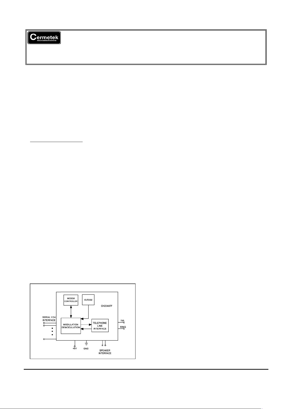
The CH224ATF is a complete FCC Part 68 preapproved, 2400 bps full function modem solution;
incorporating an on-board Data Access
Arrangement (DAA) in a small footprint, socketable packaging format (2.5” L x 1.0 W x 0.45” H).
This product is specifically designed for use as a
direct replacement for Conexant/Rockwell’s
SocketModem (serial TTL I/O option, Part No.
SF224ATF-H1-D5-A0-P1
).
This modem provides a fast and convenient way
to integrate PSTN connectivity into any OEM
product while utilizing a small portion of PCB area.
The CH224ATF requires two external interfaces: a
CCITT V.24 serial interface that is routed directly
from the UART or UART interface, and a TIP and
RING interface, which is connected directly to a
conventional RJ-11 jack for the PSTN line
connection. The CH224ATF also has various
indicator and status lines to monitor operations or
to establish triggers. The CH224ATF modem is
controlled by industry standard “AT” commands
and is compatible with available industry
communication software.
The device supports asynchronous operation at
2400 bps, 1200 bps, and 300 bps to both Bell and
CCIT standards. The resident PSTN line interface
is FCC Part 68 approved, and is also Canadian
DOC approveable, and can be approved in other
countries that require 1500VAC RMS isolation.
Figure 1. Functional Block Diagram of
CH224ATF
FEATURES
• FCC Part 68 pre-approved
• UL1950, 3rd edition listed
• 1500 Vrms isolation
• Complete solution: on-board DAA
• Data modes
- CCITT v.22 bis (2400 bps), V.22 (1200
bps)
- Bell 212A (1200 bps) and 103 (300
bps)
- Enhanced AT commands
• Group 3 fax modes
- V.29 (6900/7200 bps) transmit
- V.27 ter (4800/2400 bps) transmit and
receive
- V.21 Channel 2 (300 bps) transmit
and receive
• EIA-578 Service Class 1 commands
• V.42/MNP2-4 and V.42 bis/MNP5 support
without additional hardware
• Data/fax discriminator and auto answering
• Communications software compatible
• Serial asynchronous DTE interface
• NVRAM interface allows storage of two
user configurations and four 36-digit dial
strings
• Automatic adaptive/fixed compromise
equalization
• Programmable sleep mode
• Full-duplex data mode test capabilities:
Analog loop, local digital loop, and remote
digital loop
• Half-duplex fax mode test capabilities
• Automatic format/speed sensing
• Low power consumption (typical):
Interface Operating Sleep
Serial TTL: 155mW 35mW
• Single +5VDC power supply
TECHNICAL SPECIFICATIONS
General
The CH224ATF modem is a full-featured, selfcontained data/fax solution. External microcontroller for data or fax control functions are
fully supported and controlled through the AT
command set.
2001 Cermetek Microelectronics, Inc. Page 1 Document No. 607-0005 Revision B1 (05/02)
Page 2

Cermetek Microelectronics, Inc. CH224ATF Complete 2400 bps Modem Module
Data modes perform complete handshake and
data rate negotiations. All tone and pattern
detection required by the applicable CCITT or
Bell standard are supported.
Fax modes support Group 3 fax requirements.
Fax data and fax control (V.21 300 bps)
performed by the modem is controlled and
monitored through the fax EIA-578 Class 1
insertion/deletion, and CRC
generation/checking is provided.
Both transmit and receive fax data is buffered
within the modem. Data transfer to and from
the DTE is flow controlled by XON/XOFF.
Configurations and Rates
The supported modem configurations and
signaling rates are listed in Table 1. In data
modes with serial interface selected, DTE rate
offsets of +1%, -2.5% are accommodated by
adding/deleting stop bits are required. In fax
modes, the DTE rate is 19200 bps.
Operation
Modem operation is controlled by AT
commands (Table 2), fax service class 1
commands (Table 3), and supporting S registers
(Table 4). Result codes and messages are
listed in Table 5.
Data Modes: Data rate selection is determined
by the speed of the originating and answering
modems:
Originate Modem Connect Speed Based on
Answer Rate Modem Rate (bps)
(bps)
300 1200 2400
300 300 300 300
1200 1200 1200 1200
2400 1200 1200 2400
Fax Modes: Fax modes are negotiated as
defined in T.30 and are implemented by AT+F
commands. The AT+FCLASS=1 command
causes entry into the fax mode from the data
mode. Most other fax class 1 commands,
which start with the AT+F prefix, are valid only
in the fax mode.All data commands are valid
in the fax mode except A/, On & Tn, and the
escape sequence (+++). The AT+FCLASS=0
command terminates the fax mode and
causes entry into the data mode.
AT Command Format
Each command line must start with the AT
prefix and be terminated with a carriage return
(CR). Several commands may be included on
one command line. A command line may
contain up to 40 characters excluding the AT
prefix and the terminating CR. A separator is
not required between data commands. A
semicolon (;) separator is required between
fax commands.
AT commands are composed of 10-bit ASCII
encoded asynchronous characters. The
character format in data mode is 8 data bits
with no parity, or 7 data bits with even, odd, or
no (two stop bits) parity, at a data rate of
19200, 2400, 1200, or 300 bps. The
character format in fax mode is 8 data bits
with no parity at 19200 bps.
Data Modulation
The data modulation conforms to V.29, V.27
ter, V.22 bis, V.22, V.21, Bell212A, or Bell
103, depending on the selected configuration.
Transmitter and receiver spectrum shaping is
provided in accordance with the applicable
standard.
Equalization
Automatic adaptive qualization as well as
fixed compromised equalization is provided to
compensate for line distortions and to
minimize the effects of the intersymbol
interference.
Scrambler/Descrambler
The modem incorporates a self-synchronizing
scrambler/descrambler satisfying the
applicable CCITT or Bell requirements.
2001 Cermetek Microelectronics, Inc. Page 2 Document No. 607-0005 Revision B1 (05/02)
Page 3
Cermetek Microelectronics, Inc. CH224ATF Complete 2400 bps Modem Module
Table 1. Configurations and Rates
Configurati
on
Modulation Transmitter Carrier
Frequency (Hz) +
0.01%
Data
Rate
(bps)
Baud
(Symbols/
Sec.)
Bits Per
Symbol
Constellation
Points
Data Mode
V.22
V.22
Bell 212A
Bell 103
QAM
DPSK
DPSK
FSK
Answer
2400
2400
2400
2225
2025 S
Originate
1200
1200
1200
1270 M
1070 S
2400
1200
1200
300
600
600
600
300
4
2
2
1
16
4
4
1
Fax Mode
V.29
V.22
Bell 212A
Bell 103
QAM
DPSK
DPSK
FSK
Receive
N/A
N/A
1800
1800
1650 M
1850 S
Transmit
1700
1700
1800
1800
1650 M
1850 S
9600
7200
4800
2400
300
2400
2400
1600
1200
300
4
3
3
2
1
16
8
8
4
1
Notes:
Legend: QAM = Quadrature Amplitude Modulation M = Mark Condition
DPSK = Differential Phase Shift Keying S = Space Condition
FSK = Frequency Shift Keying N/A = Not Applicable
Table 2. “AT” Command Set Summary
Command Function Command Function
A/ Re-execute command &Jn Telephone jack control
A Answer a call &L0 Dial-up line operation
Bn Select CCITT or Bell Mode &M0 Asynchronous mode
Cn Carrier control &Pn Pulse dial make/break ratio
Dn Dial modifier &Q0 Asynchronous mode
En Command echo &Sn DSR override
F1 On-line character echo option &Tn Test and diagnostic
Hn Disconnect (Hangup) &V Display current configurations
In Identification &Wn Store current configuration
Ln Speaker volume &X0 Asynchronous data transmission
Mn Speaker control &Yn Select default profile
On Go on-line &Zn=x Store dial string to location n
P Force pulse dialing %Dn DTMF Level Attenuation
Qn Quiet Result codes control %J Load Secondary Defaults
Sn Select S register as default %Ln Transmit Level Attenuation
Sn=v Set default S register to value Dial Modifier Function
Sn? Return the value of S register P Pulse Dial
T Force DTMF dialing R Originate Call in Answer Mode
Vn Report codes form S=n Dial Stored Number
Xn Extended result codes T Tone Dial
Yn Long space disconnect W Wait for Dial Tone
Zn Soft reset and restore profile ; Return to Idle State
&Cn RLSD (DCD) option @ Wait for Quiet Answer Command
&Dn DTR option ! Flash Hook
&F Recall (restore)factory profile , Pause
&Gn Select guard tone 0-9, A, B, C, D, #, * Dial Digits/ Characters
2001 Cermetek Microelectronics, Inc. Page 3 Document No. 607-0005 Revision B1 (05/02)
Page 4

Cermetek Microelectronics, Inc. CH224ATF Complete 2400 bps Modem Module
Table 3. FAX Command Set Summary Table 4. Register Summary
FAX Command Function
Register Function
+FCLASS=n Service class SO* Rings to Auto –Answer
+F<command>? Report Active Configuration S1 Ring Counter
+F<command>=? Report Operating Capabilities S2 Escape Character
+FAA=n Data/Fax Auto Answer S3 Carriage Return Character
+FF Enhanced flow Control S4 Line Feed Character
+FTS=n Stop Transmissions & Wait S5 Backspace Character
+FRS=n Receive Silence S6 Maximum time to Wait for Dial
Tone
+FTM=n Transmit Data S7 Wait for Carrier
+FRM=n Receive Data S8 Pause Time for Comma
+FTH=n Transmit Data with HDLC
Framing
S9 Carrier Detect Response Time
+FRT=n Receive Data with HDLC
Framing
S10 Carrier Loss Disconnect Time
+FRTn Receive Test Data S11 DTMF dialing Speed
+FTTn=m Transmit Test Data S12 Escape Prompt Delay
+Hn Rockwell Protocol Interface (RPI
Enable)
S14* General Bit mapped Options (&T)
S16 Fax Mode Null Byte Timer
Table 5. Results Codes & Messages
S17 Test Timer
Digit
Code
Word Code Meaning
S18* Rockwell Protocol Interface
Speed
0 OK Command line executed without
errors
S19 Fax ode Inactivity Timer
1 CONNECT Connection at 300bps S20 General bit Mapped Options
2 RING Ringing signal detected S21* General bit Mapped Options
3 NO
CARRIER
Carrier lost or never present S22* General bit Mapped Options
4 ERROR Invalid command, checksum,
error in command line, or
command line exceeds 40
characters
S23* General Bit Mapped Options
5 CONNECT
1200
Connection at 1200 bps S24 Sleep Inactivity Timer
6 NO DIAL
TONE
No dialtone detected S25* Delay to DTR Off
7 BUSY Busy signal detected S26* RTS-to-CTS Delay
8 NO
ANSWER
No silence detected when dialing
a system not providing a dialtone
S27* General Bit Mapped Options
10 CONNECT
2400
Connection at 2400 bps S28* General Bit-Mapped Options
+F4 +FCERROR Fax carrier error * Register value may be stored in one of two user
profiles with the AT&W command.
13 DATA Connected as data modem
during auto answer
15 FAX Connected as fax modem during
auto answer
Data/Fax Auto Answering
The modem can automatically determine if the incoming
call is from a data or fax modem, make the appropriate
connection, and inform the DTE of the connection type.
2001 Cermetek Microelectronics, Inc. Page 4 Document No. 607-0005 Revision B1 (05/02)
Page 5

Cermetek Microelectronics, Inc. CH224ATF Complete 2400 bps Modem Module
Transmit Level
The transmit level is –10 dBm +1
dB (at TIP and
RING).
Answer Tone: An answer tone of 2100 Hz
(V.22bis, V.22, or T.30) or 2225 Hz (Bell 212A
or 103) is generated.
Guard Tone: An 1800 Hz guard tone can be
generated in all data modes.
Calling Tone: A 1100 Hz (0.5 seconds on, 3
seconds on, 3 seconds off) calling tone (T.30) is
generated in the originate fax mode.
Receive Level
The receiver satisfies performance rquirements
for a received signal from –9 dBm to –43 dBm.
The carrier detect is ON at –43 dBm and OFF at
–48 dBm with a minimum of 2 dB hysteresis.
Receiver Tracking
The modem can accommodate carrier
frequency offset up to +
7 Hz, and a transmit
timing error of +
0.01% (V.22 bis or V.27 ter) or
+ 0.02% (V.22 or Bell 212A).
Low Power Sleep Mode
To conserve power, the CH224ATF is
configured for idle (power down) mode. Idle
mode is entered whenever the modem is
inactive beyond the time value specified by S24.
The idle mode allows reduced power
consumption with automatic recovery without
additional circuitry. The modem exits Idle mode
and returns to full operation whenever a ring
signal occurs, the DTE writes to the modem
(parallel interface), or ~DTR or ~TXD is asserted
(serial interface).
HARDWARE INTERFACE
Serial/Indicator Interfaces
A DTE serial interface and indicator output are
supported.
Serial Interface. A TTL logic serial interface to
the DTE is supported.
LED indicator interface. Four direct connect
LED indicator outputs are supported.
Speaker Interface
A speaker output, controlled by AT or V.25 bis
commands, is provided for an optional OEMsupplied speaker circuit.
Line Interface
The CH224ATF connects to the telco line via tip
and ring signals.
LOW POWER MODES
Sleep mode
Entry. The modem will enter the low power
sleep mode when no line connection exists and
no host activity occurs for the period of time
specified in the S24 register. All device circuits
are turned off except the internal MCU clock
circuitry in order to consume lower power, but
are able to immediately wake up and resume
normal operation.
Wake-up. Wake-up occurs when a ring signal
occurs, or the DTE sends a character to the
modem.
HARDWARE INTERFACE SIGNALS
The SocketModem pin assignments for serial
TTL interface selected are shown in Figure 2
and are listed in Table 7.
The SocketModem hardware interface signals
are defined in Table 9.
The digital electrical characteristics for the
hardware interface signals are listed in Table
10.
The analog electrical characteristics for the
hardware interface signals are listed in Table
11.
The current absolute maximum ratings are listed
in Table 13.
2001 Cermetek Microelectronics, Inc. Page 5 Document No. 607-0005 Revision B1 (05/02)
Page 6

Cermetek Microelectronics, Inc. CH224ATF Complete 2400 bps Modem Module
Figure 3. CH224ATF (Serial TTL Pinout)
~DCDTTL
~CTSTTL
DAA
25NC
33
34
35
36
37
38
39
40
41
61
62
63
64
32
31
30
29
27
26
24
2
1
NC
~R
X
DTTL
~TXDTTL
~RITTL
~DSRTTL
~DTRTTL
DGND
TXIND
~DTRIND
RXIND
DCDIND
NC
DGND
~RESET
VCC
NC
A
GND
SPKR
RING
TIP
2001 Cermetek Microelectronics, Inc. Page 6 Document No. 607-0005 Revision B1 (05/02)
Page 7

Cermetek Microelectronics, Inc. CH224ATF Complete 2400 bps Modem Module
Table 7. CH224ATF Serial TTL Signals
Pin Signal I/O Type Pin Signal I/O Type
1
2
3
4
5
6
7
8
9
10
11
12
13
14
15
16
17
18
19
20
21
22
23
24
25
26
27
28
29
30
31
32
TIP
RING
NO PIN
NO PIN
NO PIN
NO PIN
NO PIN
NO PIN
NO PIN
NO PIN
NO PIN
NO PIN
NO PIN
NO PIN
NO PIN
NO PIN
NO PIN
NO PIN
NO PIN
NO PIN
NO PIN
NO PIN
NO PIN
~RESET
N0 PIN
DGROUND
NC
NO PIN*
DCDIND
RXIND
DTRIND
TXIND
IF
IF
-
-
-
-
-
-
-
-
-
-
-
-
-
-
-
-
-
-
-
-
-
IC
-
GND
-
-
OG
OG
OG
OG
33
34
35
36
37
38
39
40
41
42
43
44
45
46
47
48
49
50
51
52
53
54
55
56
57
58
59
60
61
62
63
64
NC
~RXDTTL
~TXDTTL
~RITTL
~DSRTTL
~CTSTTL
~DCDTTL
~DTRTTL
DGROUND
NO PIN
NO PIN
NO PIN
NO PIN
NO PIN
NO PIN
NO PIN
NO PIN
NO PIN
NO PIN
NO PIN
NO PIN
NO PIN*
NO PIN*
NO PIN*
NO PIN*
NO PIN*
NO PIN*
NO PIN*
VCC
NC
AGROUND
SPKR
-
OA
IA
OA
OA
OA
OA
IA
GND
-
-
-
-
-
-
-
-
-
-
-
-
-
-
-
-
-
-
-
PWR
-
GND
O(DF)
* It is suggested that a hole be placed in the host board for upgrade purposes.
2001 Cermetek Microelectronics, Inc. Page 7 Document No. 607-0005 Revision B1 (05/02)
Page 8

Cermetek Microelectronics, Inc. CH224ATF Complete 2400 bps Modem Module
Table 9. Signal Designations
Label I/O Signal Name Designation
The Serial Interface signals are all TTL-level.
~RXDTTL OA Received Data. Active low. The modem uses the ~RXD line to send data
received from the telephone line to the DTE and to send modem responses to the
DTE. During command mode, ~RXD data represents the modem responses to
the DTE. Modem responses take priority over incoming data when the two
signals are in competition for ~RXD.
~TXDTTL IA Transmitted Data. Active low. The DTE uses the ~TXD line to send data to the
modem for transmission over the telephone line or to transmit commands to the
modem. The DTE should hold this circuit in the mark state when no data is being
transmitted or during intervals between characters.
~RITTL OA Ring Indicate. Active low. ~RI output ON (low) indicates the presence of an ON
segment of a ring signal on the telephone line. The modem will not go off-hook
when ~RI is active; the modem waits for ~RI to go inactive before going off-hook.
For US models, ~RI will respond to ring signals in the frequency range of 15.3 Hz
to 68 Hz. The ring signal cycle is typically two seconds ON, four seconds OFF.
The OFF (high) condition of the ~RI input should be maintained during the OFF
segment of the ring cycle (between rings) and at all other times when ringing is
not being received.
~DSRTTL OA Data Set Ready. Active low. ~DSR indicates modem status to the DTE. ~DSR
OFF (high) indicates that the DTE is to disregard all signals appearing on the
interchange circuits except Ring indicator (~RI). ~DSR output is controlled by the
AT&Sn command.
If the AT&S1 option is selected, ~DSR will come ON in the handshaking state
when carrier is detected in the originate mode or when carrier is first sent in the
answer mode. In addition if a test mode is entered (AT&T1, AT&T3, AT&T6AT&T8), ~DSR will go off while the test is running. ~DSR goes OFF if ~DTR goes
OFF.
If AT&Q0 and AT&S0 are selected, ~DSR will remain on at all times regardless of
the modem’s current state.
~CTSTTL OA Clear To Send. Active low. ~CTS is controlled by the modem to indicate
whether or not the modem is ready to transmit data. CTS OFF indicates to the
DTE that it should not transfer data across the interface on TXD. In data modes,
the ~CTS output is always ON. In fax modes, ~CTS is optionally used for flow
control.
~DCDTTL OA Data Carrier Detect. Active low. When AT&C0 commands is not in effect, ~DCD
output is ON when a carrier is detected on the telephone line or OFF when carrier
is not detected.
~DCD can be strapped ON using AT&C0 command.
~DTRTTL IA Data Terminal Ready. Active low. The ~DTR input is turned ON (low) by the
DTE when the DTE is ready to transmit or receive data. ~DTR ON prepares the
modem to be connected to the telephone line, and maintains the connection
established by the DTE (manual answering) or internally (automatic answering).
~DTR OFF places the modem in the disconnect state under control of the &DN
and &Qn commands. The effect of ~DTR ON and ~DTR OFF depends on the
&Dn and &Qn commands. Automatic answer is enabled when ~DTR is ON if the
“Answer Ring count” selectable option is not set to 0. Regardless of which device
is driving ~DTR, the modem will respond to an incoming ring by going off-hook
and beginning the handshake sequence.
The response of the modem to the ~DTR signal is very slow (up to 10 ms) to
prevent noise from falsely causing the modem to disconnect from the telephone
line.
2001 Cermetek Microelectronics, Inc. Page 8 Document No. 607-0005 Revision B1 (05/02)
Page 9

Cermetek Microelectronics, Inc. CH224ATF Complete 2400 bps Modem Module
Table 9. Signal Designations (Continuation).
GND GND
Ground
LED drivers are open-drain inverter-driven (74HCT05) lines with 1.5K ½,
1/10W pull-up resistors on-board.
DCDIND OG DCD LED indicator. Active high DCD status.
RXIND OG RXD LED indicator. Active high RXD status.
DTRIND OG DTR LED indicator. Active high DTR status.
SPKR O(DF) Speaker Analog Output. The SPKR output reflects the received analog input
signal. The SPKR is controlled by the ATMn command.
SKR is tied directly to SPKR pin of the data pump.
TXIND OG TXD LED indicator. Active high TXD status.
Table 10. Digital Interface Characteristics
Parameter Symbol Min. Typ. Max. Units Test Conditions
Input High Voltage
Type IA
Type IC
Type IH
V
IH
2.0
3.5
-30
-
-
-
V
CC
V
CC
30
Vdc
Input Low Voltage
Type IA and IC
VIL
-0.3
-
0.8
Vdc
Input Low Voltage
Type IF
VIL
38
-
-
Vrms
Note 2
Input Leakage Current
IA and IC
IIN -
-
+10
µAdc
VIN=0 to VCC
Output High Voltage
Type OA
Type OD
Type OG
V
OH
2.4
-
-
-
-
-
-
V
CC
VCC
Vdc
I
LOAD
= 100µA
I
LOAD
= 0 mA
I
LOAD
= 0 mA
Output Low Voltage
Type OA
Type OB
Type OD
Type OG
V
OL
Vdc
I
LOAD
= 1.6 mA
I
LOAD
= 0.8 mA
I
LOAD
= 15 mA
I
LOAD
= 8 mA
Three –State (Off)
Current
ITS +25
µAdc
VIN=0.8 V to 4.5V
Notes:
1. Test Conditions: V
CC
= 5V + 5%, TA = 0°C to 70°C (unless otherwise stated.)
Output loads: 50 pF + one TTL.
2. AC Vrms voltage between Tip and Ring, using the on-boatd modular DAA.
Table 11. Analog Characteristics
Name Type Characteristic Value
SPKR O (DF) Minimum Load
Maximum Capacitive
Load
Output Impedance
Output Voltage
D.C Offset
300Ω
0.01µF
10Ω
2.5 +
1.6V
< 20 mV
2001 Cermetek Microelectronics, Inc. Page 9 Document No. 607-0005 Revision B1 (05/02)
Page 10

Cermetek Microelectronics, Inc. CH224ATF Complete 2400 bps Modem Module
Table 12. Current and Power Requirements
Current (ID) Power (PD)
Mode
Typical
Current
@25°C
Maximum
Current
@0°C
Typical
Power
@25°C
Maximum Power
@0°C
Serial TTL
Normal mode
Sleep mode
31mA
7 mA
33 mA
9 mA
155 mW
35 mW
165 mW
45 mW
Notes:
1. Test conditions: 5.0 VDC for typical values; VDD = 5.25 for maximum values.
Table 13. Absolute Maximum Ratings
Parameter Symbol Limits Units
Supply Voltage VDD -0.5 to +6.0 V
Input Voltage VIN -0.5 to (+5VD +0.5) V
Analog Inputs VIN -0.3 to (+5VA +0.3) V
Voltage Applied to Outputs in High Z State VDD -0.5 to (+5VD +0.5) V
DC Input Clam Current IIK +20 MA
DC Output Clamp Current IOK +20 MA
Static Discharge Voltage (@25°C)
V
ESD
+2500 V
Latch-Up Current (@25°C)
I
TRIG
+400 mA
Operating Temperature Range TA -0 to +70
°C
Storage Temperature Range T
STG
-40 to +80
°C
PHONE LINE CONNECTION GUIDELINES
1. The CH224ATF must be mounted in the
final assembly such that it is isolated from
exposure to any hazardous voltages within
the assembly. Adequate separation and
restraint of cables and cords must be
provided.
2. The circuitry from the CH224ATF to the
telephone line interface must be provided
in wiring that carries no other circuitry
other than that specifically allowed in the
FCC rules (such as A and A1 leads).
3. Connection to phone line should be made
through an RJ-11C jack.
4. PCB traces from the modem’s RING and
TIP pins to the RJ-11C jack must be 0.1
inch spacing or greater to one another and
0.2 inch spacing or greater to all other
traces. The traces should have a nominal
width of 0.020 inches or greater.
5. The RING and TIP PCB traces should be
as short as possible and oriented to
prevent coupling other high speed or high
frequency signals present on the host
circuit PCB.
6. No additional circuitry other than that
shown in Figure 7A or 7B may be
connected between the modem module
and the RJ-11C jack. Doing so will
invalidate the FCC approval.
7. The CH224ATF requires external surge
protection (see Figure 7). This is mandatory
to maintain FCC Part 68 conveyed approval.
8. The CH224ATF, the RJ-11C jack, the
interfacing circuitry and all PCB traces in
between, must be contained on a PCB with a
94 V-0 flammability rating.
9. The supplied FCC registration label must be
applied visibly on the outside of the product.
10. The product ’s User Manual must provide the
user with instructions for connection and use
as recommended in the FCC Registration
Section below.
FCC REGISTRATION
All products in the CH224ATF series are
registered with the FCC (Federal
Communications Commission) under Part 68. To
maintain the validity of the registration, you must
serve notice to the end user of the product of
several restrictions the FCC places on the
modem and its use.
The CH224ATF requires external surge
protection (see Figure 7). This is mandatory to
maintain FCC Part 68 conveyed approval. Refer
to Cermetek Application Note #126 for more
details.
2001 Cermetek Microelectronics, Inc. Page 10 Document No. 607-0005 Revision B1 (05/02)
Page 11

Cermetek Microelectronics, Inc. CH224ATF Complete 2400 bps Modem Module
In addition to restriction notification, the FCC
requires that Cermetek make all repairs to all
products in the CH224ATF. If repairs are
necessary after installation of the CH224ATF in
the end product and the end product has been
delivered to the end user, the end product must
be returned to the end product supplier where
the CH224ATF can be removed and then
forwarded to Cermetek for repair. The
following notice is recommended and should
be included in the end product ’s user manual.
INTERNATIONAL APPROVALS
The CH224ATF can be approved for some
international telephone connections. This must
be done after the modem is installed in the host
product.
The entire host product must be submitted to
the country of interest’s Telephone Network
approval authority. The end product supplier is
responsible for submission of the end product
for independent testing and subsequent
approval. See Application Cermetek Note
#142 for typical telephone requirements.
CH224ATF HANDLING AND ASSEMBLY
RECOMMENDATIONS
The CH224ATF contains static-sensitive
compo-nents and should only be handled by
personnel and in areas that are properly
protected against static discharge.
FOR YOUR USER ’S MANUAL
The Part 68 rules require the following (or
equivalent) be provided to the end user of
equipment containing a DAA:
Type of Service: The (insert end product
name)is designed to be used on standard
device telephone lines. It connects to the
telephone line by means of a standard jack
called the USOC RJ-11C (or USOC RJ45S).
Connection to telephone-company-pro-vided
coin service (central office implemented
systems) is pro-hibited. Connection to party
lines service is subject to state tariffs.
Changes in Attestation Procedure for Plugs
and Jacks: (Name of applicant) attests that the
network interface plugs or jacks used on this
equipment comply with and will continue to
comply with the mechanical requirements
specified in Part 68, Sub-part F, specifically the
dimensions, tolerances and metallic plating
requirements. The compliance of these
connectors will be assured by purchase
specifications and incoming inspection.
Documentation of such specifications and/or
inspections will be provided to the FCC within 30
days of their request for the same.
Telephone Company Procedures: The goal of
the telephone company is to provide you with the
best service it can. In order to do this, it may
occasionally be necessary for them to make
changes in their equipment, operations or
procedures. If these changes might affect your
service or the operation of your equipment, the
telephone company will give you notice, in writing,
to allow you to make any changes necessary to
maintain uninterrupted service.
In certain circumstances, it may be necessary for
the telephone company to request information
from you concerning the equipment which you
have connected to your telephone line. Upon
request of the telephone company, provide the
FCC registration number and the ringer
equivalence number (REN); both of these items
are listed on the equipment label. The sum of all
of the REN ’s on your telephone lines should be
less than five in order to assure proper service
from the telephone company. In some cases, a
sum of five may not be useable on a given line.
Consult your telephone provider.
If Problems Arise: If any of your telephone
equipment is not operating properly, you should
immediately remove it from your telephone line,
as it may cause harm to the telephone network. If
the telephone company notes a problem, they
may temporarily discontinue service. When
practical, they will notify you in advance of this
disconnection. If advance notice is not feasible,
you will be notified as soon as possible.
2001 Cermetek Microelectronics, Inc. Page 11 Document No. 607-0005 Revision B1 (05/02)
Page 12

Cermetek Microelectronics, Inc. CH224ATF Complete 2400 bps Modem Module
1. Current Limiting PSTN Protection Line
Device.
Current limiting is mandatory to meet UL safety
requirements. To maintain conveyed FCC Part
68 approval, the current limiting devices
identified as F1and F2 in dashed box #1 must
also survive FCC Part 68 surge tests. Use one
of the external component schemes defined
below in section 1A-1C to maintain compliance.
Reference Cermetek Application Note #126,
Supplemental PSTN Line Protection, for a more
detailed discussion.
A. A Raychem Polyfuse TR 600-150 (rated at 0.15
amps) is preferred because this device resets
automatically upon removal of the current flow.
Non-resettable devices such as Littlefuse, type
220003, or WICKMANN 19397-038 are also
acceptable.
B. Resistors (10Ω carbon film or 1/8 watt
minimum) may be used in Canada, as Canada
has no requirement that PSTN equipment be
operational after a type B surge test.
C. Although CSA CS-03 Part 1 (Canada) follows
the requirements of FCC Part 68 (USA),
Cermetek recommends contacting DOT
(Canada) and/or a certified independent lab to
verify compliance. For Canada, use either 10Ω
resistors (carbon film or SMD parts 1/8 watt
minimum) as described in paragraph B above,
or non-resettable fuses or resettable Polyfuses
as described in paragraph A above.
2. Over Voltage and Lightning Protection.
Surge Protection must be provided by
additional external components. This is
required to maintain conveyed FCC Part 68
approval. Refer to Cermetek Application Note
#126, Supplemental PSTN Line Protection, for
a more detailed discussion.
3. EMI/RFI Suppression.
No external EMI/RFI noise suppression circuitry
is required to maintain conveyed FCC Part 68
approval. However additional suppression, if
required for other reasons, may be added as
described below in Sections 3A–3B without
adversely effecting the FCC Part 68 approval.
A. To provide adequate EMI/RFI suppression, the
capacitor/inductor network contained in dashed
Box #3, Figure 1, should be located as close to
the RJ11 Jack as possible. Further, this
network should be provided with an excellent
ground path to the chassis.
B. Capacitors C1 and C2 should not exceed 0.005
µf. They must have a rating of 1.5 KV and
typically are .001 µf ± 20%. Recommended
devices for inductors L1 and L2 are Fair-Rite
2643666611 or 2943666661 or equivalent. For
UL applications, choose capacitors and
inductors that are UL 1950 listed. The actual
values of the components used may vary
depending on the end product design.
2001 Cermetek Microelectronics, Inc. Page 12 Document No. 607-0005 Revision B1 (05/02)
Page 13

Cermetek Microelectronics, Inc. CH224ATF Complete 2400 bps Modem Module
2001 Cermetek Microelectronics, Inc. Page 13 Document No. 607-0005 Revision B1 (05/02)
Table 14. CH224ATF Family of Products
Model Summary of Features Operating Temperature
CH224ATF Full Function, FCC Part 68 Approved, UL1950 Listed,Non-Hermetic
0°C to 70°C
Figure 5. CH224ATF Physical Dimensions
Cermetek reserves the right to make changes in specifications at any time and without notice. The information furnished by
Cermetek in this publication is believed to be accurate and reliable. However, no responsibility is assumed by Cermetek for its
use, or for any infringements of patents or other rights of third parties resulting from its use. No license is granted under any
patents or patent rights of Cermetek.
Printed in U.S.A
406 TASMAN DRIVE | SUNNYVALE CA 94089 | LOCAL: 408-752-5000 | TOLL FREE: 1-800-882-6271
FAX: 408-752-5004 | WEB SITE: http://www.cermetek.com
| EMAIL: sales@cermetek.com
 Loading...