

Page 1
September 1995
Revised March 1999
CGS3311 • CGS3312 • CGS3313 • CGS3314 • CGS3315 • CGS3316 • CGS3317 • CGS3318 • CGS3319 CMOS Crystal
Clock Generators
© 1999 Fairchild Semiconductor Corporation DS010980.prf www.fairchildsemi.com
CGS3311 • CGS3312 • CGS3313 • CGS3314 • CGS3315 •
CGS3316 • CGS3317 • CGS3318 • CGS3319
CMOS Crystal Clock Generators
General Description
The CGS3311, CGS3312, CGS3313, CGS3314,
CGS3315, CGS3316 , CGS 3317, CGS33 18 an d CGS33 19
devices are designed for Clock Generation and Support
(CGS) applications up to 110 MHz. The CGS331x series of
devices are crystal controlled CMOS oscillators requiring a
minimum of external components. The 331x devices provide selectable output divide ratio (a nd selectable crystal
drive level). The ci rcuit is designed to operat e over a wide
frequency range using fundamental model or overtone
crystals.
Features
■ Fairchild’s CGS family of devices for high frequency
clock source applications
■ Crystal frequency operation range:
fundamental: 10 MHz to 100 MHz typical
3rd or 5th overtone: 10 MHz to 85 MHz
■ Programmable oscillator drive
■ Selectable fast output edge rates
■ Output symmetry circuit to adjust 50% duty cycle point
between CMOS and TTL levels
■ Output current drive of 48 mA for I
OL/IOH
■ FACT CMOS output levels
■ Output has high speed short circuit protection
■ Basic oscillator type: Pierce
■ Hysteresis inputs to improve noise margin
Ordering Code:
Devices also availab le in Tape and Reel. Specify by appending th e s uffix let t er “X” to the ordering cod e.
FACT is a trade m ark of F airchild Semicondu ctor Corporation.
Order Number Package Number Package Description
CGS3311M M08A 8-Lead Small Outline Integrated Circuit (SOIC), JEDEC MS-012, 0.150” Narrow Body
CGS3312M M08A 8-Lead Small Outline Integrated Circuit (SOIC), JEDEC MS-012, 0.150” Narrow Body
CGS3313M M08A 8-Lead Small Outline Integrated Circuit (SOIC), JEDEC MS-012, 0.150” Narrow Body
CGS3314M M08A 8-Lead Small Outline Integrated Circuit (SOIC), JEDEC MS-012, 0.150” Narrow Body
CGS3315M M08A 8-Lead Small Outline Integrated Circuit (SOIC), JEDEC MS-012, 0.150” Narrow Body
CGS3316M M08A 8-Lead Small Outline Integrated Circuit (SOIC), JEDEC MS-012, 0.150” Narrow Body
CGS3317M M08A 8-Lead Small Outline Integrated Circuit (SOIC), JEDEC MS-012, 0.150” Narrow Body
CGS3318M M08A 8-Lead Small Outline Integrated Circuit (SOIC), JEDEC MS-012, 0.150” Narrow Body
CGS3319M M08A 8-Lead Small Outline Integrated Circuit (SOIC), JEDEC MS-012, 0.150” Narrow Body
Page 2
www.fairchildsemi.com 2
CGS3311 • CGS3312 • CGS3313 • CGS3314 • CGS3315 • CGS3316 • CGS3317 • CGS3318 • CGS3319
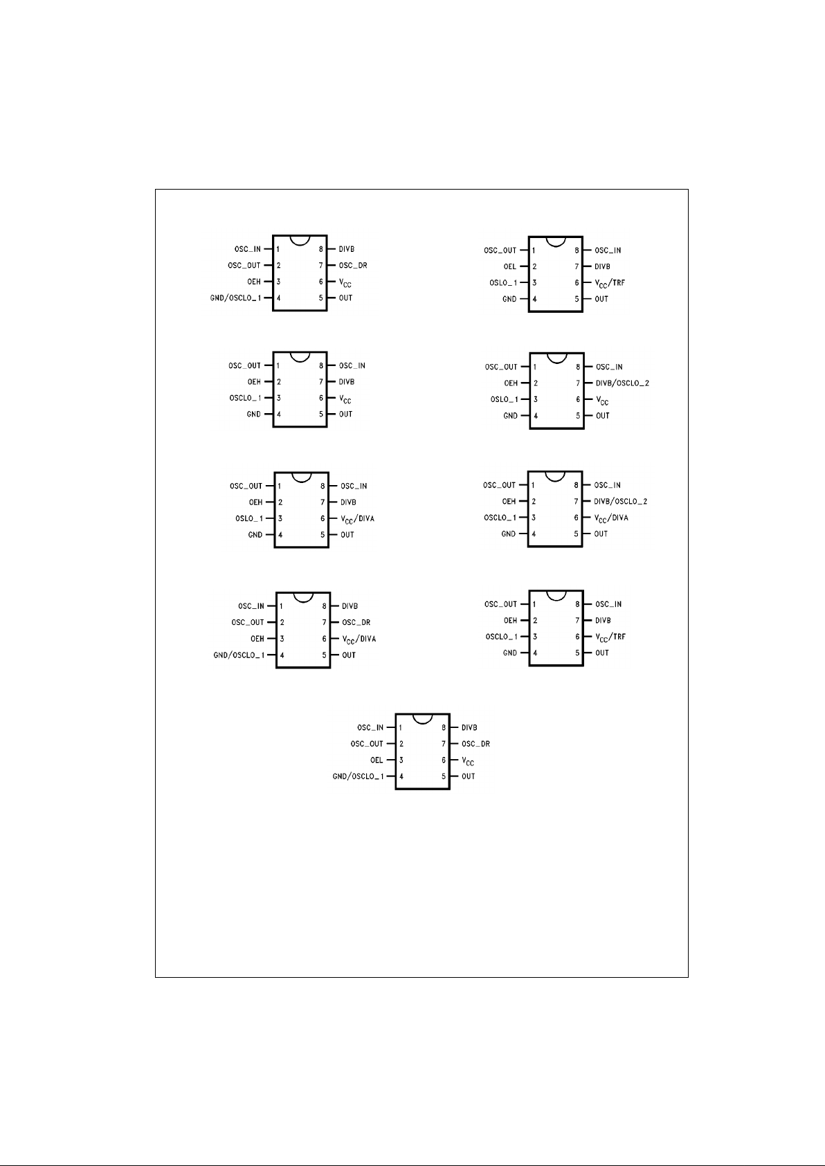
Connection Diagrams
(A) 3311
(B)3312
(C) 3313
(D) 3314
(E) 3315
(F) 3316
(G) 3317
(H) 3318
(I) 3319
Page 3
3 www.fairchildsemi.com
CGS3311 • CGS3312 • CGS3313 • CGS3314 • CGS3315 • CGS3316 • CGS3317 • CGS3318 • CGS3319
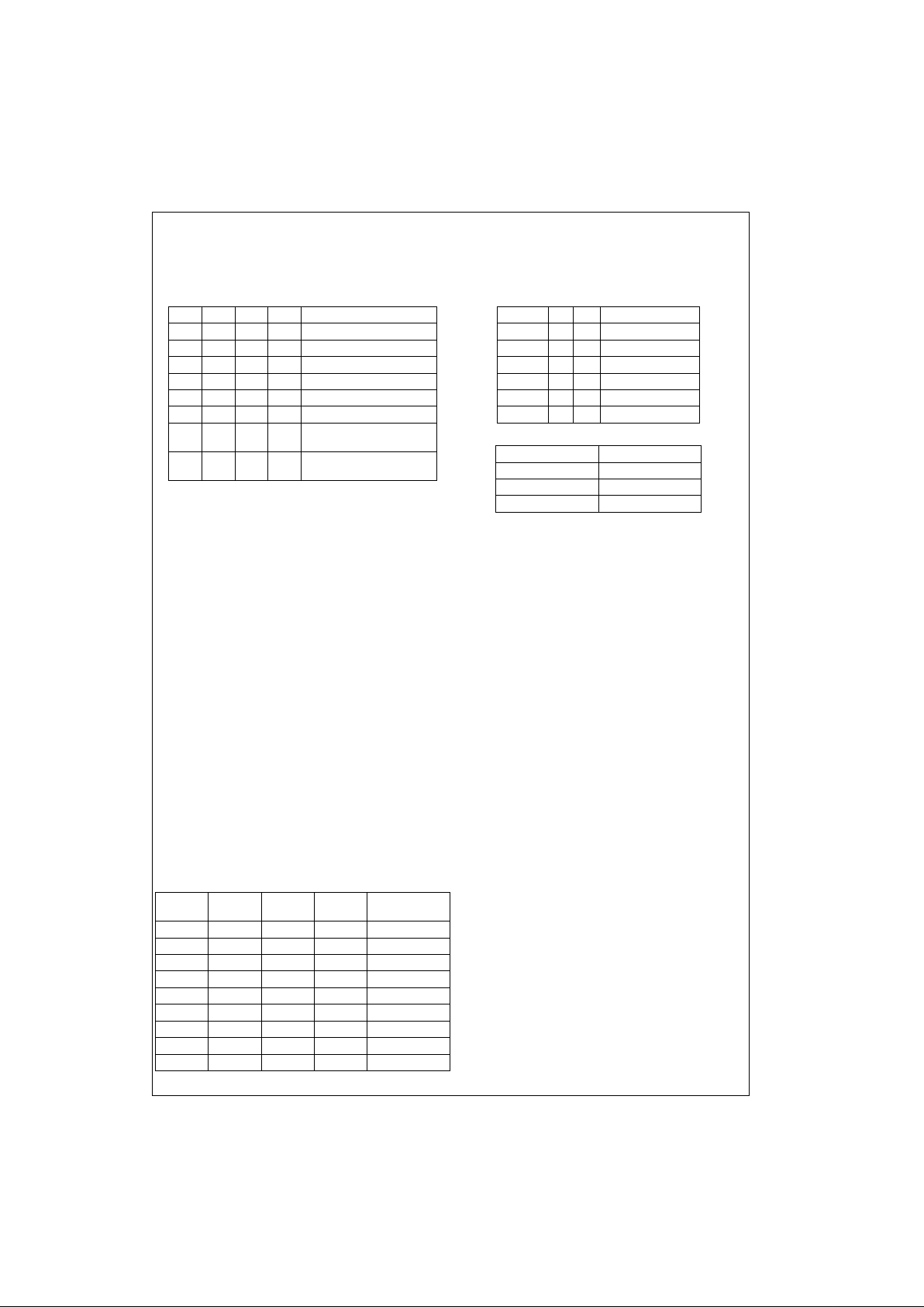
Truth Tables
Division Selection
Note: Actual value of the fl oat ing OSC_DR and DIV B input is V
CC/2
Rise and Fall Time Selection
Drive Selection
Note: Where “F” indicates floating the input.
Pin Descriptions
Functional Table
Summary of Device Options
Each drive has one output with the choices of selecting frequency divide,
output enable, c rystal drive and output rise and fall time. Crystal drive
options are:
L = LOW Drive
M = MEDIUM Drive
H = HIGH Drive
DIVB DIVA OEL OEH Divider Output
F 0/F X X Divide-by 1
1 0/F 0 1 Divide-by 2
0 0/F 0 1 Divide-by 4
F 1 0 1 Divide-by 8
1 1 0 1 Divide-by 16
0 1 0 1 Divide-by 32
X X 1 X Output Reset HIGH
at Re-enable
X X X 0 Output Reset HIGH
at Re-enable
OSC_DR DIV TRF Rise/Fall Time (ns)
FN0/F2
F N 1 less than 2
FY0/F4
FY12
0,1 X 0/F 4
0,1 X 1 2
OSC_DR Drive
0Low
1 Medium
F High
Note: Pin out varies for each device.
OSC_IN Input to Oscillator Inverter. The output of the
crystal would be connected here.
OEL Active LOW 3-STATE enable pin. This pin pulls
to a low value when left floating and 3-STATE
the output when forced HIGH. This pin has TTL
compatible input levels.
OSC_OUT Resistive Buffered Output of the Oscillator
Inverter
TRF Rise and Fall time override pin. Available only
for die form.
OSC_DR 3 Level input pin that selects Oscillator Drive
Level
OUT This pin is the main clock output on the device.
DIVA Input used to select Binary Divide-by Option.
This pin has CMOS compatible input levels.
OSCLO_1 The Oscillator LOW pin is the ground for the
Oscillator.
OEH Active HIGH 3-STATE enable pin. This pin pulls
to a high value when left floating and 3-STATEs
the output when forced low. This pin has TTL
compatible input levels.
OSCLO_2 This pin is the same signal as OSCLO_1. It has
been provided as an alternate connection for
OSCLO_1 for hybrid assemblies.
V
CC
The power pin for the chip.
GND The ground pin for all sections of the circuitry
except the oscillator and oscillator related
circuitry.
Device Divide Enable Drive
Output Rise/
Fall Time (ns)
3311 1, 2, 4 OEH L, M, H 2, 4
3312 1, 2, 4 OEH H 2, 4
3313 8, 16, 32 O E H H 4
3314 8, 16, 32 O E H L, M, H 4
3315 1, 2, 4 OEL H 1, 2
3316 4 OEH H 4
3317 32 OEH H 4
3318 1, 2, 4 OEH H 1, 2
3319 1, 2, 4 OEL L, M, H 2, 4
Page 4

www.fairchildsemi.com 4
CGS3311 • CGS3312 • CGS3313 • CGS3314 • CGS3315 • CGS3316 • CGS3317 • CGS3318 • CGS3319
Block Diagrams
Note: Pin numbers vary for each device
Oscillator Stage
Output Stage
Page 5

5 www.fairchildsemi.com
CGS3311 • CGS3312 • CGS3313 • CGS3314 • CGS3315 • CGS3316 • CGS3317 • CGS3318 • CGS3319
Absolute Maximum Ratings(Note 1) Recommended Operating
Conditions
Note 1: The Absolute Maximum Ratings are those values beyond which
the safety of the device cannot be guaranteed. The device should not be
operated at these limit s. The paramet ric values de fined in the DC and AC
Electrical Characteristics tables are not guaranteed at the absolute maximum ratings. The R ec ommended Operating Conditions w ill define the conditions for actual dev ic e operation.
DC Electrical Characteristics
Supply Voltage (VCC) −0.5V to 7.0V
DC Input Voltage Diode Current (I
IK
) ±9 mA
DC Input Voltage (V
I
) −0.5V to 7.0V
DC Output Diode Current (I
OK
) ±20 mA
DC Output Voltage (V
O
) -0.5V to VCC + 0.5V
DC Output Source
or Sink Current (I
O
) ±70 mA
Storage Temperature ( T
STG
) −55°C to 150°C
Junction Temperature (T
J
)
SOIC 140°C/W
Supply Voltage (V
CC
) 4.5V to 5.5V
Input Voltage (V
I
)0V to 5.5V
Output Voltage (V
O
)0V to V
CC
V
Operating Temperature (T
A
) −40° to +85°C
Symbol Parameter
TA = +25°CT
A
= −40° C to +85°C
Units Conditions
V
CC
Typ
Guaranteed Limits
(V) Min Max Min Max
V
IHTTL
Minimum HIGH Level
Input Voltage,
TTL Level Inputs (OEH, OEL)
4.5 2.0 2.0 V
5.5 2.0 2.0
V
ILTTL
Maximum LOW Level
Input Voltage, TTL Level
Inputs (OEH, OEL)
4.5 0.8 0.8 V
5.5 0.8 0.8
V
IHCMOS
Minimum HIGH Level
Input Voltage. CMOS
Level Inputs (DIVA)
4.5 3.15 3.15 V
5.5 3.85 3.85
V
ILCMOS
Maximum LOW Level
Input voltage. CMOS
Level Inputs (DIVA)
4.5 1.35 1.35 V
5.5 1.65 1.65
V
IN3L_H
Minimum Logic 1 Input
for Three Level Input
(DIVB, OSC_DR)
4.5 4.05 4.05 V
5.5 4.95 4.95
V
IN3L_1/2
Minimum Logic 1/2 Input
for Three Level Input
(DIVB, OSC_DR)
4.5 1.8 2.7 1.8 2.7 V
5.5 2.2 3.3 2.2 3.3
V
IN3L_L
Maximum Logic 0 Input
Level Three Level Input
(DIVB, OSC_DR)
4.5 0.45 0.45 V
5.5 0.45 0.45
V
OH
Minimum HIGH Level
Output Voltage
4.5 4.49 4.40 4.40 V I
OUT
= −50µA
5.5 5.49 5.40 5.40
4.5 3.86 3.76 IOH = −48 mA
5.5 4.86 4.76 VIN = VIH or V
IH
V
OL
Minimum LOW Level
Output Voltage
4.5 0.001 0.1 0.1 V I
OUT
= 50µA
5.5 0.001 0.1 0.1
4.5 0.44 0.44 IOL = +48mA
5.5 0.44 0.44 VIN = VIL or V
IH
I
IHRES
Input Current for Pins
DIVB, OSC_DR, and
DIVA (Input is Logic HIGH)
5.5 220 360 200 380 µAVIN = 5.5V
I
ILRES
Input Current for Pins
DIVB, OSC_DR, and
DIVA (Input is Logic LOW)
5.5 −220 −360 −200 −380 µAVIN = 0.0V
I
IHENAB
Input Current for
Enable Pin OEL
5.5 90 160 85 175 µAVIN = 5.5V
I
ILENAB
Input Current for
Enable Pin OEH
5.5 −90 −160 −85 −175 µAVIN = 0.0V
I
IHOSC
Input Current for OSC_IN Pin
(Indicates Bias Resistance)
5.5 20 100 20 125 µAV
IN
= 5.5V
I
ILOSC
Input Current for OSC_IN Pin
(Indicates Bias Resistance)
5.5 −20 −100 −20 −125 µAVIN = 0.0V
I
OZH
Output Disabled Current 4.5 3.0 5.0 µAV
OUT
= V
CC
(Output HIGH) 5.5 3.0 5.0
Page 6

www.fairchildsemi.com 6
CGS3311 • CGS3312 • CGS3313 • CGS3314 • CGS3315 • CGS3316 • CGS3317 • CGS3318 • CGS3319
DC Electrical Characteristics (Continued)
AC Electrical Characteristics
Over recommended operating free air temperature range. All typical values are measured at V
CC
= 5V, T
A
= 25°C.
Note 2: Voltage Range 5.0 is 5. 0V ± 0.5V
Symbol Parameter
TA = +25°CT
A
= −40° C to +85°C
Units Conditions
V
CC
Typ
Guaranteed Limits
(V) Min Max Min Max
I
OZL
Output Disabled Current 4.5 −140 −150 µAV
OUT
= 0.0V
(Output LOW) 5.5 −170 −180
I
OLD
Minimum Dynamic
Output Current
5.5 75 75 mA V
OLD
= 1.65v
I
OHD
Minimum Dynamic
Output Current
5.5 −75 −75 mA V
OHD
= 3.85V
I
CCOSC_L
Additional ICC with OSC_IN 4.5 0.6 0.6 mA OSC_IN = Float
Floating. LOW Drive Mode 5.5 6.5 6.5
I
CCOSC_M
Additional ICC with OSC_IN 4.5 1.7 1.7 mA OSC_IN = Float
Floating. LOW Drive Mode 5.5 12.4 12.4
I
CCOSC_H
Additional ICC with OSC_IN 4.5 5.5 5.5 mA OSC_IN = Float
Floating. LOW Drive Mode 5.5 31.5 31.5
I
CCT
Additional Maximum ICC
per Input
(OEH, OEL Pins)
5.5 1.5 1.5 mA VIN = VCC − 2.1V
I
CC3L
Additional Maximum ICC
per Input
(DIVB, OSC_DR Inputs)
5.5 1.5 1.5 mA DIVB, OSC_DR
Inputs Equal to V
CC/2
Symbol Parameter
V
CC
TA = −40°C to + 85°C
Units
(V)
CL = 50 pF
(Note 2) Min Type Max
f
MAX
Frequency Maximum 5.0 100 ns
t
PZH
Output HIGH Enable Time 5.0 1.0 31.5 ns
t
PZL
Output LOW Enable Time 5.0 1.0 28.0 ns
t
PHZ
Output HIGH Disable Time 5.0 1.0 21.5 ns
t
PLZ
Output LOW Disable Time 5.0 1.0 16.0 ns
t
RISE
Rise/Fall Time 5.0 4.0 ns
t
FALL
30 pF (20% to 80%)
Page 7

Fairchild does not assume any responsibility for use of any circuitry described, no circuit patent licenses are implied and Fairchild reserves the right at any time without notice to change said circuitry and specifications.
CGS3311 • CGS3312 • CGS3313 • CGS3314 • CGS3315 • CGS3316 • CGS3317 • CGS3318 • CGS3319 CMOS Crystal
Clock Generators
LIFE SUPPORT POLICY
FAIRCHILD’S PRODUCTS ARE NOT AUTHORIZED FOR USE AS CRITICAL COMPONENTS IN LIFE SUPPORT
DEVICES OR SYSTEMS WITHOUT THE EXPRESS WRITTEN APPROVAL OF THE PRESIDENT OF FAIRCHILD
SEMICONDUCTOR CORPORATION. As used herein:
1. Life support devices or systems are devices or syste ms
which, (a) are intended for surgical implant into the
body, or (b) support or sustain life, and (c) whose failure
to perform when properly used in accordance with
instructions for use provide d in the lab el ing , can be re asonably expected to result in a significant in jury to the
user.
2. A critical component in any component of a life support
device or system whose failure to perform can be r easonably expected to cau se th e f ail ur e o f the life sup por t
device or system, or to affect its safety or effectiveness.
www.fairchildsemi.com
Physical Dimensions inches (millimeters) unless otherwise noted
8-Lead Small Outline Integrated Circuit (SOIC), JEDEC MS-012, 0.150” Narrow Body
Package Number M08A
 Loading...