

Page 1
TL/F/11921
CGS2534V Commercial/CGS2534TV Industrial
Quad 1 to 4 Clock Drivers
September 1995
CGS2534V Commercial/CGS2534TV Industrial
Quad 1 to 4 Clock Drivers
General Description
These Clock Generation and Support clock drivers are specifically designed for driving memory arrays requiring large
fanouts while operating at high speeds,
CGS2534 isa4to16inverting driver with TTL compatible
I/Os. This device has skew specifications of 350 ps pin-topin as well as a 650 ps specification for part-to-part propagation delay variation.
Features
Y
Guaranteed and tested:
350 ps pin-to-pin skew (t
OSHL
and t
OSLH
)
Y
650 ps part-to-part variation on positive or negative
transition
Y
Implemented on National’s ABT family process
Y
Symmetric output current drive:b36/36 mA I
OH/IOL
Y
Industrial temperature ofb40§Ctoa85§C
Y
28-pin PLCC for optimum skew performance
Y
Symmetric package orientation
Y
Large fanout for memory driving applications
Y
Guaranteed 2 kV ESD protection
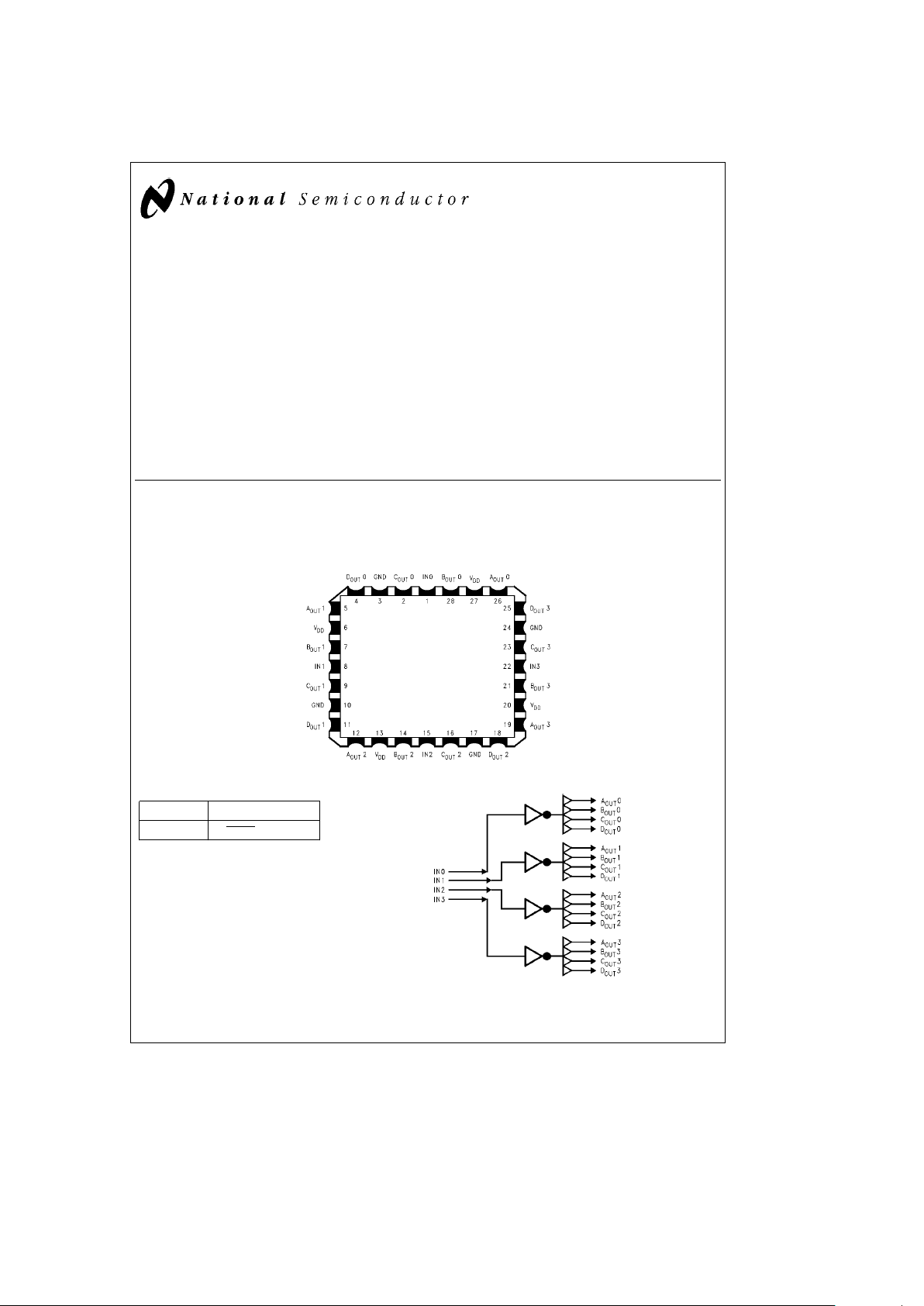
Connection Diagrams
Pin Assignment for 28-Pin PLCC
TL/F/11921– 5
Truth Table
Input Output
ln(0–3) ABCD Out (0–3)
CGS2534
TL/F/11921– 1
C
1995 National Semiconductor Corporation RRD-B30M115/Printed in U. S. A.
Page 2
Absolute Maximum Ratings (Note)
If Military/Aerospace specified devices are required,
please contact the National Semiconductor Sales
Office/Distributors for availability and specifications.
Supply Voltage (V
CC
) 7.0V
Input Voltage (VI) 7.0V
Input Current
b
30 mA
Current Applied to Output (High/Low) twice the rated
I
OH/IOL
mA
Operating Temperature
Industrial Grade
b
40§Ctoa85§C
Commercial Grade 0
§
Ctoa70§C
Storage Temperature Range
b
65§Ctoa150§C
Airflow Typical i
JA
0 LFM 62§C/W
225 LFM 43§C/W
500 LFM 34§C/W
900 LFM 27§C/W
Recommended Operating
Conditions
Supply Voltage (VCC) 4.5V to 5.5V
Maximum Input Rise/Fall Time (0.8V to 2.0V) 5 ns
Free Air Operating Temperature (T
A
)
Industrial
b
40§Ctoa85§C
Commercial 0
§
Ctoa70§C
Note:
The Absolute Maximum Ratings are those values beyond which the safety of the device cannot be guaranteed.
The device should not be operated at these limits. The parametric values defined in the DC and AC Electrical Characteristics tables are not guaranteed at the absolute maximum
ratings. The Recommended Operating Conditions will define the conditions for actual device operation.
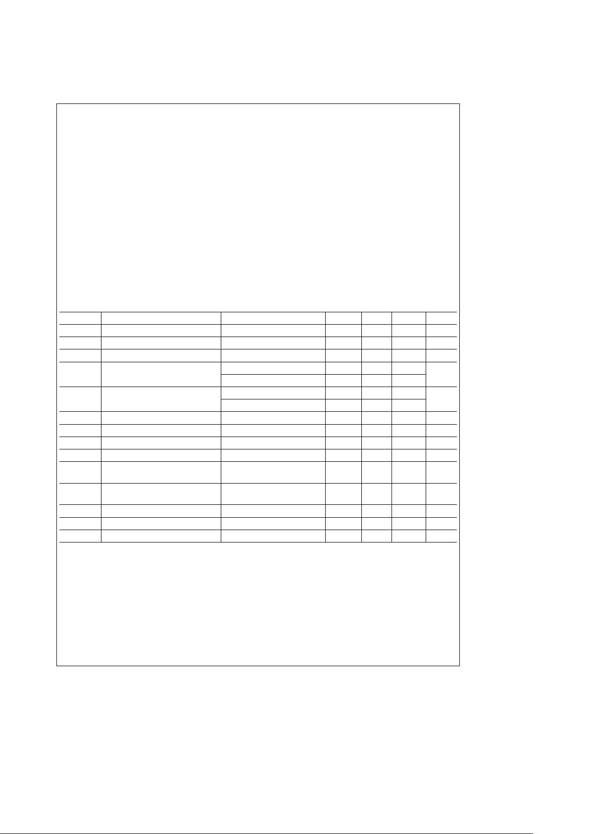
DC Electrical Characteristics
Over recommended operating conditions unless otherwise specified. All typical values are measured at V
CC
e
5V, T
A
e
25§C
Symbol Parameter Conditions Min Typ Max Unit
V
IL
Input Low Level Voltage 0.8 V
V
IH
Input High Level Voltage 2.0 V
V
IK
Input Clamp Voltage V
CC
e
4.5V, I
I
eb
18 mA
b
1.2 V
V
OH
High Level Output Voltage I
OH
eb
3 mA, V
CC
e
4.5V 2.4
V
(Note 5)
I
OH
eb
36 mA, V
CC
e
4.5V 2.0
V
OL
Low Level Output Voltage V
CC
e
4.5V, I
OL
e
36 mA 0.4 0.5
V
(Note 5)
V
CC
e
4.5V, I
OL
e
50 mA 0.1 0.1
I
I
Input Current@Max Input Voltage V
CC
e
5.5V, V
IH
e
7V 7 mA
I
IH
High Level Input Current V
CC
e
5.5V, V
IH
e
2.7V 5 mA
I
IL
Low Level Input Current V
CC
e
5.5V, V
IL
e
0.4V
b
5 mA
I
OS
Output Drive Current V
CC
e
5.5V, V
O
e
0V
b
100 275 mA
I
OLD
Minimum Dynamic Output Current V
CC
e
5.5V, V
OLD
e
0.8V
70 mA
(Note 1)
I
OHD
Minimum Dynamic Output Current V
CC
e
5.5V, V
OHD
e
2.0V
b
90 mA
(Note 1)
I
CCT
Maximum ICC/Input V
CC
e
5.5V 3.6 mA
I
CC
Supply Current ’2534 (Quiescent) V
CC
e
5.5V 235 mA
C
IN
Input Capacitance V
CC
e
5V 5 pF
Note 1: Maximum test duration 2.0 ms, one output loaded at a time.
2
Page 3

AC Electrical Characteristics
Over recommended operating conditions unless otherwise specified. All typical values are measured at V
CC
e
5V, T
A
e
25§C
Symbol Parameter
CGS2534
Unit
T
A
ea
25§CT
A
eb
40§Ctoa85§C
C
L
e
50 pF C
L
e
50 pF
R
L
e
500X R
L
e
500X
Min Typ Max Min Typ Max
f
MAX
Frequency Maximum 125 MHz
t
PLH
Low-to-High Propagation Delay
3.5 3.5 ns
INnto OUT
n
t
PHL
High-to-Low Propagation Delay
3.5 3.5 ns
IN
n
to OUT
n
t
OSHL
Maximum Skew Common
Edge Output-to-Output 150 350 300 350 ps
Variation (Note 2)
t
OSLH
Maximum Skew Common
Edge Output-to-Output 150 350 300 350 ps
Variation (Note 2)
t
RISE
, Rise/Fall Time
1.5 1.5 ns
t
FALL
(from 0.8V/2.0V to 2.0V/0.8V)
t
HIGH
Pulse Width Duration High 4 4
t
LOW
Pulse Width Duration Low 4 4 ns
(Note 4)
t
PVLH
Part-to-Part Variation of
650 650 ps
Low-to-High Transitions (Note 3)
t
PVHL
Part-to-Part Variation of
650 650 ps
High-to-Low Transitions (Note 3)
Note 2: Output-to-Output Skew is defined as the absolute value of the difference between the actual propagation delay for any outputs within the same packaged
device. The specifications apply to any outputs switching in the same direction either HIGH to LOW (t
OSHL
) or LOW to HIGH (t
OSLH
). Limits are guaranteed by
design.
Note 3: Part to Part transition variation is defined as the absolute difference between the propagation delay of any output on one device to any output on another
device. The specifications apply to any outputs switching in the same direction either HIGH to LOW (t
PVHL
) or LOW to HIGH (t
PVLH
). Limits are guaranteed by
design.
Note 4: Time high is measured at 2.0V, time low is measured at 0.8V.
Note 5: For increased drive, output pins may be connected together when the corresponding input pins are connected together.
Timing Information
TL/F/11921– 2
3
Page 4

CGS2534/35/36/37
Memory Array Driving
In order to minimize the total load on the address bus, quite
often memory arrays are being driven by buffers while having the inputs of the buffers tied together. Although this
practice was feasible in the conventional memory designs,
in today’s high speed, large buswidth designs which require
address fetching at higher speeds, this technique produces
many undesired results such as cross-talk and over/undershoot.
CGS2534/35/36/37 Quad 1 to 4 Clock Drivers were designed specifically to address these application issues on
high speed, large memory arrays systems.
These drivers are optimized to driver large loads, with 3.5 ns
propagation delays. These drivers produce less noise while
reducing the total capacitive loading on the address bus by
having only four inputs tied together (see the diagram below, point A). This helps to minimize the overshoot and undershoot by having only four outputs being switched simultaneously.
Also this larger fan-out helps to save board space since for
every one of these drivers, two conventional buffers were
typically being used.
Another feature associated with these clock drivers is a
350 ps pin-to-pin skew specification. The minimum skew
specification allows high speed memory system designers
to optimize the performance of their memory sub-system by
operating at higher frequencies without having concerns
about output-to-output (bank-to-bank) synchronization problem which are associated with driving high capacitive loads
(Point B).
The diagram below depicts a ‘‘2534/35/36/37’’ a memory
subsystem operating at high speed with large memory capacity. The address bus is common to both the memory and
the CPU and I/Os.
These drivers can operate beyond 125 MHz, and are also
available in 3V –5V TTL/CMOS versions with large current
drive .
Device V
CC
I/O Output Configuration
2534 5 TTL Inverting quad 1– 4
2535 3 or 5 CMOS Non-inverting quad 1 –4
2536 3 or 5 CMOS Inverting, Non-inverting,
d
2
2537
5 TTL Inverting quad 1– 4 with series 8X output resistors
TL/F/11921– 7
4
Page 5

5
Page 6

CGS2534V Commercial/CGS2534TV Industrial
Quad 1 to 4 Clock Drivers
Physical Dimensions inches (millimeters)
28 Lead Molded Plastic Leaded Chip Carrier
Order Number CGS2534V, CGS2534TV
NS Package Number V28A
LIFE SUPPORT POLICY
NATIONAL’S PRODUCTS ARE NOT AUTHORIZED FOR USE AS CRITICAL COMPONENTS IN LIFE SUPPORT
DEVICES OR SYSTEMS WITHOUT THE EXPRESS WRITTEN APPROVAL OF THE PRESIDENT OF NATIONAL
SEMICONDUCTOR CORPORATION. As used herein:
1. Life support devices or systems are devices or 2. A critical component is any component of a life
systems which, (a) are intended for surgical implant support device or system whose failure to perform can
into the body, or (b) support or sustain life, and whose be reasonably expected to cause the failure of the life
failure to perform, when properly used in accordance support device or system, or to affect its safety or
with instructions for use provided in the labeling, can effectiveness.
be reasonably expected to result in a significant injury
to the user.
National Semiconductor National Semiconductor National Semiconductor National Semiconductor
Corporation Europe Hong Kong Ltd. Japan Ltd.
1111 West Bardin Road Fax: (
a
49) 0-180-530 85 86 13th Floor, Straight Block, Tel: 81-043-299-2309
Arlington, TX 76017 Email: cnjwge@tevm2.nsc.com Ocean Centre, 5 Canton Rd. Fax: 81-043-299-2408
Tel: 1(800) 272-9959 Deutsch Tel: (
a
49) 0-180-530 85 85 Tsimshatsui, Kowloon
Fax: 1(800) 737-7018 English Tel: (
a
49) 0-180-532 78 32 Hong Kong
Fran3ais Tel: (
a
49) 0-180-532 93 58 Tel: (852) 2737-1600
Italiano Tel: (
a
49) 0-180-534 16 80 Fax: (852) 2736-9960
National does not assume any responsibility for use of any circuitry described, no circuit patent licenses are implied and National reserves the right at any time without notice to change said circuitry and specifications.
 Loading...