

Page 1

CEM4042
N-Channel Enhancement Mode Field Effect Transistor
FEATURES
40V, 18A, R
R
Super high dense cell design for extremely low R
High power and current handing capability.
Lead free product is acquired.
Surface mount Package.
ABSOLUTE MAXIMUM RATINGS T
Drain-Source Voltage
Gate-Source Voltage
Drain Current-Continuous
Drain Current-Pulsed
Maximum Power Dissipation
Operating and Store Temperature Range TJ,Tstg -55 to 150
= 5.1mΩ @VGS = 10V.
DS(ON)
= 7.5mΩ @VGS = 4.5V.
DS(ON)
Parameter
a
SO-8
.
DS(ON)
1
= 25 C unless otherwise noted
A
Symbol Limit
V
DS
V
GS
I
D
I
DM
P
D
D D D D
8 7 6 5
1 2 3 4
S S S G
40
±20
18
72
2.5
PRELIMINARY
Units
V
V
A
A
W
C
Thermal Characteristics
Parameter Symbol Limit Units
Thermal Resistance, Junction-to-Ambient
Details are subject to change without notice .
b
Rev 1. 2010.OctThis is preliminary information on a new product in development now .
http://www.cetsemi.com
1
C/W50RθJA
Page 2
CEM4042
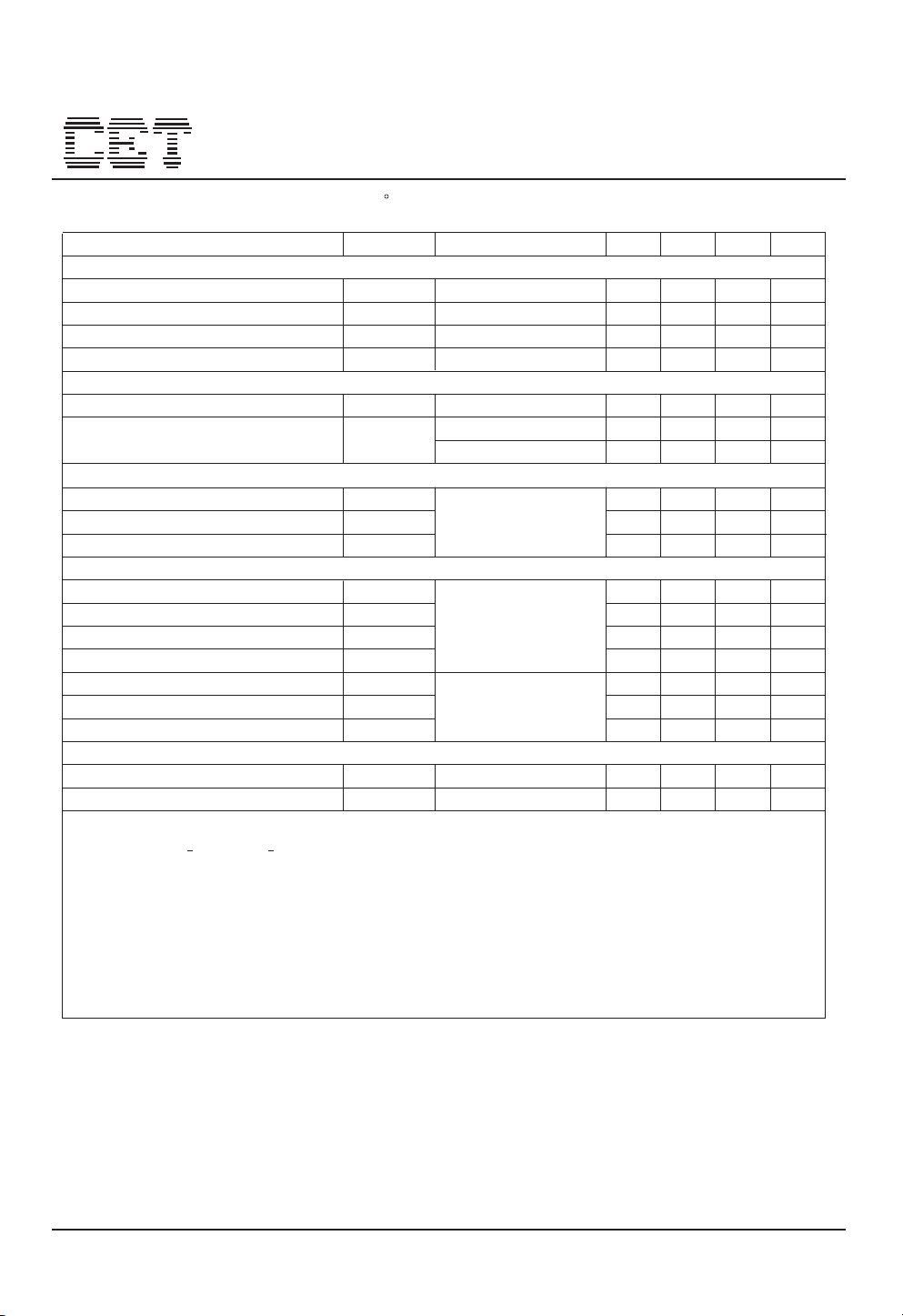
Electrical Characteristics T
= 25 C unless otherwise noted
c
Parameter Symbol Min Units
Off Characteristics
Drain-Source Breakdown Voltage
Zero Gate Voltage Drain Current
Gate Body Leakage Current, Forward
Gate Body Leakage Current, Reverse
BV
I
DSS
I
GSSF
IGSSR
DSS
On Characteristics
Gate Threshold Voltage
Static Drain-Source
On-Resistance
Dynamic Characteristics
c
Input Capacitance
Output Capacitance
Reverse Transfer Capacitance
Switching Characteristics
c
Turn-On Delay Time
Turn-On Rise Time
Turn-Off Delay Time
Turn-Off Fall Time
Total Gate Charge
Gate-Source Charge
Gate-Drain Charge
V
GS(th)
R
DS(on)
C
C
C
t
d(on)
t
d(off)
Q
Q
iss
oss
rss
t
r
t
f
Q
g
gs
gd
Drain-Source Diode Characteristics and Maximun Ratings
Drain-Source Diode Forward Current
Drain-Source Diode Forward Voltage
Notes :
a.Repetitive Rating : Pulse width limited by maximum junction temperature.
b.Pulse Test : Pulse Width < 300µs, Duty Cycle < 2%.
c.Guaranteed by design, not subject to production testing.
b
I
S
V
SD
Test Condition
VGS = 0V, ID = 250µA
Typ Max
40
VDS = 40V, VGS = 0V
VGS = 20V, VDS = 0V
VGS = -20V, VDS = 0V
VGS = VDS, ID = 250µA
VGS = 10V, ID = 10A
1 3
4.2
VGS = 4.5V, ID = 8A 5.7
VDS = 15V, VGS = 0V,
f = 1.0 MHz
4105
670
455
36
VDD = 15V, ID = 15A,
VGS = 4.5V,
R
= 1.8Ω
GEN
VDS = 15V, ID = 15A,
VGS = 4.5V
36
59
29
53
13
25
VGS = 0V, IS = 2.5A
1
100
-100
5.1
7.5
72
72
118
58
69
2.5
1
V
µA
nA
nA
V
mΩ
mΩ
pF
pF
pF
ns
ns
ns
ns
nC
nC
nC
A
V
2
Page 3
CEM4042
10
VGS=10,8,6V
8
6
4
ID, Drain Current (A)
2
0
0 0.2
0.4
VDS, Drain-to-Source Voltage (V)
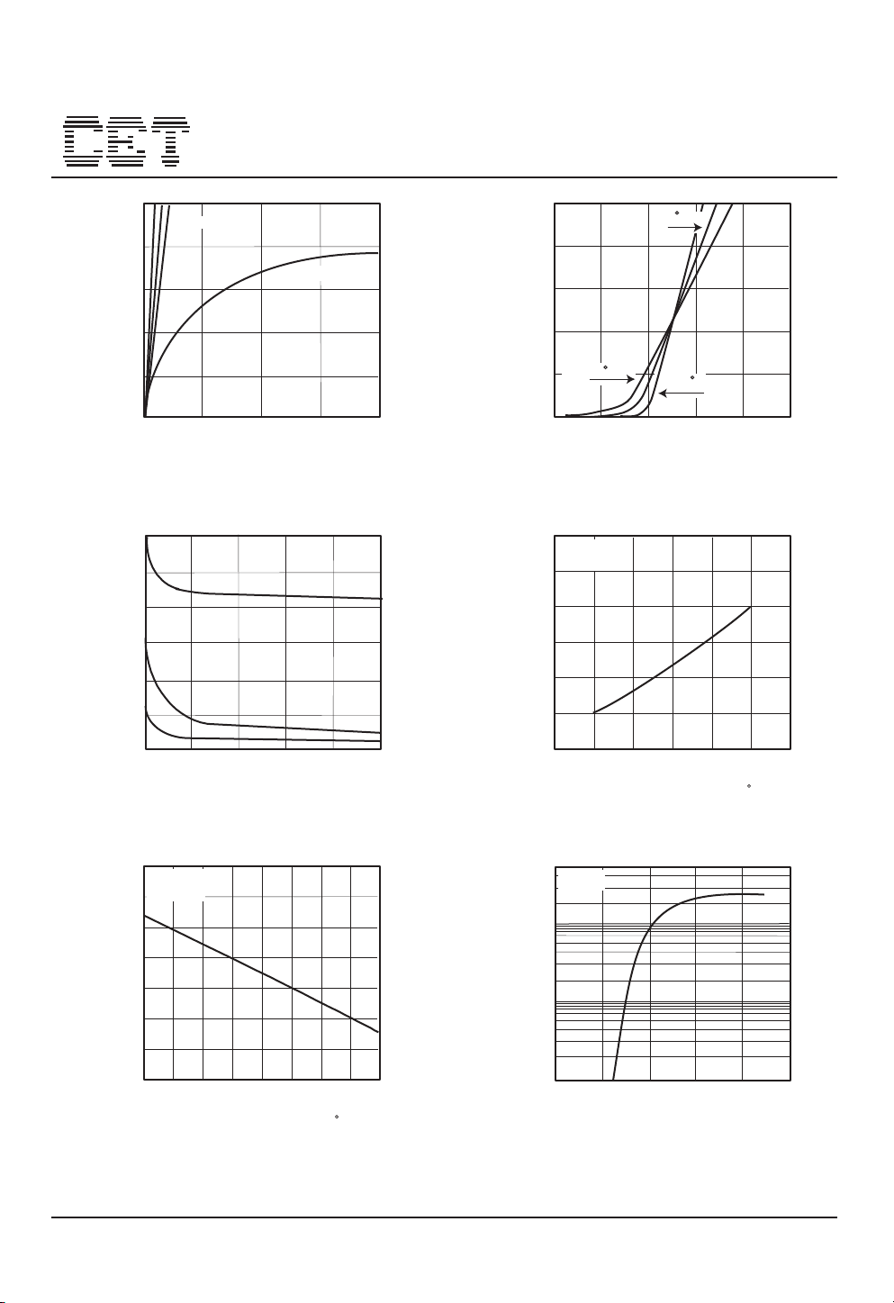
Figure 1. Output Characteristics
6000
5000
4000
3000
2000
C, Capacitance (pF)
1000
C
rss
0
0 5 10 15 20 25
C
iss
C
oss
VDS, Drain-to-Source Voltage (V)
0.6
40
32
V
=3V
GS
0.8
24
16
ID, Drain Current (A)
TJ=125 C
8
0
1.5 3 4.5 60 7.5
25 C
-55 C
VGS, Gate-to-Source Voltage (V)
Figure 2. Transfer Characteristics
2.2
ID=10A
VGS=10V
1.9
1.6
1.3
1.0
RDS(ON), Normalized
0.7
RDS(ON), On-Resistance(Ohms)
0.4
-100 -50 0 50 100 150 200
TJ, Junction Temperature( C)
Figure 3. Capacitance
1.3
VDS=V
GS
ID=250µA
1.2
1.1
1.0
0.9
0.8
VTH, Normalized
0.7
Gate-Source Threshold Voltage
0.6
-50 -25 0 25 50 75 100 125 150
TJ, Junction Temperature( C)
Figure 5. Gate Threshold Variation
with Temperature
Figure 4. On-Resistance Variation
with Temperature
V
=0
V
GS
1
10
0
10
IS, Source-drain current (A)
-1
10
0.4 0.6 0.8 1.0
1.41.2
VSD, Body Diode Forward Voltage (V)
Figure 6. Body Diode Forward Voltage
Variation with Source Current
3
Page 4

CEM4042
5
VDS=15V
ID=15A
4
3
2
1
VGS, Gate to Source Voltage (V)
0
0 15 30 45 60
Qg, Total Gate Charge (nC)
Figure 7. Gate Charge
DD
V
IN
V
D
V
GS
GEN
R
G
S
2
10
R
Limit
DS(ON)
1
10
0
10
-1
10
ID, Drain Current (A)
-2
10
TA=25 C
TJ=150 C
Single Pulse
-2
10
-1
10
10ms
100ms
1s
DC
0
10
1
10
2
10
VDS, Drain-Source Voltage (V)
Figure 8. Maximum Safe
Operating Area
on
t
d(off)
t
r
t
90%
10% 10%
INVERTED
50% 50%
V
V
d(on)
t
OUT
IN
10%
R
L
OUT
V
90%
t
off
f
t
90%
PULSE WIDTH
Figure 9. Switching Test Circuit
0
10
D=0.5
0.2
-1
0.1
10
0.05
0.02
0.01
-2
10
r(t),Normalized Effective
Single Pulse
Transient Thermal Impedance
-3
10
-4
10
-3
10
Figure 11. Normalized Thermal Transient Impedance Curve
Figure 10. Switching Waveforms
-2
10
-1
10
Square Wave Pulse Duration (sec)
4
PDM
t1
t2
1. RθJA (t)=r (t) * RθJA
2. RθJA=See Datasheet
3. TJM-TA = P* RθJA (t)
4. Duty Cycle, D=t1/t2
0
10
1
10
2
10
 Loading...