

Page 1
CDP68HC68W1
March 1998
Features
• Programmable Frequency and Duty Cycle Output
• Serial Bus Input; Compatible with Motorola/Intersil
SPI Bus, Simple Shift-Register Type Interface
• 8 Lead PDIP Package
• Schmitt Trigger Clock Input
o
• 4V to 6V Operation, -40
C to 85oC Temperature Range
• 8MHz Clock Input Frequency
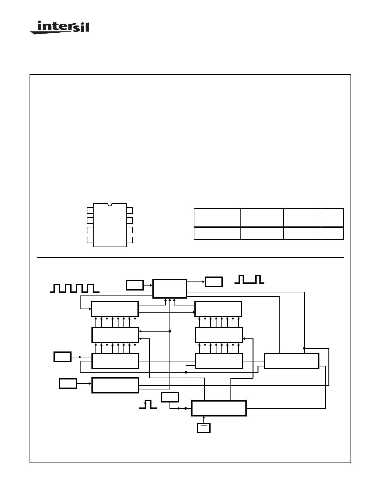
Pinout
CDP68HC68W1
(PDIP)
TOP VIEW
CLK
1
2
CS
3
V
T
V
4
SS
8
V
DD
7
PWM
6
SCK
5
DAT A
CMOS Serial Digital Pulse Width Modulator
Description
The CDP68HC68W1 modulates a clock input to supply a
variable frequency and duty-cycle output signal. Three 8-bit
registers (pulse width, frequency and control) are accessed
serially after power is applied to initialize device operation.
The value in the pulse width register selects the high
duration of the output period. The frequency register byte
divides the clock input frequency and determines the overall
output clock period. The input clock can be further divided by
two or a low power mode may be selected by the lower two
bits in the control register. A comparator circuit allows
threshold control by setting the output low if the input at the
V
pin rises above 0.75V. The CDP68HC68W1 is supplied in
T
an 8 lead PDIP package (E suffix).
Ordering Information
TEMP. RANGE
PART NUMBER
CDP68HC68W1E -40 to 85 8 Ld PDIP E8.3
(oC) PACKAGE
PKG.
NO.
Block Diagram
DAT A
V
T
8 - STAGE RIPPLE
COUNTER
PULSE - WIDTH
DATA REGISTER
8 - STAGE SHIFT
REGISTER
V
T
COMPARATOR
CLK
RESET
LOAD
INPUT CLK
MODULATOR
LOGIC
SCK
PWM
8 - STAGE RIPPLE
COUNTER
FREQUENCY
DATA REGISTER
8 - STAGE SHIFT
REGISTER
168
5 - STAGE 24 - STATE
COMPARATOR
CS
LOAD
24
CONTROL REGISTER
2 - STAGE SHIFT
LOAD
CAUTION: These devices are sensitive to electrostatic discharge; follow proper IC Handling Procedures.
http://www.intersil.com or 407-727-9207
| Copyright © Intersil Corporation 1999
1
File Number 1919.3
Page 2
CDP68HC68W1
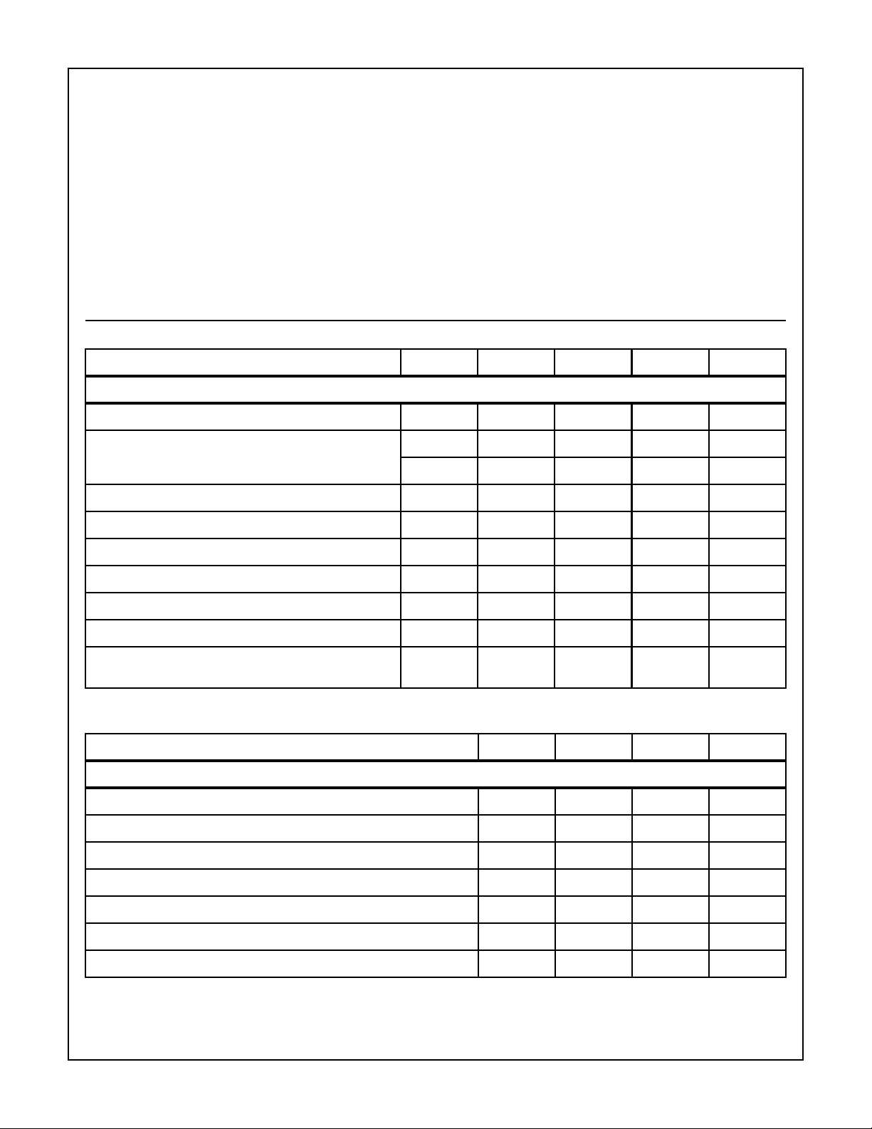
Absolute Maximum Ratings Thermal Information
DC Supply Voltage Range, (VDD) . . . . . . . . . . . . . . . . -0.5V to +7V
(Voltage Referenced to VSS Terminal)
Input Voltage Range, All Inputs . . . . . . . . . . . . .-0.5V to VDD +0.5V
DC Input Current, Any One Input. . . . . . . . . . . . . . . . . . . . . . . . .±10mA
Operating Conditions
Temperature Range (TA) . . . . . . . . . . . . . . . . . . . . . . -40oC to 85oC
TA = Full Package Temperature Range (All Package Types)
CAUTION: Stresses above those listed in “Absolute Maximum Ratings” may cause permanent damage to the device. This is a stress only rating and operation
of the device at these or any other conditions above those indicated in the operational sections of this specification is not implied.
NOTE:
1. θJA is measured with the component mounted on an evaluation PC board in free air.
DC Electrical Specifications
PARAMETER SYMBOL MIN TYP MAX UNITS
CDP68HC68W1, VDD = 5V ±10%, VSS = 0V, TA = -40oC to 85oC
DC Operating Voltage Range - 4 - 6 V
Thermal Resistance (Typical, Note 1) θJA (oC/W)
PDIP Package. . . . . . . . . . . . . . . . . . . . . . . . . . . . . 99
Device Dissipation Per Output Transistor . . . . . . . . . . . . . . .100mW
Maximum Storage Temperature Range (T
) . . . .-65oC to 150oC
STG
Maximum Lead Temperature (During Soldering) . . . . . . . . . . 265oC
At Distance 1/16 ±1/32 in. (1.59 ± 0.79mm)
From Case for 10s Max
Input Voltage Range (Except VT Pin) V
VT Pin Output Voltage Threshold V
Device Current in “Power Down” Mode, Clock Disabled I
Low Level Output Voltage (IOL = 1.6mA) V
High Level Output Voltage (IOH = -1.6mA) V
Input Leakage Current I
Operating Device Current (f
= 1MHz) I
CLK
OPER
Clock Input Capacitance
(VIN = 0V, f
= 1MHz, TA = 25oC)
CLK
IH
V
IL
IT
PD
OL
OH
IN
C
IN
0.7•V
DD
-0.3 - 0.3•V
0.4 - 0.15•V
-V
+0.3V V
DD
DD
DD
--1µA
- - 0.4 V
VDD - 0.4V - - V
--±1 µA
--1mA
- - 10 pF
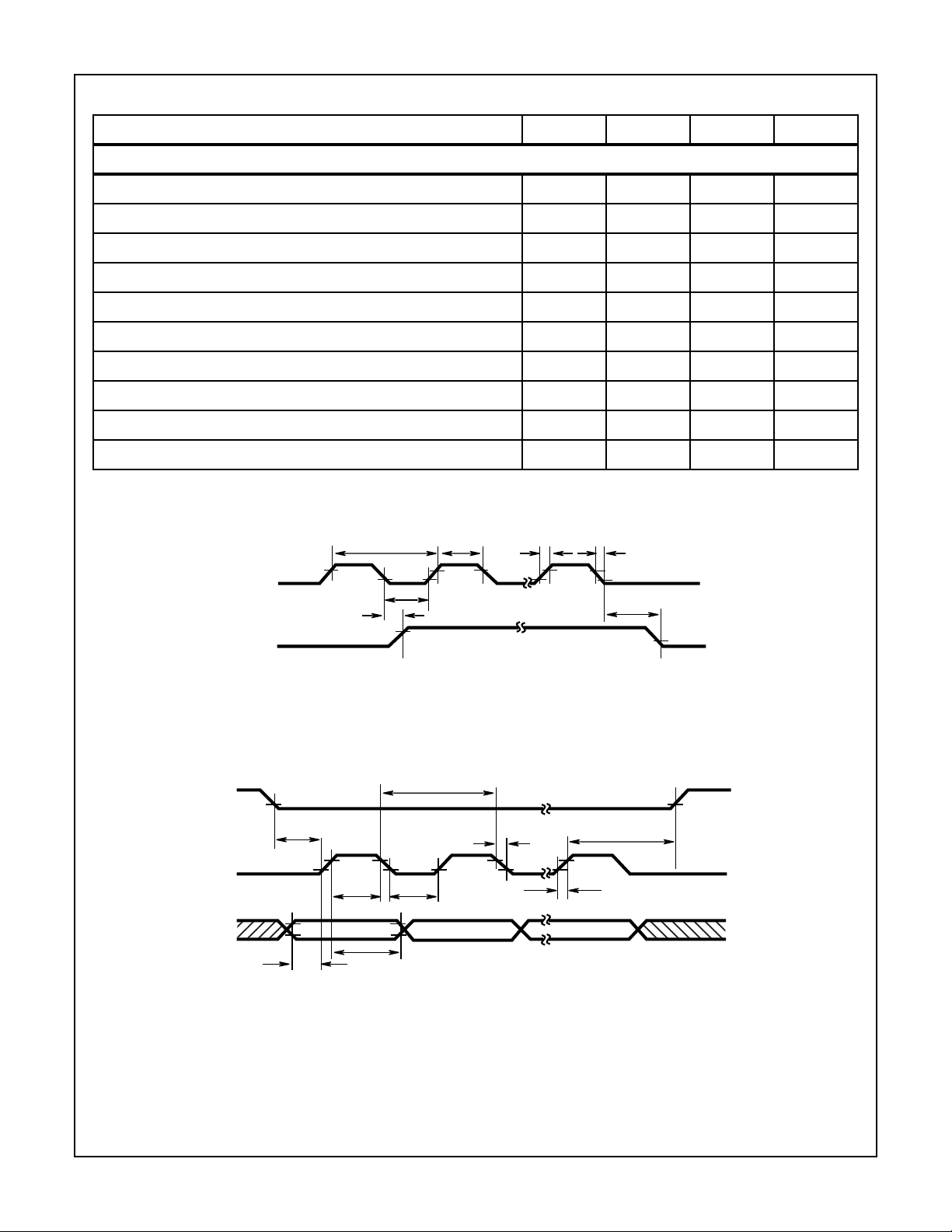
Control Timing
PARAMETER SYMBOL MIN MAX UNITS
CDP68HC68W1, VDD = 5V ±10%, VSS = 0V, TA = -40oC to 85oC
Clock Frequency F
Cycle Time t
Clock to PWM Out t
Clock High Time t
Clock Low Time t
Rise Time (20% VDD to 70% VDD)t
Fall Time (70% VDDto 20% VDD)t
CLK
CYC
PWMO
CLKH
CLKL
R
F
DC 8.0 MHz
--ns
- 125 ns
50 - ns
50 - ns
- 100 ns
- 100 ns
V
V
2
Page 3
CDP68HC68W1
SPI Interface Timing
PARAMETER SYMBOL MIN MAX UNITS
CDP68HC68W1, VDD = 5V ±10%, VSS = 0V, TA = -40oC to 85oC
Serial Clock Frequency f
Cycle Time t
Enable Lead Time t
Enable Lag Time t
Serial Clock (SCK) High Time t
Serial Clock (SCK) Low Time t
Data Setup Time t
Data Hold Time t
Fall Time (70% VDD to 20% VDD, CL = 200pF) t
Rise Time (20% VDD to 70% VDD, CL = 200pF) t
t
CLKH
t
R
CLK
t
PWMO
t
CYC
t
CLKL
SCK
SCYC
ELD
ELG
SH
SL
DSU
DHD
SCKF
SCKR
DC 2.1 MHz
480 - ns
240 - ns
- 200 ns
190 - ns
190 - ns
100 - ns
100 - ns
- 100 ns
- 100 ns
t
F
t
PWMO
CS
(INPUT)
SCK
(INPUT)
DAT A
(INPUT)
PWM
FIGURE 1. PWM TIMING
t
SCYC
t
ELD
t
DSU
t
SH
MSB LSB
t
DHD
t
SCKF
t
SL
FIGURE 2. SERIAL PERIPHERAL INTERFACE TIMING
t
t
SCKR
ELG
3
Page 4

CDP68HC68W1
CHIP SELECT
PWM-OUT = 0
CS)
(
SERIAL CLK
(SCK)
DAT A
CLK = 0
CS)
(
SCK
DAT A
CLK
PWM-OUT
CONTROL WORD FREQUENCY WORD
DON’T
DON’T
DON’T
DON’T
DON’T
DON’T
CARE
CARE
FREQUENCY WORD PULSE WIDTH (PWM) WORD
= 0
BIT 2
= 1
= 0
BIT 1
CARE
= 0
= 0
CARE
BIT 0
= 0
= 0
BIT 7
CARE
= 0
= 0
CARE
BIT 6
= 0
PWR
COUNT
BIT 5
= 0
LSB MSBMSB
CLOCK
DIVIDE
BIT 4
= 0
BIT 7
= 0
= 0= 0= 0
BIT 2
BIT 3
= 0
= 0
BIT 6
= 0
BIT 5
BIT 1
= 0
= 0
LSBMSBLSB
BIT 4
01234567012
BIT 0
= 1
= 0
3456701234567
BIT 3
= 0
CURVES
CONTINUED
IMMEDIATELY
BELOW
CURVES
CONTINUED
BELOW
CLK
PWM
OUT
TOTAL OUTPUT PERIOD =
5 X (INPUT CLOCK PERIOD)
FIGURE 3. CDP68HC68W1 INTERFACE TIMING SPECIFICATIONS (CONTINUED)
INPUT
CLOCK (CLK)
OUTPUT
(PWM)
4
Page 5

CDP68HC68W1
Introduction
The digital pulse width modular (DPWM) divides down a
clock signal supplied via the CLK input as specified by the
control, frequency, and pulse width data registers. The
resultant output signal, with altered frequency and duty
cycle, appears at the output of the device on the PWM pin.
Functional Pin Description
VDD and V
These pins are used to supply power and establish logic levels within the PWM. V
V
SS
CLK
The CLK pin is an input only pin where the clock signal to be
altered by the PWM circuitry is supplied. This is the source
of the PWM output. This input frequency can be internally
divided by either one or two, depending on the state of the
CD bit in the control register.
CS
The CS pin is the chip select input to the PWM’s SPI interface. A high-to-low (1 to 0) transition selects the chip. A lowto-high (0 to 1) transition deselects the chip and transfers
data from the shift registers to the data registers.
VT
The VT pin is the input to the voltage threshold comparator
on the PWM. An analog voltage greater than 0.75V (at V
= 5V) on this pin will immediately cause the PWM output to
go to logic “0”. This will be the status until the V
returned to a voltage below 0.4V, the W1 is deselected, and
then one or more of the data registers is written to.
An analog voltage on this pin less than 0.75V (at V
will allow the device to operate as specified by the values in
the registers.
DAT A
Data input at this pin is clocked into the shift register (i.e.,
latched) on the rising edge of the serial clock (SCK), most
significant bits first.
SCK
The SCK pin is the serial clock input to the PWM’s SPI interface. A rising edge on this pin will shift data available at the
(DATA) pin into the shift register.
PWM
This pin provides the resultant output frequency and pulse
width. After V
a logic “0”, until the chip is selected, 24 bits of information
clocked in, and the chip deselected.
SS
(ground).
is a positive voltage with respect to
DD
input is
T
DD
power up, the output on this pin will remain
DD
DD
= 5V)
Functional Description
Serial Port
Data are entered into the three DPWM registers serially
through the DATA pin, accompanied by a clock signal applied
to the SCK. The user can supply these serial data via shift
register(s) or a microcontroller’s serial port, such as the SPI
port available on most CDP68HC05 microcontrollers. Microcontroller I/O lines can also be used to simulate a serial port.
Data are written serially, most significant bit first, in 8, 16 or
24-bit increments. Data are sampled and shifted into the
PWMs shift register on each rising edge of the SCK. The
serial clock should remain low when inactive. Therefore,
when using a 68HC05 microcontroller’s SPI port to provide
data, program the microcontroller’s SPI control register bits
CPOL, CPHA to 0, 0.
The CDP68HC68W1 latches data words after device
deselection. Therefore,
each write to the W1.
Power-Up Initialization
Upon V
at a low level (logic zero) until:
1. The chip is selected (
2. 24-bit of information are shifted in.
3. The chip is deselected (
The 24-bits of necessary information pertain to the loading
of the PWM 8-bit registers, in the following order:
1. Control register
2. Frequency register
3. Pulse width register
See section entitled
ters
specified PWM output signal will appear until the device is
reprogrammed or the voltage on the V
specified threshold. Reprogramming the device will update
the PWM output after the end of the present output clock
period.
Reprogramming Shortcuts
After the device has been fully programmed upon power up,
it is only necessary to input 8 bits of information to alter the
output pulse width, or 16 bits to alter the output frequency.
Altering the Pulse Width: The pulse width may be
changed by selecting the chip, inputting 8 bits, and deselecting the chip. By deselecting the chip, data from the first
8-bit shift register are latched into the pulse width register
(PWM register). The frequency and control registers
remain unchanged. The updated PWM information will
appear at the output only after the end of the previous total
output period.
Altering the Frequency: The frequency can be changed by
selecting the chip, inputting 16 bits (frequency information
followed by pulse width information), and deselected the
power up, the output of the PWM chip will remain
DD
for a description of each register. Once initialized, the
CS must go high (inactive) following
CS pin pulled low).
CS pin pulled high).
Pulse Width Modulator Data Regis-
pin rises above the
T
5
Page 6

CDP68HC68W1
chip. Deselection will transfer 16 bits of data from the shift
register into the frequency register and PW register. The
updated frequency and PW information will appear at the
PWM output pin only after the end of the previous total
output period.
Altering the Control Word: Changing the clock divider
and/or power control bit in the CDPHC68W1 control register
requires full 24-bit programming, as described under Power
Up Initialization.
Pulse Width Modulator Data Registers
Byte 1: Control Register
7654 3 210
0 0 0 0 0 0
B7-B2 Unused; “don’t care”.
B2, PC Power Control Bit. If this bit is a “0”, the chip will
remain in the active state. If the bit is set to a “1”,
internal clocking and the voltage comparator
(VT) circuit and voltage reference will be
disabled. Thus the chip will enter a low current
drain mode. The chip may only reenter the
active mode by clearing this bit and clocking in a
full 24 bits of information.
B0, CD Clock Divider Bit. If this bit is a “0”, the chip will
set internal clocking (CLK) at a divide-by-one
rate with respect to the (CLK). If this bit is set to
“1”, the internal clocking will be set to divide-by-2
state.
Byte 2: Frequency Data Register
765 4 3 210
PWM Frequency Register
B7-B0 This register contains the value that will deter-
mine the output frequency or total period by:
F
F
OUT
F
= resultant PWM output frequency
OUT
= the frequency of input CLK
F
IN
IN
------------------------------------------ -=
N1+()CD 1+()
n = value in frequency register
CD = value of clock divider bit in control register.
PC CD
Byte 3: Pulse Width Data Register
765 4 3 210
Pulse Width Data Register
B7-B0 This register contains the value that will
determine the pulse width or duty cycle (high
duration) of the output PWM waveform.
PW = (N+1) (CD+1)
PW = Pulse width out as measured in number of
input CLK periods.
CD = Value of clock divider bit in control register.
N = Value in PW register.
For a case of n (binary value in PW register)
equal to 3 and CD (clock divider) = 0 (divide-by-
1), the output will be 4 input clock periods of a
high level f ollo wed b y the remaining cloc ks of the
total period which will be a low level.
Assuming the frequency register contains a
value of 5, the resultant PWM output would be
high for 4 CLK periods, low for 2.
Using the CDP68HC68W1
Programming the CDP68HC68W1
1. Select chip
2. Write to control register
3. Write to frequency register
4. Write to pulse width register
5. Deselect chip
NEXT - TO then alter the pulse width
1. Select chip
2. Write to pulse width register*
3. Deselect chip
OR - To then alter the frequency (and possibly PW):
1. Select chip
2. Write to frequency register*
3. Write to pulse width register*
4. Deselect chip
NOTE: All writes use 8-bit words
Example
For a case of n (binary value in frequency
register) equal to 5, CD (clock divider) = 0
(divide-by-1), the PWM output will be a frequency 1/6 that of the input clock (CLK). Likewise, the output clock period will be equal to 6
input CLK periods.
when CD = 0,
When CD=0, frequency register = 4, pulse width register = 1;
output = high for 2 input CLK periods, low for 3;
1. Select chip
2. Then write (most significant bit first) to the control, the frequency, and pulse width registers (control = 00, frequency =
04, PW = 1)
6
Page 7

CDP68HC68W1
3. Deselect the chip
New pulse width out begins and PWM goes high when
CS is
raised after last SCK pulse (assuming no previous time-out).
PWM then toggles on falling CLK edges.
Resulting output waveform: Control = 00 = Divide-by-1,
frequency = 4;
PW = 1: (1 + 1) (0 + 1) = 2 CLKs high time.
CDP68HC68W1 Application Example
Frequency
INPCLK
------------------------------------- -
==
04 1+()0 1+()
INPCLK
----------------------- -
5
The following example was written for a system which has
the CDP68HC68W1 connected to the SPI bus of a
CDP68HC05C8B microcontroller. The program sets the W1
to run a divide by 200 frequency with a duty cycle of 30% by
and the Pulse Width Data Register. The frequency and pulse
width are then modified. Finally the pulse width is modified
without changing the frequency. The program was assembled using the Intersil HASM 3.0 assembler.
writing to the Control Register, the Frequency Data Register,
INTERSIL Corporation (c)1990 - 1997
68HC05 Assembler Version 3.0.2
Filename: W1.LST
Source Created: 01/08/98, 10:36 am
Assembled: 01/08/98, 10:36 am
00001 ***********************************************************************
00002 * File: W1.S
00003 * Example W1 routines - sets W1 to a divide by
00004 * 200 output with 30% duty cycle
00005 *
00006 * Date: Thursday, January 8, 1998
00007 ***********************************************************************
00008
00009 ***********************************************************************
00010 * Partial Map of CDP68HC05C8B Hardware Registers
00011 ***********************************************************************
00012
00013 0000 Section Registers, $0000
00014 0000 PortA ds 1 ;Port A
00015 0001 PortB ds 1 ;Port B
00016 0002 PortC ds 1 ;Port C
00017 0003 PortD ds 1 ;Port D
00018 0004 DDRA ds 1 ;Port A Data Direction Register
00019 0005 DDRB ds 1 ;Port B DDR
00020 0006 DDRC ds 1 ;Port C DDR
00021 0007 _Free1 ds 3 ;three unused locations
00022 000A SPCR ds 1 ;SPI Control Register
00023 $0006 = 6 SPE equ 6 ;SPI Enable bit
00024 $0004 = 4 MSTR equ 4 ;SPI Master Mode bit
00025 000B SPSR ds 1 ;SPI Status Register
00026 $0007 = 7 SPIF equ 7 ;SPI Flag bit for ANDs, CMPs, etc.
00027 000C SPDR ds 1 ;SPI Data Register
00028
00029 ***********************************************************************
00030 * CDP68HC68W1 Constants
00031 ***********************************************************************
00032
00033 $0000 = 0 W1 equ 0 ;W1 is connected to bit 0 of Port A
00034 $0002 = 2 W1_PC equ 2 ;Power Control: 1 = power down
00035 $0001 = 1 W1_CD equ 1 ;Clock Divider: 1 = divide by 2
00036
00037
00038 ***********************************************************************
00039 * Main Routines
00040 ***********************************************************************
00041
00042 0100 Section Code, $0100
00043
00044* [6] 0100 AD37 jsr Init_W1 ;turn on PA0
00045 Set200_30
00046 [5] 0102 1100 bclr W1,PortA ;select W1 (CE is active low)
00047* [6] 0104 AD28 jsr Set_SPI_Mode ;Setup the 68HC05 SPI control
00048 ;to talk to the W1
00049
00050 ******* Set Up Control, Frequency, and Pulse Width
00051
00052 SendCommands
00053 [2] 0106 A601 lda #W1_CD ;set divide by two clock on W1
7
Page 8

CDP68HC68W1
00054* [6] 0108 AD29 jsr SPI_xmit
00055 [2] 010A A663 lda #99 ;set frequency to divide by 2000
00056* [6] 010C AD25 jsr SPI_xmit
00057 [2] 010E A61D lda #29 ;set pulse width to 30% duty cycle
00058* [6] 0110 AD21 jsr SPI_xmit
00059
00060 DeselectW1_1
00061 [5] 0112 1000 bset W1,PortA ;deselect the W1 which loads registers
00062 ; with values transmitted
00063
00064 ;
00065 ; Here the CDP68HC05C8B would generally
00066 ; attend to other processing issues
00067 ;
00068
00069 ******* Modify Frequency and Pulse Width
00070
00071 [5] 0114 1100 bclr W1,PortA ;select W1 (CE is active low)
00072* [6] 0116 AD16 jsr Set_SPI_Mode ;Setup the CDP68HC05 SPI Control....
00073 ;to talk to the W1
00074 SendCommands2
00075 [2] 0118 A631 lda #49 ;set frequency to divide by 100 (the
00076* [6] 011A AD17 jsr SPI_xmit ;divide by 2 is still in effect)
00077 [2] 011C A609 lda #9 ;set pulse width to 20% duty cycle
00078* [6] 011E AD13 jsr SPI_xmit
00079
00080 DeselectW1_2
00081 [5] 0120 1000 bset W1,PortA ;deselect the W1 which loads registers
00082
00083 ;
00084 ; Here the CDP68HC05C8B would again
00085 ; attend to other processing issues
00086 ;
00087
00088 ******* Modify Pulse Width
00089
00090 [5] 0122 1100 bclr W1,PortA ;select W1 (CE is active low)
00091* [6] 0124 AD08 jsr Set_SPI_Mode ;Setup the 68HC05 SPI control...
00092 ;to talk to the W1
00093 SendCommands3
00094 [2] 0126 A611 lda #17 ;set pulse width to 38% duty cycle
00095* [6] 0128 AD09 jsr SPI_xmit
00096
00097 DeselectW1_3
00098 [5] 012A 1000 bset W1,PortA ;deselect the W1 which loads registers
00099 ;with values transmitted
00100 Finish
00101 [3] 012C 20FE bra * ;loop forever
00102
00103 ***********************************************************************
00104 * Common Subroutines
00105 ***********************************************************************
00106
00107 012E Section Subroutines, *
00108
00109 Set_SPI_Mode
00110 [2] 012E A650 lda #(2!SPE+2!MSTR) ;Enable SPI as a Master with....
00111 [4] 0130 B70A sta SPCR ;CPHA=CPOL=0,
00112 [6] 0132 81 rts
00113 SPI_Xmit
00114 [4] 0133 B70C sta SPDR ;send A to SPI device
00115 SPI_wait
00116 [5] 0135 0F0BFD brclr SPIF,SPSR,SPI_wait ;wait until transmit complete
00117 [6] 0138 81 rts
00118
00119 Init_W1
00120 [5] 0139 1000 bset W1,PortA ;disable the W1 (CE is active low)
00121 [5] 013B 1004 bset W1,DDRA ;by activating PA0 as a high
8
Page 9

CDP68HC68W1
Dual-In-Line Plastic Packages (PDIP)
N
D1
E1
-C-
-B-
A1
A2
A
L
e
C
S
INDEX
AREA
BASE
PLANE
SEATING
PLANE
D1
B1
1 2 3 N/2
-AD
e
B
0.010 (0.25) C AMB
NOTES:
1. Controlling Dimensions: INCH. In case of conflict between
English and Metric dimensions, the inch dimensions control.
2. Dimensioning and tolerancing per ANSI Y14.5M-1982.
3. Symbols are defined in the “MO Series Symbol List” in Section
2.2 of Publication No. 95.
4. Dimensions A, A1 and L are measured with the package seated
in JEDEC seating plane gauge GS-3.
5. D, D1, and E1 dimensions do not include mold flash or protrusions. Mold flash or protrusions shall not exceed 0.010 inch
(0.25mm).
6. E and are measured with the leads constrained to be per-
e
pendicular to datum .
A
-C-
7. eB and eC are measured at the lead tips with the leads unconstrained. eC must be zero or greater.
8. B1 maximum dimensions do not include dambar protrusions.
Dambar protrusions shall not exceed 0.010 inch (0.25mm).
9. N is the maximum number of terminal positions.
10. Corner leads (1, N, N/2 and N/2 + 1) for E8.3, E16.3, E18.3,
E28.3, E42.6 will have a B1 dimension of 0.030 - 0.045 inch
(0.76 - 1.14mm).
E8.3 (JEDEC MS-001-BA ISSUE D)
8 LEAD DUAL-IN-LINE PLASTIC PACKAGE
INCHES MILLIMETERS
SYMBOL
A - 0.210 - 5.33 4
E
A1 0.015 - 0.39 - 4
A2 0.115 0.195 2.93 4.95 -
B 0.014 0.022 0.356 0.558 -
C
L
e
A
C
e
B
B1 0.045 0.070 1.15 1.77 8, 10
C 0.008 0.014 0.204 0.355 D 0.355 0.400 9.01 10.16 5
D1 0.005 - 0.13 - 5
E 0.300 0.325 7.62 8.25 6
E1 0.240 0.280 6.10 7.11 5
e 0.100 BSC 2.54 BSC -
e
A
e
B
0.300 BSC 7.62 BSC 6
- 0.430 - 10.92 7
L 0.115 0.150 2.93 3.81 4
N8 89
NOTESMIN MAX MIN MAX
Rev. 0 12/93
All Intersil semiconductor products are manufactured, assembled and tested under ISO9000 quality systems certification.
Intersil products are sold by description only. Intersil Corporation reserves the right to make changes in circuit design and/or specifications at any time without
notice. Accordingly, the reader is cautioned to verify that data sheets are current before placing orders. Information furnished by Intersil is believed to be accurate
and reliable. However, no responsibility is assumed by Intersil or its subsidiaries for its use; nor for any infringements of patents or other rights of third parties which
may result from its use. No license is granted by implication or otherwise under an y patent or patent rights of Intersil or its subsidiaries.
For information regarding Intersil Corporation and its products, see web site http://www.intersil.com
Sales Office Headquarters
NORTH AMERICA
Intersil Corporation
P. O. Box 883, Mail Stop 53-204
Melbourne, FL 32902
TEL: (407) 724-7000
FAX: (407) 724-7240
EUROPE
Intersil SA
Mercure Center
100, Rue de la Fusee
1130 Brussels, Belgium
TEL: (32) 2.724.2111
FAX: (32) 2.724.22.05
ASIA
Intersil (Taiwan) Ltd.
Taiwan Limited
7F-6, No. 101 Fu Hsing North Road
Taipei, Taiwan
Republic of China
TEL: (886) 2 2716 9310
FAX: (886) 2 2715 3029
9
 Loading...