

Page 1
August 1997
CDP68HC68T1
CMOS Serial Real-Time Clock With
RAM and Power Sense/Control
Features
• SPI (Serial Peripheral Interface)
• Full Clock Features
- Seconds, Minutes, Hours (12/24, AM/PM), Day of
Week, Date, Month, Year (0-99), Automatic Leap Year
• 32 Word x 8-Bit RAM
• Seconds, Minutes, Hours Alarm
• Automatic Power Loss Detection
• Low Minimum Standby (Timekeeping) Voltage. . . 2.2V
• Selectable Crystal or 50/60Hz Line Input
• Buffered Clock Output
• Battery Input Pin that Powers Oscillator and also
Connects to V
Pin When Power Fails
DD
• Three Independent Interrupt Modes
- Alarm
- Periodic
- Power-Down Sense
Description
The CDP68HC68T1 Real-Time Clock provides a
time/calendar function, a 32 byte static RAM, and a 3 wire
Serial Peripheral Interface (SPI Bus). The primary function of
the clock is to divide down a frequency input that can be
supplied by the on-board oscillator in conjunction with an
external crystal or by an external clock source. The internal
oscillator can operate with a 32KHz, 1MHz, 2MHz, or 4MHz
crystal. An external clock source with a 32KHz, 1MHz,
2MHz, 4MHz, 50Hz or 60Hz frequency can be used to drive
the CDP68HC68T1. The time registers hold seconds,
minutes, and hours, while the calendar registers hold day-ofweek, date, month, and year information. The data is stored
in BCD format. In addition, 12 or 24 hour operation can be
selected. In 12 hour mode, an AM/PM indicator is provided.
The T1 has a programmable output which can provide one
of seven outputs for use elsewhere in the system.
Computer handshaking is controlled with a “wired-OR”
interrupt output. The interrupt can be programmed to provide
a signal as the result of: 1) an alarm programmed to occur at
a predetermined combination of seconds, minutes, and
hours; 2) one of 15 periodic interrupts ranging from subsecond to once per day frequency; 3) a power fail detect.
The PSE output and the V
power control. The
CPUR output is available to reset the
processor under power-down conditions.
under software control and can also be activated via the
CDP68HC68T1’s watchdog. If enabled, the watchdog
requires a periodic toggle of the CE pin without a serial
transfer.
input are used for external
SYS
CPUR is enabled
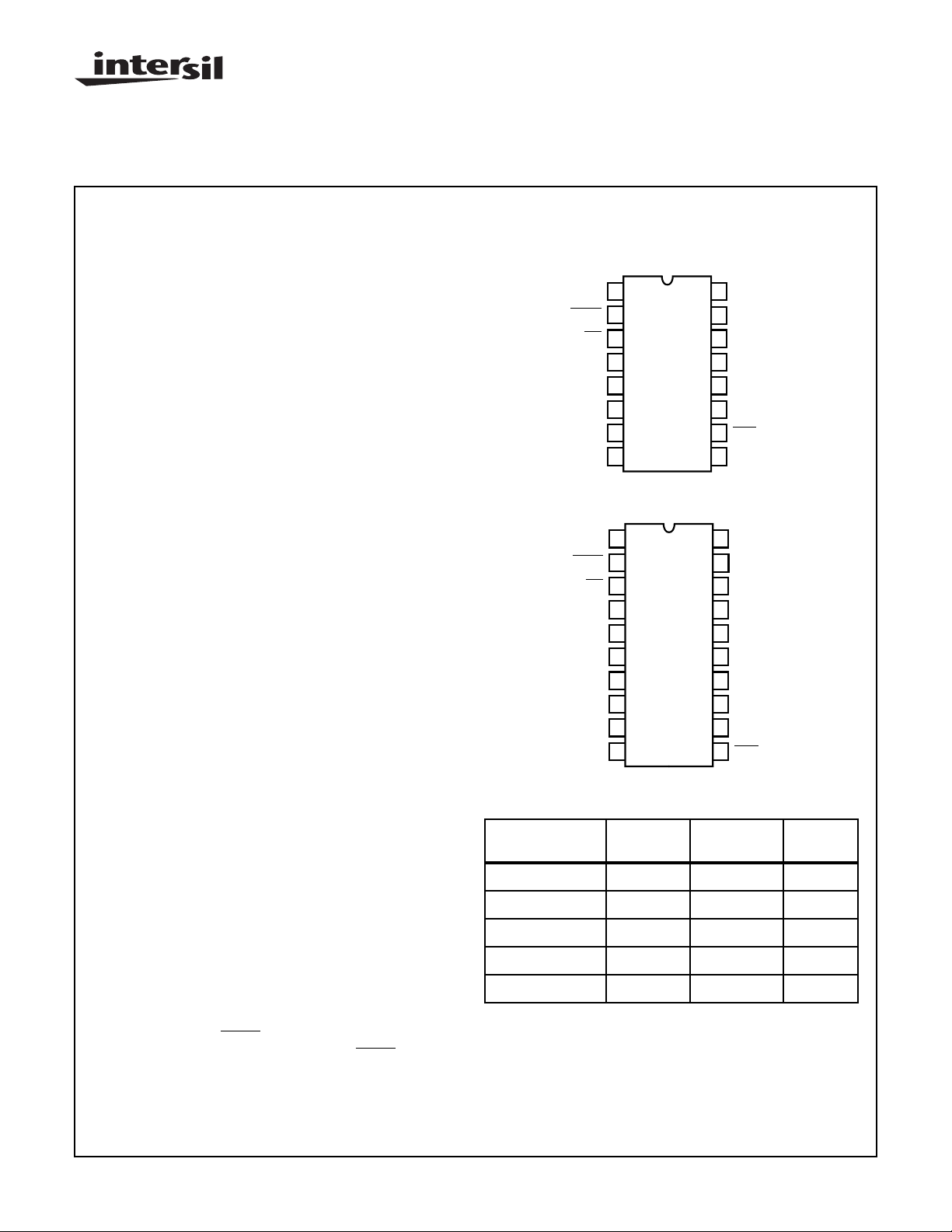
Pinouts
CDP68HC68T1 (PDIP, SBDIP, SOIC)
TOP VIEW
CLKOUT
CPUR
INT
SCK
MOSI
MISO
CE
V
SS
CLK OUT
CPUR
INT
NC
SCK
MOSI
MISO
CE
V
SS
PSE
1
2
3
4
5
6
7
8
CDP68HC68T1 (SOIC)
TOP VIEW
1
2
3
4
5
6
7
8
9
10
16
V
XTAL OUT
15
XTAL IN
14
V
13
V
12
LINE
11
POR
10
PSE
9
20
19
18
17
16
15
14
13
12
11
DD
BATT
SYS
VDD
XTAL OUT
XTAL IN
NC
V
BATT
V
SYS
NC
NC
LINE
POR
Ordering Information
TEMP.
PART NUMBER
CDP68HC68T1E -40 to 85 16 Ld PDIP E16.3
CDP68HC68T1D -40 to 85 16 Ld SBDIP D16.3
CDP68HC68T1M -40 to 85 20 Ld SOIC M20.3
CDP68HC68T1M2 -40 to 85 16 Ld SOIC M16.3
CDP68HC68T1W -40 to 85 DIE
NOTE: Pin number references throughout this specification refer to
the 16 lead PDIP/SBDIP/SOIC. See pinouts for cross reference.
RANGE (oC) PACKAGE
PKG.
NO.
CAUTION: These devices are sensitive to electrostatic discharge; follow proper IC Handling Procedures.
http://www.intersil.com or 407-727-9207
| Copyright © Intersil Corporation 1999
1
File Number 1547.3
Page 2
CDP68HC68T1
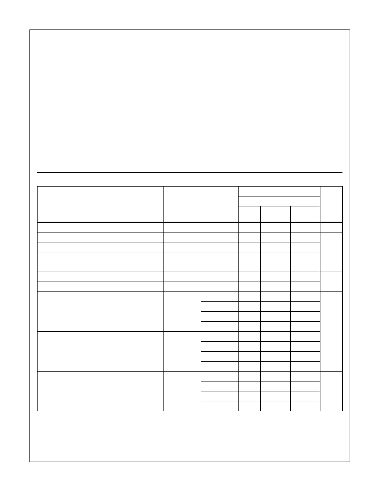
Absolute Maximum Ratings Thermal Information
Supply Voltage, VDD. . . . . . . . . . . . . . . . . . . . . . . . . . . -0.5V to +7V
Input Voltage, VIN. . . . . . . . . . . . . . . . . . . . VSS -0.3V to VDD +0.3V
Current Drain Per Input Pin Excluding VDD and VSS, I . . . . . .10mA
Current Drain Per Output Pin, I. . . . . . . . . . . . . . . . . . . . . . . . .40mA
Operating Conditions
Voltage Range . . . . . . . . . . . . . . . . . . . . . . . . . . . . . +3.0V to +6.0V
Standby (Timekeeping) Voltage . . . . . . . . . . . . . . . . +2.2V to +6.0V
Temperature Range
CDP68HC68T1D (SBDIP Package). . . . . . . . . . . -55oC to 125oC
CDP68HC68T1E (PDIP Package) . . . . . . . . . . . . . -40oC to 85oC
CDP68HC68T1M/M2 (SOIC Packages). . . . . . . . . -40oC to 85oC
Input High Voltage . . . . . . . . . . . . . . . . . . . . . . . (0.7 x VDD) to V
Input Low Voltage. . . . . . . . . . . . . . . . . . . . . . . . . .0V to (0.3 x VDD)
Serial Clock Frequency (f
CAUTION: Stresses above those listed in “Absolute Maximum Ratings” may cause permanent damage to the device. This is a stress only rating and operation
of the device at these or any other conditions above those indicated in the operational sections of this specification is not implied.
NOTE:
1. θJA is measured with the component mounted on an evaluation PC board in free air.
) . . . . . . . . . . . . . . . . . +3.0V to +6.0V
SCK
Thermal Resistance (Typical, Note 1) θJA (oC/W) θJC (oC/W)
16 Ld PDIP . . . . . . . . . . . . . . . . . . . . . 90 N/A
16 Ld SOIC . . . . . . . . . . . . . . . . . . . . . 100 N/A
20 Ld SOIC . . . . . . . . . . . . . . . . . . . . . 100 N/A
16 Ld SBDIP . . . . . . . . . . . . . . . . . . . . 75 24
Maximum Junction Temperature (Hermetic) . . . . . . . . . . . . . . . 175oC
Maximum Junction Temperature (Plastic) . . . . . . . . . . . . . . . 150oC
Maximum Storage Temperature Range (T
) . . . .-65oC to 150oC
STG
Maximum Lead Temperature (Soldering 10s) . . . . . . . . . . . . . 300oC
(SOIC, Lead Tips Only)
DD
Static Electrical Specifications At T
PARAMETER CONDITIONS
Quiescent Device Current I
Output Voltage High Level V
Output Voltage Low Level V
Output Voltage High Level V
Output Voltage Low Level V
Input Leakage Current I
Three-State Output Leakage Current I
Operating Current (Note 3)
(ID + IB) VDD = VB = 5V
Crystal Operation
Pin 14
External Clock (Squarewave) (Note 3)
(ID + IB) VDD= VS = 5V
Standby Current (Note 3) I
VS = 3V
Crystal Operation
= -40oC to +85oC, VDD = V
A
DD
OH
OL
OH
OL
IN
OUT
B
IOH = -1.6mA, VDD = 4.5V 3.7 - IOL = 1.6mA, VDD = 4.5V
IOH≤ 10µA, VDD = 4.5V 4.4 - IOL≤ 10µA, VDD = 4.5V
= 5V ±5%, except as noted.
BATT
LIMITS
CDP68HC68T1
(NOTE 2)
MIN
TYP MAX
-1 10µA
-
-
- 0.4
- 0.1
-- ±1
--±10
32kHz - 0.08 0.01
1MHz - 0.5 0.6
2MHz - 0.7 0.84
4MHz - 1 1.2
32kHz - 0.02 0.024
1MHz - 0.1 0.12
2MHz - 0.2 0.24
4MHz - 0.4 0.5
32kHz - 20 25
1MHz - 200 250
2MHz - 300 360
4MHz - 500 600
UNITS
V
µA
mA
µA
2
Page 3
CDP68HC68T1
Static Electrical Specifications At T
PARAMETER CONDITIONS
Operating Current (Note 3)
VDD = 5V, VB = 3V
Crystal Operation
Standby Current (Note 3) I
VB = 2.2V
Crystal Operation
Input Capacitance C
Maximum Rise and Fall Times tr, t
(Except XTAL Input and POR Pin 10)
Input Voltage (Line Input Pin Only, Power Sense Mode) 0 10 12 V
V
> V
SYS
(For VB Not Internally Connected to VDD)
Power-On Reset (POR) Pulse Width 100 75 - ns
NOTES:
2. Typical values are for TA = 25oC and nominal VDD.
3. Clock out (Pin 1) disabled, outputs open circuited. No serial access cycles.
B
= -40oC to +85oC, VDD = V
A
B
IN
f
V
T
VIN = 0, TA = 25oC--2pF
= 5V ±5%, except as noted. (Continued)
BATT
LIMITS
CDP68HC68T1
(NOTE 2)
MIN
32kHz - 25 15 30 20
1MHz - 0.08 0.15 0.1 0.18
2MHz - 0.15 0.25 0.18 0.3
4MHz - 0.3 0.4 0.36 0.5
32kHz - 10 12 µA
-- 2µs
- 0.7 - V
TYP MAX
I
DIBIDIS
UNITS
mA
3
Page 4
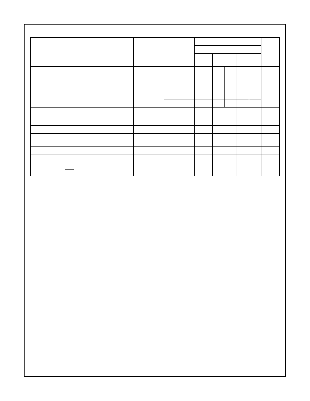
Functional Block Diagram
CE
LINE
50/60Hz
XTAL IN
XTAL OUT
V
BATT
CLOCK
OUT
INT
V
DD
V
SS
OSCILLATOR
CLOCK
LOGIC
PRESCALE SECOND MINUTE HOUR
PRESCALE
SELECT
AND
INT
4
LINE
V
SYS
POR
PSE
CPUR
POWER
SENSE
CONTROL
INT STATUS
REGISTER
FREEZE
CIRCUIT
CLOCK
CONTROL
REGISTER
INTERRUPT
CONTROL
REGISTER
CLOCK
SELECT
SECOND
LATCH
32 X 8
RAM
AM - PM AND
HOUR LOGIC
COMPARATOR
MINUTE
LATCH
8-BIT DATA BUS
HOUR
LATCH
CALENDAR
LOGIC
DAY/DAY
OF WEEK
MONTH
CDP68HC68T1
YEAR
SCK
MISO
MOSI
SERIAL
INTERFACE
FIGURE 1. REAL TIME CLOCK FUNCTIONAL DIAGRAM
Page 5
CDP68HC68T1
0
32 RAM LOCATIONS
31
32
CLOCK/CALENDAR
50
51
13 BYTES UNUSED
63
TEST MODE
R = READABLE W = WRITABLE
$00
$1F
$20
$32
$33
$3F
$5585
32
33
34
35
36
37
38
39
40
41
42
43
44
45
46
47
48
49
50
FIGURE 2. ADDRESS MAP
SECONDS
MINUTES
HOURS
DAY OF WEEK
DATE
MONTH
YEARS
NOT USED
SEC ALARM
MIN ALARM
HRS ALARM
NOT USED
NOT USED
NOT USED
NOT USED
NOT USED
STATUS REGISTER
CONTROL REGISTER
INTERRUPT CONTROL REGISTER
R, W
R, W
R, W
R, W
R, W
R, W
R, W
R, W
R, W
$20
$21
$22
$23
$24
$25
$26
$27
$28
W
$29
W
$2A
W
$2B
$2C
$2D
$2E
$2F
$30
R
$31
$32
TABLE 1. CLOCK/CALENDAR AND ALARM DATA MODES
ADDRESS LOCATION
(H) FUNCTION DECIMAL RANGE BCD DATA RANGE
(NOTE 4)
BCD DATE EXAMPLE
20 Seconds 0-59 00-59 18
21 Minutes 0-59 00-59 49
22 Hours
12 Hour Mode
1-12 81-92 (AM)
A1-B2 (PM)
A3
(Note 5)
Hours
0-23 00-23 15
24 Hour Mode
23 Day of the Week
1-7 01-07 03
(Sunday = 1)
24 Day of the Month
1-31 01-31 29
(Date)
25 Month
1-12 01-12 10
Jan = 1, Dec = 12
26 Years 0-99 00-99 85
28 Alarm Seconds 0-59 00-59 18
29 Alarm Minutes 0-59 00-59 49
2A Alarm Hours (Note 6)
12 Hour Mode
Alarm Hours
1-12 01-12 (AM)
23
21-32 (PM)
0-23 00-23 15
24 Hour Mode
NOTES:
4. Example: 3:49:18, Tuesday. Oct. 29,1985.
5. Most significant Bit, D7, is “0” for 24 hours, and “1” for 12 hour mode. Data Bit D5 is “1” for P.M. and ‘0” for A.M. in 12 hour mode.
6. Alarm hours. Data Bit D5 is “1” for P.M. and “0” for A.M. in 12 hour mode. Data Bits D7 and D6 are DON’T CARE.
5
Page 6
CDP68HC68T1
Programmers Model - Clock Registers
NAMEWRITE/READ REGISTERSHEX ADDRESS
DB7
20
21
22
23
24
25
26
31
32
TENS 0-5
TENS 0-5
12
HR
24
XXXX
76543210
76543210
PM/AM
X
TENS 0-2
TENS 0-3
TENS 0-1
TENS 0-9
X
UNITS 0-9
UNITS 0-9
UNITS 0-9
UNITS 1-7
UNITS 0-9
UNITS 0-9
UNITS 0-9
DB0
SECONDS (00-59)
MINUTES (00-59)
DB7, 1 = 12 HR., 0 = 24 HR.
DB = 1 PM, 0 = AM
HOURS (01-12 OR 00-23
DAY OF WK (01-07) SUNDAY = 1
01-28
DATE
DAY OF MONTH
MONTH (01-12) JAN = 1
DEC = 12
YEARS (00-99)
CONTROL
INTERRUPT
29
30
31
28
29
2A
30
RAM DATA BYTE
XX
765 432 1 0
NOTE: X = Don’t care writes, X = 0 when read.
WRITE ONLY REGISTERS
TENS 0-5
TENS 0-5
PM/AM
TENS 0-2
READ ONLY REGISTERS
7654321 0
D7 D6 D5 D4 D3 D2 D1 D0
HEX ADDRESS 00-1F
UNITS 0-9
UNITS 0-9
UNITS 0-9
BIT
ALARM SECONDS (00-59)
ALARM MINUTES (00-59)
ALARM HOURS (01-12 OR 00-23)
PLUS AM/PM IN 12 HR. MODE
PM = 1, AM = 0
STATUS
6
Page 7
Functional Description
CDP68HC68T1
The SPI real-time clock consists of a clock/calendar and a
32 x 8 RAM. Communications is established via the SPI
(Serial Peripheral Interface) bus. In addition to the clock/calendar data from seconds to years, and system flexibility provided by the 32-byte RAM, the clock features computer
handshaking with an interrupt output and a separate squarewave clock output that can be one of 7 different frequencies.
An alarm circuit is available that compares the alarm latches
with the seconds, minutes and hours time counters and activates the interrupt output when they are equal. The clock is
specifically designed to aid in power-down/up applications
and offers several pins to aid the designer of battery backup
systems.
Mode Select
The voltage level that is present at the V
input pin at the
SYS
end of power-on-reset selects the device to be in the single
supply or battery backup mode.
Single-Supply Mode
If V
CLK OUT, PSE and
will be completely operational.
logic level at the V
CLK OUT, PSE and
down instruction, V
is a logic high when power-on-reset is completed,
SYS
CPUR will be enabled and the device
CPUR will be placed low if the
pin goes low. If the output signals
SYS
CPUR are disabled due to a power-
brought to a logic low and then to a
SYS
logic high will re-enable these outputs. An example of the
single-supply mode is where only one supply is available
and V
DD
, V
BATT
and V
are tied together to the supply.
SYS
Battery Backup Mode
If V
OUT, PSE and
CPUR low). This condition will be held until V
threshold (about 0.7V) above V
PSE and
operational. If V
outputs CLK OUT, PSE and
example of battery backup operation occurs if V
V
connected to the V
is a logic low at the end of power-on-reset, CLK
SYS
CPUR will be disabled (CLK OUT, PSE and
rises to a
. The outputs CLK OUT,
BATT
SYS
CPUR will then be enabled and the device will be
falls below a threshold above V
SYS
BATT
CPUR will be disabled. An
is tied to
and VDD is not connected to a supply when a battery is
DD
pin. (See Pin Functions, V
BATT
SYS
BATT
the
for
Battery Backup Operation.)
Clock/Calendar (See Figure 1 and Figure 2)
The clock/calendar portion of this device consists of a long
string of counters that is toggled by a 1Hz input. The 1Hz
input is generated by a prescaler driven by an on-board
oscillator that utilizes one of four possible external crystals or
that can be driven by an external clock source. The 1Hz trigger to the counters can also be supplied by a 50Hz or 60Hz
input source that is connected to the LINE input pin.
The time counters offer seconds, minutes and hours data in
12 hour or 24 hour format. An AM/PM indicator is available
that once set, toggles every 12 hours. The calendar counters
consist of day (day of week), date (day of month), month and
years information. Data in the counters is in BCD format.
The hours counter utilizes BCD for hour data plus bits for
12/24 hour and AM/PM. The 7 time counters are accessed
serially at addresses 20H through 26H. (See Table 1).
RAM
The real-time clock also has a static 32 x 8 RAM that is
located at addresses 00-1FH. Transmitting the address/control word with bit-5 low selects RAM access. Bits 0 through 4
select the RAM location.
Alarm
The alarm is set by accessing the three alarm latches and
loading the required data. The alarm latches consist of seconds, minutes and hours registers. When their outputs equal
the values in the seconds, minutes and hours time counters,
an interrupt is generated. The interrupt output will go low if
the alarm bit in the Interrupt Control Register is set high. The
alarm interrupt bit in the Status Register is set when the
interrupt occurs (see Pin Functions,
INT Pin). To preclude a
false interrupt when loading the time counters, the alarm
interrupt bit should be set low in the Interrupt Control Register. This procedure is not required when the alarm time is
set.
Watchdog Function (See Figure 6)
When bit 7 in the Interrupt Control Register is set high, the
Clock’s CE (chip enable) pin must be toggled at a regular
interval without a serial data transfer. If the CE is not toggled,
the clock will supply a CPU reset pulse and bit 6 in the Status Register will be set. Typical ser vice and reset times are
listed below.
50Hz 60Hz XTAL
MIN MAX MIN MAX MIN MAX
Service Time - 10ms - 8.3ms - 7.8ms
Reset Time 20 40ms 16.7 33.3ms 15.6 31.3ms
Clock Out
The value in the 3 least significant bits of the Clock Control
Register selects one of seven possible output frequencies.
(See Clock Control Register). This squarewave signal is
available at the CLK OUT pin. When Power-Down operation
is initiated, the output is set low.
Control Registers and Status Registers
The operation of the Real-Time Clock is controlled by the
Clock Control and Interrupt Control Registers. Both registers
are Read-Write Registers. Another register, the Status Register, is available to indicate the operating conditions. The
Status Register is a Read only Register.
Power Control
Power control is composed of two operations, Power Sense
and Power Down/Up. Two pins are involved in power sensing, the LINE input pin and the
INT output pin. Two additional
pins are utilized during power-down/up operation. They are
the PSE (Power Supply Enable) output pin and V
SYS
input
pin.
7
Page 8
CDP68HC68T1
XTAL IN
INT INT
V
DD
0V
XTAL OUT
LINE
CPU
CDP68HC05C16B
V
REAL-TIME CLOCK
DD
STATUS REGISTER
CDP68HC68T1
I
FIGURE 3. POWER-SENSING FUNCTIONAL DIAGRAM
FROM SYSTEM
POWER
V
SYS
I
INTERRUPT
CONTROL
REGISTER
SERIAL
INTERFACE
REAL-TIME CLOCK
CDP68HC68T1
TO SYSTEM
POWER CONTROL
PSE
CLK
OUT
CPUR
MISO
MOSI
OSC
RESET
CPU
CDP68HC05C4B
POWER
UP
POWER
SENSE
OR
ALARM
CIRCUIT
PERIODIC
INTERRUPT
SIGNAL
SERIAL
INTERFACE
REAL-TIME CLOCK
CDP68HC68T1
PSE
CPUR
CLK
OUT
INT
MISO
MOSI
FIGURE 4. POWER-DOWN FUNCTIONAL DIAGRAM FIGURE 5. POWER-UP FUNCTIONAL DIAGRAM (INITIA TED
BY INTERRUPT SIGNAL
Power Sensing (See Figure 3)
When Power Sensing is enabled (Bit 5 = 1 in Interrupt Control Register), AC transitions are sensed at the LINE input pin.
Threshold detectors determine when transitions cease. After
a delay of 2.68ms to 4.64ms, plus the external input circuit RC
time constant, an interrupt is generated and a bit is set in the
Status Register. This bit can then be sampled to see if system
power has turned back on. See PIN FUNCTIONS, LINE PIN.
The power-sense circuitry operates by sensing the lev el of the
voltage presented at the line input pin. This voltage is centered around V
threshold (about 1V) from V
and as long as it is either plus or minus a
DD
a power-sense failure will not
DD
be indicated. With an AC signal present, remaining in this
V
window longer than a minimum of 2.68ms will activate
DD
the power-sense circuit. The larger the amplitude of the AC
signal, the less time it spends in the V
likely a power failure will be detected. A 60Hz, 10V
window, and the less
DD
P-P
sinewave voltage is an applicable signal to present at the LINE
input pin to setup the power sense function.
Power Down (See Figure 4)
Power down is a processor-directed operation. A bit is set in
the Interrupt Control Register to initiate operation. 3 pins are
affected. The PSE (Power Supply Enable) output, normally
high, is placed low. The CLK OUT is placed low. The
CPUR
output, connected to the processors reset input is also
placed low. In addition, the Serial Interface is disabled.
Power Up (See Figure 5 and Figure 6)
Two conditions will terminate the Power-Down mode. The
first condition (See Figure 5) requires an interrupt. The interrupt can be generated by the alarm circuit, the programmable periodic interrupt signal, or the power sense circuit.
The second condition that releases Power Down occurs
when the level on the V
level at the V
V
(See Figure 6) in the Battery Backup Mode or V
BATT
input, after previously falling to the level of
BATT
pin rises about 0.7V above the
SYS
falls to logic low and returns high in the Single Supply Mode.
8
SYS
Page 9

CDP68HC68T1
V
SS
The negative power-supply pin that is connected to ground.
V
BATT
V
SYS
SERIAL
INTERFACE
REAL-TIME CLOCK
CDP68HC68T1
FIGURE 6. POWER-UP FUNCTIONAL DIAGRAM (INITIATED BY
A RISE IN VOLTAGE ON THE “V
PSE
CPUR
CLK
OUT
SYS
MISO
MOSI
” PIN)
CLK OUT
Clock output pin. One of seven frequencies can be selected
(or this output can be set low) by the levels of the three
LSB’s in the Clock-Control Register. If a frequency is
selected, it will toggle with a 50% duty cycle except 2Hz in
the 50Hz time base mode. (Ex, if 1Hz is selected, the output
will be high for 500ms and low for the same period). During
power-down operation (bit 6 in Interrupt Control Register set
to “1”), the clock-output pin will be set low.
CPUR
CPU reset output pin. This pin functions as an N-Channel
only, open-drain output and requires an external pull-up
resistor.
INT
Interrupt output pin. This output is driven from a single NFET
pulldown transistor and must be tied to an external pull-up
resistor. The output is activated to a low level when:
1. Power-sense operation is selected (B5 = 1 in Interrupt
Control Register) and a power failure occurs.
2. A previously set alarm time occurs. The alarm bit in the
Status Register and interrupt-out signal are delayed
30.5µs when 32kHz operation is selected and 15.3µs for
2MHz and 7.6µs for 4MHz.
3. A previously selected periodic interrupt signal activates.
The Status Register must be read to set the Interrupt output
high after the selected periodic interval occurs. This is also
true when conditions 1 and 2 activate the interrupt. If power
down had been previously selected, the interrupt will also
reset the power-down functions.
PSE
Power-supply enable output pin. This pin is used to control
power to the system. The pin is set high when:
1. V
rises above the V
SYS
voltage after V
BATT
SYS
was
placed low by a system failure.
2. An interrupt occurs.
3. A power-on reset (if V
is a logic high).
SYS
The PSE pin is set low by writing a high into bit 6 (powerdown bit) in the Interrupt Control Register.
POR
Power-on reset. A Schmitt-trigger input that generates a
power-on internal reset signal using an external R-C network. Both control registers and frequency dividers for the
oscillator and line input are reset. The Status Register is
reset except for the first time up bit (B4), which is set.
Single supply or battery backup operation is selected at the
end of POR.
LINE
This input is used for two functions. When not used it
should be connected to V
via a 10kΩ resistor. The first
DD
function utilizes the input signal as the frequency source for
the timekeeping counters. This function is selected by
setting bit 6 in the Clock Control Register. The second
function enables the line input to sense a power failure.
Threshold detectors operating above and below V
DD
sense
an AC voltage loss. Bit 5 must be set to “1” in the Interrupt
Control Register and crystal or external clock source
operation is required. Bit 6 in the Clock Control Register
must be low to select XTAL operation.
Oscillator Circuit
The CDP68HC68T1 has an on-board 150K resistor that is
switched in series with its internal inverter when 32kHz is
selected via the Clock Control Register. Note: When first
powered up the series resistor is not part of the oscillator
circuit. (The CDP68HC68T1 sets up for a 4MHz oscillator).
SCK, MOSI, MISO
See Serial Peripheral Interface (SPI) section in this data sheet.
CE
A positive chip-enable input. A low level at this input holds the
serial interface logic in a reset state. This pin is also used for
the watchdog function.
9
Page 10

CDP68HC68T1
R (NOTE 8)
5 - 30pF
C1
CRYSTAL
10 - 40pF
XTAL
IN
T1
NOTES:
7. All frequencies recommended oscillator circuit. C1, C2 values
crystal dependent.
8. R used for 32KHz operation only. 100K - 300K range as specified
by crystal manufacturer.
FIGURE 7. OSCILLATOR CIRCUIT
V
SYS
22M
XTAL
OUT
C2
This input is connected to the system voltage. After the CPU
initiates power down by setting bit 6 in the Interrupt Control
Register to “1”, the level on this pin will terminate power
down if it rises about 0.7V above the level at the V
pin after previously falling below V
+0.7V. When power
BATT
BATT
input
down is terminated, the PSE pin will return high and the
Clock Output will be enabled. The
CPUR output pin will also
return high. The logic level present at this pin at the end of
POR determines the CDP68HC68T1’s operating mode.
V
BATT
The oscillator power source. The positive terminal of the battery should be connected to this pin. When the level on the
V
pin falls below V
SYS
internally connected to the V
V
rises a threshold above (0.7V) the voltage on V
SYS
the connection from V
the “LINE” input is used as the frequency source, V
be tied to V
V
BATT
or VSS. The “XTAL IN” pin must be at VSS if
DD
is at VSS. If V
IN” pin can be tied to V
+0.7V, the V
BATT
BATT
BATT
SS
pin. When the voltage on
DD
to the VDDpin is opened. When
is connected to VDD, the “XTAL
or VDD.
pin will be
BATT
BATT
BATT
may
XTAL IN, XTAL OUT
These pins are connected to a 32,768Hz. 1.048576MHz,
2.097152MHz or 4.194304MHz crystal. If an external clock
is used, it should be connected to “XTAL IN” with ‘XTAL
OUT” left open.
V
DD
The positive power-supply pin.
Clock Control Register
START-STOP
A high written into this bit will enable the counter stages of
the clock circuitry. A low will hold all bits reset in the divider
chain from 32Hz to 1Hz. A clock out selected by bits 0, 1 and
2 will not be affected by the stop function e xcept the 1Hz and
2Hz outputs.
LlNE-XTAL
When this bit is set high, clock operation will use the 50 or
60-cycle input present at the LINE input pin. When the bit is
low, the crystal input will generate the 1Hz time update.
XTAL Select
One of 4 possible crystals is selected by value in these two
bits:
0 = 4.194304MHz 2 = 1.048576MHz
1 = 2.097152MHz 3 = 32,768Hz
50-60Hz
50Hz is selected as the line input frequency when this bit is
set high. A low will select 60Hz. The power-sense bit in the
Interrupt Control Register must be set low for line frequency
operation.
Clock Out
The three bits specify one of the 7 frequencies to be used as
the squarewave clock output:
0 = XTAL 4 = Disable (low output)
1 = XTAL/2 5 = 1Hz
2 = XTAL/4 6 = 2Hz
3 = XTAL/8 7 = 50Hz or 60Hz
,
All bits are reset by a power-on reset. Therefore, the XTAL is
XTAL Operation = 64Hz
selected as the clock output at this time.
Interrupt Control Register
Watchdog
When this bit is set high, the watchdog operation will be
enabled. This function requires the CPU to toggle the CE pin
periodically without a serial-transfer requirement. In the
event this does not occur, a CPU reset will be issued. Status
Register must be read before re-enabling watchdog.
Power Down
A high in this location will initiate a power down. A CPU reset
will occur, the CLK OUT and PSE output pins will be set low
and the serial interface will be disabled.
CLOCK CONTROL REGISTER (Write/Read) - Address 31H
D7 D6 D5 D4 D3 D2 D1 D0
START LINE XTAL XTAL 50Hz CLK OUT CLK OUT CLK OUT
SEL SEL
STOP XTAL 1 0 60Hz 2 1 0
10
Page 11

CDP68HC68T1
Power Sense
This bit is used to enable the line input pin to sense a power
failure. It is set high for this function. When power sense is
selected, the input to the 50Hz to 60Hz prescaler is disconnected. Therefore, crystal operation is required when power
sense is enabled. An interrupt is generated when a power
failure is sensed and the power sense and Interrupt True bit
in the Status Register are set. When power sense is activated, a “0” must be written to this location followed by a “1”
to re-enable power sense.
The output of the alarm comparator is enabled when this bit
is set high. When a comparison occurs between the seconds, minutes and hours time and alarm counters, the interrupt output is activated. When loading the time counters, this
bit should be set low to avoid a false interrupt. This is not
required when loading the alarm counters. See Pin Functions,
INT for explanation of alarm delay.
Periodic Select
The value in these 4 bits will select the frequency of the periodic output. (See Table 2).
Alarm
INTERRUPT CONTROL REGISTER (Write/Read) - Address 32H
D7 D6 D5 D4 D3 D2 D1 D0
WATCHDOG POWER
DOWN
NOTE: All bits are reset by power-on reset.
D0 - D3 VALUE
0 Disable
1 2048Hz X
2 1024Hz X
3 512Hz X
4 256Hz X
5 128Hz X
6 64Hz X
7 32Hz X
8 16Hz X
9 8Hz X
10 4Hz X
11 2Hz X X
12 1Hz X X
13 Minute X X
14 Hour X X
15 Day X X
POWER
SENSE
TABLE 2. PERIODIC INTERRUPT OUTPUT
PERIODIC INTERRUPT
OUTPUT FREQUENCY
50 or 60Hz X
ALARM
PERIODIC SELECT
FREQUENCY TIME BASE
XTAL LINE
11
Page 12

CDP68HC68T1
STATUS REGISTER (Read Only) - Address 30H
D7 D6 D5 D4 D3 D2 D1 D0
0 WATCHDOG TEST
MODE
MODE
DISABLE
RESET
WRITE H CPOL = 1
READ H CPOL = 1
NOTES:
9. When interfacing to CDP68HC05 microcontrollers, serial clock phase bit, CPHA, must be set = 1 in the microcomputer’s Control Register.
10. MISO remains at a high Z until 8-bits of data are ready to be shifted out during a READ. It remains at a high Z during the entire WRITE
cycle.
CE SCK (Note 9) MOSI MISO
L INPUT DISABLED INPUT DISABLED HIGH Z
FIRST
TIME
UP
TRUTH TABLE
CPOL = 0
CPOL = 0
INTERRUPT
TRUE
SIGNAL
POWER
SENSE
INTERRUPT
DATA BIT LATCH HIGH Z
X NEXT DATA BIT
ALARM
INTERRUPT
CLOCK
INTERRUPT
SHIFTED OUT
(Note 10)
WATCHDOG
If this bit is set high, the watchdog circuit has detected a
CPU failure.
TEST MODE
When this bit is set high, the device is in the TEST MODE.
FIRST-TIME UP
Power-on reset sets this bit high. This signifies that data in
the RAM and Clock is not valid and should be initialized.
INTERRUPT TRUE
A high in this bit signifies that one of the three interrupts
(Power Sense, Alarm, and Clock) is valid.
POWER-SENSE INTERRUPT
This bit set high signifies that the power-sense circuit has
generated an interrupt.
ALARM INTERRUPT
When the seconds, minutes and hours time and alarm
counter are equal, this bit will be set high. Status Register
must be read before loading Interrupt Control Register for
valid alarm indication after alarm activates.
CLOCK INTERRUPT
A periodic interrupt will set this bit high.
All bits are reset by a power-on reset except the “FIRST-
TIME UP” which is set. All bits except the power-sense bit
are reset after a read of this register.
Pin Signal Description
SCK (Serial Clock Input, Note 11)
This input causes serial data to be latched from the MOSI
input and shifted out on the MISO output.
MOSI (Master Out/Slave In, Note 11)
Data bytes are shifted in at this pin, most significant bit
(MSB) first.
MISO (Master In/Slave Out)
Data bytes are shifted out at this pin, most significant bit
(MSB) first.
CE (Chip Enable, Note 12)
A positive chip-enable input. A low level at this input holds
the serial interface logic in a reset state, and disables the
output driver at the MISO pin.
NOTES:
11. These inputs will retain their previous state if the line driving
them goes into a High-Z state.
12. The CE input has as internal pull down device, if the input is in a
low state before going to High Z, the input can be left in a High Z.
Functional Description
The Serial Peripheral Interface (SPI) utilized by the
CDP68HC68T1 is a serial synchronous bus for address and
data transfers. The clock, which is generated by the microcomputer is active only during address and data transfers. In
systems using the CDP68HC05C4 or CDP68HC05D2, the
12
Page 13

CDP68HC68T1
inactive clock polarity is determined by the CPOL bit in the
microcomputer’s Control Register. A unique feature of the
CDP68HC68T1 is that it automatically determines the level
of the inactive clock by sampling SCK when CE becomes
active (see Figure 8). Input data (MOSI) is latched internally
on the internal strobe edge and output data (MISO) is shifted
out on the shift edge, as defined by Figure 8. There is one
clock for each data bit transferred (address, as well as data
bits are transferred in groups of 8).
CE
CPOL = 1
SCK
CE
CPOL = 0
SCK
MOSI MSB MSB -1
NOTE: “CPOL” is a bit that is set in the microcomputer’s Control
Register.
FIGURE 8. SERIAL RAM CLOCK (SCK) AS A FUNCTION OF
MCU CLOCK POLARITY (CPOL)
SHIFT
SHIFT
INTERNAL
STROBE
INTERNAL
STROBE
Address And Data Format
There are three types of serial transfer:
1. Address Control - Figure 9.
2. READ or WRITE Data - Figure 10.
3. Watchdog Reset (actually a non-transfer) Figure 11.
The Address/Control and Data bytes are shifted MSB first,
Into the serial data input (MOSI) and out of the serial data
output (MISO).
Any transfer of data requires an Address/Control byte to
specify a Write or Read operation and to select a Clock or
RAM location, followed by one or more bytes of data.
Data is transferred out of MISO for a Read and into MOSI for
a Write operation.
Address/Control Byte - Figure 9
It is always the first byte received after CE goes true. To
transmit a new address, CE must first go false and then true
again. Bit 5 is used to select between Clock and RAM locations.
BIT 7 6 5 4 3 2 1 0
R 0 CLK RAM A4 A3 A2 A1 A0
W/
04 A0-A4 Selects 5-Bit HEX Address of RAM or specifies Clock Register. Most Significant Address
5 CLK RAM
60
7 W/R
CE
SCK (NOTE)
RMOSI
NOTE: SCK can be either polarity.
FIGURE 9. ADDRESS/CONTROL BYTE-TRANSFER WAVEFORMS
Bit. If equal to “1”, A0 through A4 selects a Clock Register. If equal to “0”, A0 through A4
selects one of 32 RAM locations. Must be set to ”0” when not in Test Mode 7W/R W/R = “1”
initiates one or more WRITE cycles.W/R = “0”, initiates one or more READ cycles.
CLOCK
0W/
RAM
A2
A1 A0A3A4
13
Page 14

Read/Write Data (See Figure 10)
Read/Write data follows the Address/Control byte.
76543210BIT
D7 D6 D5 D4 D3 D2 D1 D0
CE
SCK (NOTE)
CDP68HC68T1
MOSI
MISO
NOTE: SCK can be either polarity.
FIGURE 10. READ/WRITE DATA TRANSFER WAVEFORMS
Watchdog Reset - (See Figure 11)
When watchdog operation is selected, CE must be toggled
periodically or a CPU reset will be outputted.
SERVICE
TIME
CE
SCK
CPUR
FIGURE 11. WATCHDOG OPERATION WAVEFORMS
SERVICE
TIME
D2
D2
D1 D0D3D4D5D6D7
D1 D0D3D4D5D6D7
Address And Data
Data transfers can occur one byte at a time (Figure 12) or in
a multibyte burst mode (Figure 13). After the Real-Time
Clock enabled, an Address/Control word is sent to set the
CLOCK or RAM and select the type of operation (i.e., Read
or Write). For a single-byte Read or Write, one byte is transferred to or from the Clock Register or RAM location specified in the Address/Control byte and the Real-Time Clock is
then disabled. Write cycle causes the latched Clock Register
or RAM address to automatically increment. Incrementing
continues after each transfer until the device is disabled.
After incrementing to 1FH the address will “wrap” to 00H and
continue. Therefore, when the RAM is selected the address
will “wrap” to 00H and when the clock is selected the
address will “wrap” 20H.
14
Page 15

CE
SCK
CDP68HC68T1
READ
WRITE
CE
SCK
MOSI
MOSIWRITE
MOSI
MISO
ADDRESS BYTE WRITE DATA
ADDRESS BYTE
READ DATA
FIGURE 12. SINGLE-BYTE TRANSFER WAVEFORMS
DATA BYTEADDRESS BYTE
DATA BYTE
DATA BYTE
READ
MOSI
MISO
W/
R ADDRESS
ADDRESS BYTE
DATA BYTEDATA BYTEDATA BYTE
DATA BYTE
DATA BYTE +1
DATA BYTE + (n-1)
FIGURE 13. MULTIPLE-BYTE TRANSFER WAVEFORMS
15
Page 16

CDP68HC68T1
Dynamic Electrical Specifications Bus Timing V
IDENT. NO PARAMETER
1 Chip Enable Setup Time t
2 Chip Enable After Clock Hold Time t
3 Clock Width High t
4 Clock Width Low t
5 Data In to Clock Setup Time t
7 Clock to Data Propagation Delay t
8 Chip Disable to Output High Z t
11 Output Rise Time t
12 Output Fall Time t
A Data in After Clock Hold Time t
B Clock to Data Out Active t
C Clock Recovery Time t
±10%, VSS = 0VDC, TA = 40oC to 85oC
DD
LIMITS (ALL TYPES)
VDD = 3.3V VDD = 5V
MIN MAX MIN MAX
EVCV
CVEX
WH
WL
DVCV
CVDV
EXQZ
r
f
CVDX
CVQX
REC
200 - 100 - ns
250 - 125 - ns
400 - 200 - ns
400 - 200 - ns
200 - 100 - ns
- 200 - 100 ns
- 200 - 100 ns
- 200 - 100 ns
- 200 - 100 ns
200 - 100 - ns
- 200 - 100 ns
200 - 200 - ns
UNITS
16
Page 17

Timing Diagrams
CDP68HC68T1
5 A 5
MOSI
CE
SCK
MOSI
MISO
CE
SCK
W/R
I
A6
34
A0
D7
D6OD1
O
C
DO
N
N
2
FIGURE 14. WRITE-CYCLE TIMING WAVEFORMS
A5
W/R
A6 A0
D7
D6ODI
O
7 8
DO
N
2CI
12118
N
4 3
FIGURE 15. READ-CYCLE TIMING WAVEFORMS
System Diagrams
AC
LINE
NOTE: Example of a system in which power is always on. Clock circuit driven by line input frequency.
BRIDGE
REGULATOR
FIGURE 16. POWER-ON ALWAYS SYSTEM DIAGRAM
PORV
DD
INT
V
LINE
CDP68HC68T1
V
BATT
XTAL IN
SYS
CPUR
CE
SCK
MOSI
MISO
V
DD
IRQ
V
DD
CDP68HC05C8B
RESET
PORT
SCK
MOSI
MISO
17
Page 18

CDP68HC68T1
System Diagrams
AC
LINE
(Continued)
BRIDGE
GENERATOR
V
CDP68HC68T1
LINE
V
DD
BATT
V
DD
POR
V
SYS
INT
CPUR
CLK OUT
CE
MISO
MOSI
SCK
V
DD
IRQ
CDP68HC05C8B
RESET
OSC 1
PORT (e.g., PCO)
MISO
MOSI
SCK
V
DD
NOTE: Example of a system in which the power is controlled by an external source. The LINE input pin can sense when the switch opens by use
of the POWER-SENSE INTERRUPT. The CDP68HC68T1 crystal drives the clock input to the CPU using the CLK OUT pin. On power down when
V
SYS
< V
BATT
+ 0.7V. V
will power the CDP68HC68T1. A threshold detect activates a P-Channel switch, connecting V
BATT
BATT
to VDD. V
BATT
always supplies power to the oscillator, keeping voltage frequency variation to a minimum.
FIGURE 17. EXTERNALLY CONTROLLED POWER SYSTEM DIAGRAM
A Procedure for P o wer-Do wn Operation might consist of the following:
1. Set power sense operation b y writing bit 5 high in the Interrupt Control Register .
2. When an interrupt occurs, the CPU reads the Status Register to determine the interrupt source.
3. Sensing a power f ailure , the CPU does the necessary housekeeping to prepare f or shutdown.
4. The CPU reads the Status Register again after sev eral milliseconds to determine validity of po w er f ailure .
5. The CPU sets power-down bit 6 and disables all interrupts in the Interrupt Control Register when power down is verified. This
causes the CPU reset and clock out to be held low and disconnects the serial interface.
6. When power returns and V
rises above V
SYS
, power down is terminated. The CPU reset is released and serial communi-
BATT
cation is established.
18
Page 19

CDP68HC68T1
System Diagrams
0.047
20k
AC
LINE
1k
RTC
V
DD
REGULATOR
CHARGE
(Continued)
R
0.1
22M
100k
POR V
V
BATT
XTAL
LINE
DDVSYS
CPUR
V
SS
PSE
INT
CLK
OUT
CE
SPI
NC
(EPS)
ENABLED
POWER
SUPPLY
V
DD
V
DD
3
RESET
CDP68HC05C4B
IRQ
OSC1
PORT
SPI
V
SS
FIGURE 18. EXAMPLE OF A SYSTEM WITH A BATTERY BACKUP
19
Page 20

CDP68HC68T1
System Diagrams
CLOCK BUTTON
IGNITION
5V
REG
+
12V
-
(Continued)
LINE V
V
BATT
POR
XTAL
2MHz
DD
T1
V
SS
V
SYS
PSE
CPUR
CLK OUT
INT
SPI
CE
ENABLED POWER
V
DD
PORT
RESET
CDP68HC05C4B
OSC1
IRQ
3
SPI
PORT
V
SS
Example of an automotive system. The V
and LINE inputs can be used to sense the ignition turning on and off. An external
SYS
switch is included to activate the system without turning on the ignition. Also, the CMOS CPU is not po wered down with the system
V
, but is held in a low power reset mode during power down. When restoring power the CDP68HC68T1 will enable the CLK
DD
OUT pin and set the PSE and
CPUR high.
Important Application Note: Those units with a code of 6PG have delayed alarm interrupts of 8.3ms regardless of
CDP68HC68T1’s operating frequency. (See Pin Functions, INT.) In addition, reading the Status Register before delayed alarm activates will disable alarm signal.
FIGURE 19. AUTOMOTIVE SYSTEM DIAGRAM
20
Page 21

Dual-In-Line Plastic Packages (PDIP)
CDP68HC68T1
E
C
L
e
A
C
e
B
BASE
PLANE
SEATING
PLANE
D1
B1
D
A2
A1
A
L
e
C
S
-C-
D1
e
B
0.010 (0.25) C AMB
NOTES:
1. Controlling Dimensions: INCH. In case of conflict between English and
Metric dimensions, the inch dimensions control.
2. Dimensioning and tolerancing per ANSI Y14.5M-1982.
3. Symbols are defined in the “MO Series Symbol List” in Section 2.2 of
Publication No. 95.
4. Dimensions A, A1 and L are measured with the package seated in JEDEC seating plane gauge GS-3.
5. D, D1, and E1 dimensions do not include mold flash or protrusions.
Mold flash or protrusions shall not exceed 0.010 inch (0.25mm).
6. E and are measured with the leads constrained to be perpendic-
e
A
ular to datum .
-C-
7. eB and eC are measured at the lead tips with the leads unconstrained.
eC must be zero or greater.
8. B1 maximum dimensions do not include dambar protrusions. Dambar
protrusions shall not exceed 0.010 inch (0.25mm).
9. N is the maximum number of terminal positions.
10. Corner leads (1, N, N/2 and N/2 + 1) for E8.3, E16.3, E18.3, E28.3,
E42.6 will have a B1 dimension of 0.030 - 0.045 inch (0.76 - 1.14mm).
E16.3 (JEDEC MS-001-BB ISSUE D)
16 LEAD DUAL-IN-LINE PLASTIC PACKAGE
INCHES MILLIMETERS
SYMBOL
A - 0.210 - 5.33 4
A1 0.015 - 0.39 - 4
A2 0.115 0.195 2.93 4.95 -
B 0.014 0.022 0.356 0.558 B1 0.045 0.070 1.15 1.77 8, 10
C 0.008 0.014 0.204 0.355 -
D 0.735 0.775 18.66 19.68 5
D1 0.005 - 0.13 - 5
E 0.300 0.325 7.62 8.25 6
E1 0.240 0.280 6.10 7.11 5
e 0.100 BSC 2.54 BSC -
e
A
e
B
0.300 BSC 7.62 BSC 6
- 0.430 - 10.92 7
L 0.115 0.150 2.93 3.81 4
N16 169
NOTESMIN MAX MIN MAX
Rev. 0 12/93
21
Page 22

CDP68HC68T1
Ceramic Dual-In-Line Metal Seal Packages (SBDIP)
LEAD FINISH
c1
bbb C A - B
BASE
PLANE
SEATING
PLANE
S1
b2
b
ccc C A - BMD
S
-A-
-B-
D
A
A
S S
e
S S
D
-D-
E
S2
-C-
BASE
METAL
M
SECTION A-A
Q
A
L
eA/2
aaa C A - B
M
b1
M
(b)
eA
S S
c
D
NOTES:
1. Index area: A notch or a pin one identification mark shall be located adjacent to pin one and shall be located within the shaded
area shown. The manufacturer’s identification shall not be used
as a pin one identification mark.
2. The maximum limits of lead dimensions b and c or M shall be
measured at the centroid of the finished lead surfaces, when
solder dip or tin plate lead finish is applied.
3. Dimensions b1 and c1 apply to lead base metal only. Dimension
M applies to lead plating and finish thickness.
4. Corner leads (1, N, N/2, a nd N/2+1) may be configured with a
partial lead paddle. For this configuration dimension b3 replaces
dimension b2.
5. Dimension Q shall be measured from the seating plane to the
base plane.
6. Measure dimension S1 at all four corners.
7. Measure dimension S2 from the top of the ceramic body to the
nearest metallization or lead.
8. N is the maximum number of terminal positions.
9. Braze fillets shall be concave.
10. Dimensioning and tolerancing per ANSI Y14.5M - 1982.
11. Controlling dimension: INCH.
D16.3 MIL-STD-1835 CDIP2-T16 (D-2, CONFIGURATION C)
16 LEAD CERAMIC DUAL-IN-LINE METAL SEAL PACKAGE
(c)
SYMBOL
A - 0.200 - 5.08 -
b 0.014 0.026 0.36 0.66 2
b1 0.014 0.023 0.36 0.58 3
b2 0.045 0.065 1.14 1.65 b3 0.023 0.045 0.58 1.14 4
c 0.008 0.018 0.20 0.46 2
c1 0.008 0.015 0.20 0.38 3
D - 0.840 - 21.34 -
E 0.220 0.310 5.59 7.87 -
e 0.100 BSC 2.54 BSC eA 0.300 BSC 7.62 BSC -
eA/2 0.150 BSC 3.81 BSC -
L 0.125 0.200 3.18 5.08 -
Q 0.015 0.060 0.38 1.52 5
S1 0.005 - 0.13 - 6
S2 0.005 - 0.13 - 7
α
aaa - 0.015 - 0.38 bbb - 0.030 - 0.76 -
ccc - 0.010 - 0.25 -
M - 0.0015 - 0.038 2
N16 168
INCHES MILLIMETERS
90
o
105
o
90
o
105
NOTESMIN MAX MIN MAX
o
Rev. 0 4/94
-
22
Page 23

CDP68HC68T1
6
4
Small Outline Plastic Packages (SOIC)
N
INDEX
AREA
123
-A-
0.25(0.010) B
E
SEATING PLANE
D
-C-
H
-B-
A
M
L
h x 45
M
o
α
e
B
0.25(0.010) C AMB
M
NOTES:
1. Symbols are defined in the “MO Series Symbol List” in Section 2.2 of
Publication Number 95.
2. Dimensioning and tolerancing per ANSI Y14.5M-1982.
3. Dimension “D” does not include mold flash, protrusions or gate burrs.
Mold flash, protrusion and gate burrs shall not exceed 0.15mm (0.00
inch) per side.
4. Dimension “E” does not include interlead flash or protrusions. Interlead
flash and protrusions shall not exceed 0.25mm (0.010 inch) per side.
5. The chamfer on the body is optional. If it is not present, a visual index
feature must be located within the crosshatched area.
6. “L” is the length of terminal for soldering to a substrate.
7. “N” is the number of terminal positions.
8. Terminal numbers are shown for reference only.
9. The lead width “B”, as measured 0.36mm (0.014 inch) or greater above
the seating plane, shall not exceed a maximum value of 0.61mm (0.02
inch)
10. Controlling dimension: MILLIMETER. Converted inch dimensions are
not necessarily exact.
A1
0.10(0.004)
S
C
M16.3 (JEDEC MS-013-AA ISSUE C)
16 LEAD WIDE BODY SMALL OUTLINE PLASTIC PACKAGE
INCHES MILLIMETERS
SYMBOL
A 0.0926 0.1043 2.35 2.65 -
A1 0.0040 0.0118 0.10 0.30 -
B 0.013 0.0200 0.33 0.51 9
C 0.0091 0.0125 0.23 0.32 D 0.3977 0.4133 10.10 10.50 3
E 0.2914 0.2992 7.40 7.60 4
e 0.050 BSC 1.27 BSC -
H 0.394 0.419 10.00 10.65 -
h 0.010 0.029 0.25 0.75 5
L 0.016 0.050 0.40 1.27 6
N16 167
o
α
0
o
8
o
0
o
8
Rev. 0 12/93
NOTESMIN MAX MIN MAX
-
23
Page 24

CDP68HC68T1
Small Outline Plastic Packages (SOIC)
N
INDEX
AREA
123
-A-
0.25(0.010) B
E
SEATING PLANE
D
-C-
H
-B-
A
M
L
h x 45
M
o
α
e
B
0.25(0.010) C AMB
M
NOTES:
1. Symbols are defined in the “MO Series Symbol List” in Section 2.2 of
Publication Number 95.
2. Dimensioning and tolerancing per ANSI Y14.5M-1982.
3. Dimension “D” does not include mold flash, protrusions or gate burrs.
Mold flash, protrusion and gate burrs shall not exceed 0.15mm (0.006
inch) per side.
4. Dimension “E” does not include interlead flash or protrusions. Interlead
flash and protrusions shall not exceed 0.25mm (0.010 inch) per side.
5. The chamfer on the body is optional. If it is not present, a visual index
feature must be located within the crosshatched area.
6. “L” is the length of terminal for soldering to a substrate.
7. “N” is the number of terminal positions.
8. Terminal numbers are shown for reference only.
9. The lead width “B”, as measured 0.36mm (0.014 inch) or greater
above the seating plane, shall not exceed a maximum value of
0.61mm (0.024 inch)
10. Controlling dimension: MILLIMETER. Converted inch dimensions
are not necessarily exact.
A1
0.10(0.004)
S
C
M20.3 (JEDEC MS-013-AC ISSUE C)
20 LEAD WIDE BODY SMALL OUTLINE PLASTIC PACKAGE
INCHES MILLIMETERS
SYMBOL
A 0.0926 0.1043 2.35 2.65 -
A1 0.0040 0.0118 0.10 0.30 -
B 0.013 0.0200 0.33 0.51 9
C 0.0091 0.0125 0.23 0.32 D 0.4961 0.5118 12.60 13.00 3
E 0.2914 0.2992 7.40 7.60 4
e 0.050 BSC 1.27 BSC -
H 0.394 0.419 10.00 10.65 -
h 0.010 0.029 0.25 0.75 5
L 0.016 0.050 0.40 1.27 6
N20 207
o
α
0
o
8
o
0
o
8
Rev. 0 12/93
NOTESMIN MAX MIN MAX
-
All Intersil semiconductor products are manufactured, assembled and tested under ISO9000 quality systems certification.
Intersil products are sold by description only. Intersil Corporation reserves the right to make changes in circuit design and/or specifications at any time without
notice. Accordingly, the reader is cautioned to verify that data sheets are current before placing orders. Information furnished by Intersil is believed to be accurate
and reliable. However, no responsibility is assumed by Intersil or its subsidiaries for its use; nor for any infringements of patents or other rights of third parties which
may result from its use. No license is granted by implication or otherwise under an y patent or patent rights of Intersil or its subsidiaries.
For information regarding Intersil Corporation and its products, see web site http://www.intersil.com
Sales Office Headquarters
NORTH AMERICA
Intersil Corporation
P. O. Box 883, Mail Stop 53-204
Melbourne, FL 32902
TEL: (407) 724-7000
FAX: (407) 724-7240
EUROPE
Intersil SA
Mercure Center
100, Rue de la Fusee
1130 Brussels, Belgium
TEL: (32) 2.724.2111
FAX: (32) 2.724.22.05
ASIA
Intersil (Taiwan) Ltd.
Taiwan Limited
7F-6, No. 101 Fu Hsing North Road
Taipei, Taiwan
Republic of China
TEL: (886) 2 2716 9310
FAX: (886) 2 2715 3029
24
 Loading...