

Page 1
CDP6872
January 1996
Features
• Single Supply Operation at 32kHz . . . . . . . 2.0V to 7.0V
• Operating Frequency Range. . . . . . . . 10kHz to 10MHz
• Supply Current at 32kHz . . . . . . . . . . . . . . . . . . . . . .5µA
• Supply Current at 1MHz . . . . . . . . . . . . . . . . . . . .130µA
• Drives 2 CMOS Loads
• Only Requires an External Crystal for Operation
Applications
• Battery Powered Circuits
• Remote Metering
• Embedded Microprocessors
• Palm Top/Notebook PC
Low Power Crystal Oscillator
Description
The CDP6872 is a very low power crystal-controlled oscillators
that can be externally programmed to operate between 10kHz
and 10MHz. For normal operation it requires only the addition
of a crystal. The part exhibits very high stability over a wide
operating voltage and temperature range.
The CDP6872 also features a disable mode that switches
the output to a high impedance state. This feature is useful
for minimizing power dissipation during standby and when
multiple oscillator circuits are employed.
Ordering Information
PART
NUMBER
CDP6872E -40
CDP6872M -40
CDP6872H -40
TEMPERATURE
RANGE PACKAGE
o
C to +85oC 8 Lead Plastic DIP
o
C to +85oC 8 Lead Plastic SOIC (N)
o
C to +85oC DIE
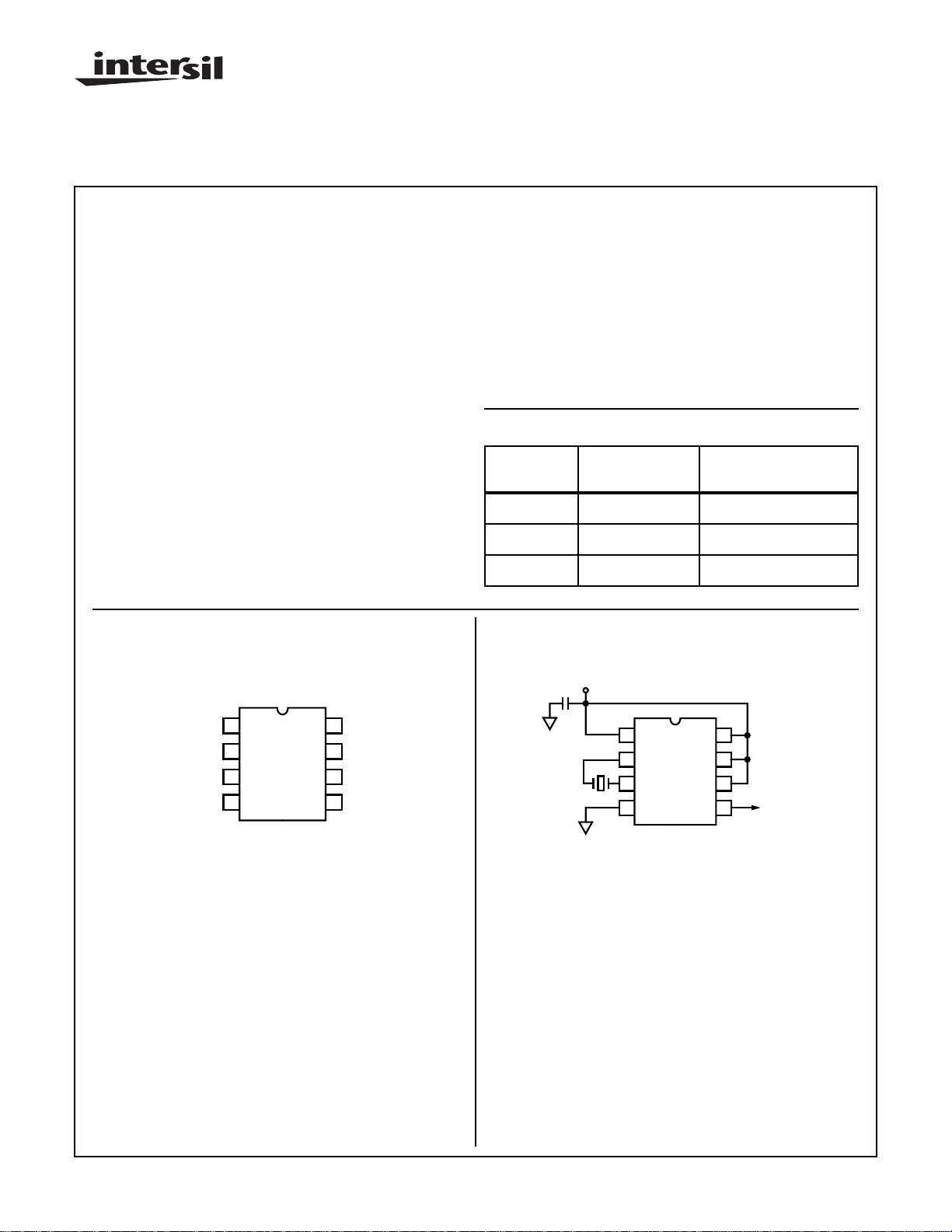
Pinout
V
DD
OSC IN
OSC OUT
V
SS
CDP6872 (PDIP, SOIC)
TOP VIEW
1
2
3
4
8
7
6
5
ENABLE
FREQ 2
FREQ 1
OUTPUT
Typical Application Circuit
V
DD
0.1µf
1
2
32.768kHz
CRYSTAL
32.768kHz MICROPOWER CLOCK OSCILLATOR
CDP6872
3
4
8
7
6
32.768kHz
5
CLOCK
CAUTION: These devices are sensitive to electrostatic discharge; follow proper IC Handling Procedures.
http://www.intersil.com or 407-727-9207
| Copyright © Intersil Corporation 1999
1
File Number 4069
Page 2
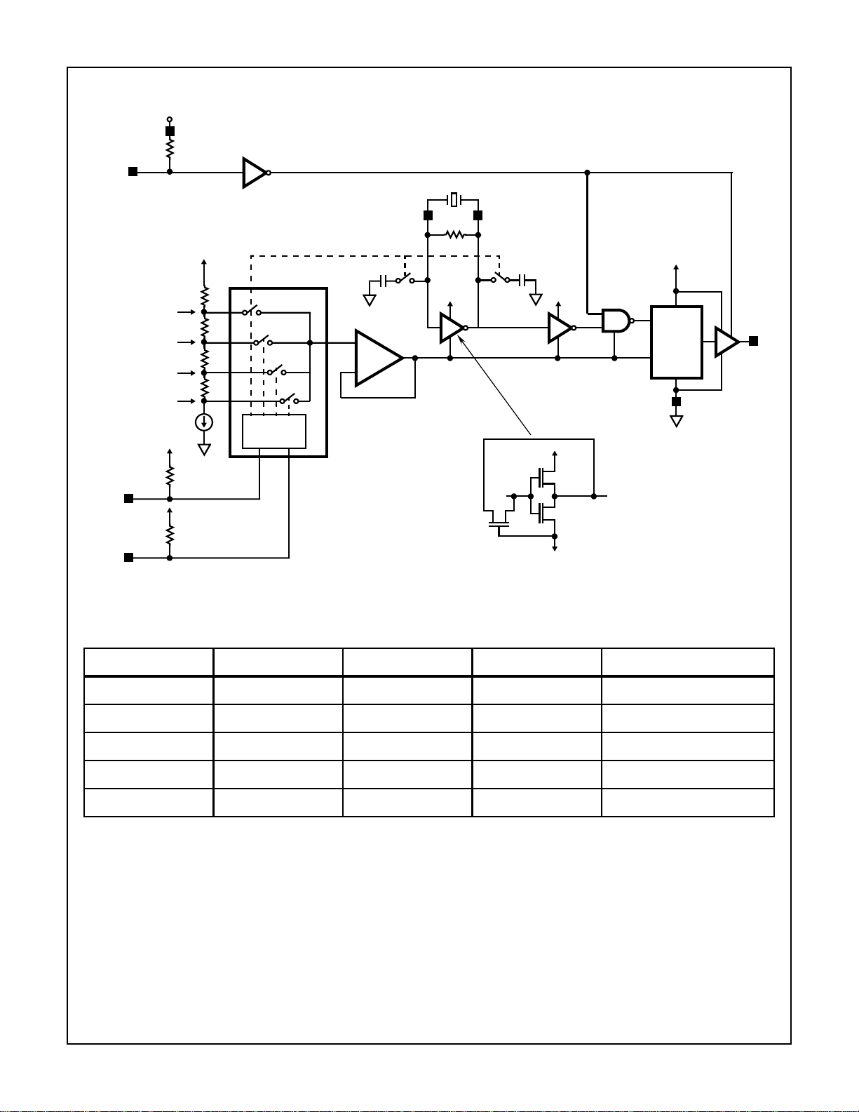
Simplified Block Diagram
V
DD
(NOTE 1)
1
8
ENABLE
CDP6872
EXTERNAL CRYSTAL
FREQ 1
FREQ 2
VDD - 1.4V
VDD - 2.2V
VDD - 3.0V
VDD - 3.8V
V
DD
6
V
DD
7
I
BIAS
V
DD
(NOTE 1)
(NOTE 1)
S1a
S2
1 OF 4
DECODE
S3
S4
15pF
V
RN
+
-
BUFFER AMP
OSC IN 2 3 OSC OUT
S1b S1c
R
F
15pF
V
DD
IN
P
R
F
OSCILLATOR
V
DD
V
DD
LEVEL
SHIFTER
V
RN
4
V
SS
V
DD
P
OUT
N
V
RN
OUTPUT
5
BUFFER
FREQUENCY SELECTION TRUTH TABLE
ENABLE FREQ 1 FREQ 2 SWITCH OUTPUT RANGE
1 1 1 S1a, b, c 10kHz - 100kHz
1 1 0 S2 100kHz - 1MHz
1 0 1 S3 1MHz - 5MHz
1 0 0 S4 5MHz - 10MHz+
0 X X X High Impedance
NOTE:
1. Logic input pull-up resistors are constant current source of 0.4µA.
2
Page 3
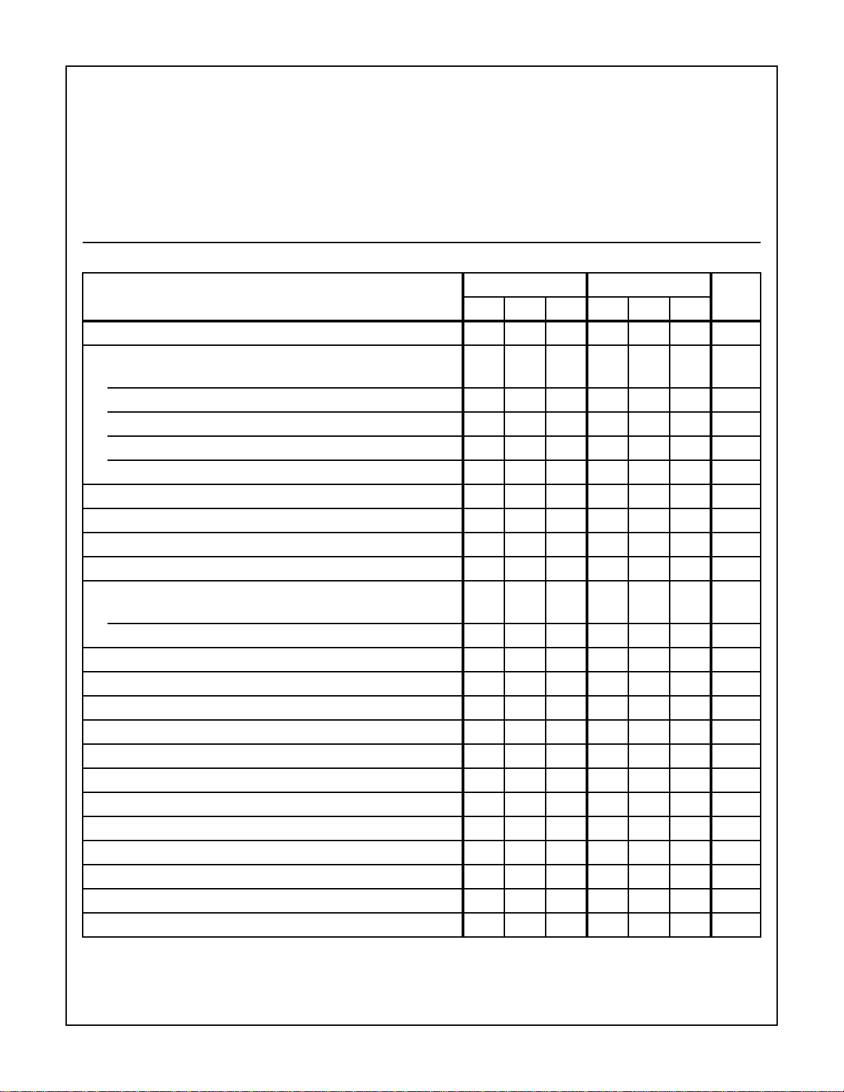
Specifications CDP6872
Absolute Maximum Ratings Operating Conditions
Supply Voltage . . . . . . . . . . . . . . . . . . . . . . . . . . . . . . . . . . . . .10.0V
Voltage (any pin). . . . . . . . . . . . . . . . . . . . . . .VSS-0.3V to VDD+0.3V
Junction Temperature (Plastic Package) . . . . . . . . . . . . . . . +150oC
ESD Rating (Note 2). . . . . . . . . . . . . . . . . . . . . . . . . . . . . . . >4000V
Lead Temperature (Soldering 10s). . . . . . . . . . . . . . . . . . . . +300oC
(SOIC - Lead Tip Only)
CAUTION: Stresses above those listed in “Absolute Maximum Ratings” may cause permanent damage to the device. This is a stress only rating and operation
of the device at these or any other conditions above those indicated in the operational sections of this specification is not implied.
Operating Temperature (Note 3) . . . . . . . . . . . . . . . .-40oC to +85oC
Storage Temperature Range. . . . . . . . . . . . . . . . . .-65oC to +150oC
Thermal Information (Typical)
Thermal Resistance (oC/W) θ
8 Lead Plastic DIP. . . . . . . . . . . . . . . . . . . . . . . . . . . . 125
8 Lead Plastic SOIC . . . . . . . . . . . . . . . . . . . . . . . . . . 170
JA
Electrical Specifications V
= GND, TA = +25oC, Unless Otherwise Specified
SS
VDD= 5V VDD = 3V
PARAMETER
VDD Supply Range (f
= 32kHz) 2 5 7 - - - V
OSC
IDD Supply Current
f
= 32kHz, EN = 0 Standby - 5.0 9.0 - - - µA
OSC
f
= 32kHz, CL = 10pF (Note 1), EN = 1, Freq1 = 1, Freq2 = 1 - 5.2 10.2 - 3.6 6.1 µA
OSC
f
= 32kHz, CL = 40pF, EN = 1, Freq1 = 1, Freq2 = 1 - 10 15 - 6.5 9 µA
OSC
f
= 1MHz, CL = 10pF (Note 1), EN = 1, Freq1 = 0, Freq2 = 1 - 130 200 - 90 180 µA
OSC
f
= 1MHz, CL = 40pF, EN = 1, Freq1 = 0, Freq2 = 1 - 270 350 - 180 270 µA
OSC
VOH Output High Voltage (I
VOL Output Low Voltage (I
IOH Output High Current (V
IOL Output Low Current (V
= -1mA) 4.0 4.9 - - 2.8 - V
OUT
= 1mA) - 0.07 0.4 - 0.1 - V
OUT
≥ 4V) - -10 -5 - - - mA
OUT
≤ 0.4V) 5.0 10.0 ----mA
OUT
Three-State Leakage Current
(V
= 0V, 5V, TA = 25oC, -40oC) -0.1----nA
OUT
(V
= 0V, 5V, TA = 85oC) -10----nA
OUT
IIN Enable, Freq1, Freq2 Input Current (VIN = VSS to VDD) - 0.4 1.0 - - - µA
UNITSMIN TYP MAX MIN TYP MAX
VIH Input High Voltage Enable, Freq1, Freq2 2.0 ----- V
VIL Input Low Voltage Enable, Freq1, Freq2 - - 0.8 - - - V
Enable Time (CL = 18pF, RL = 1kΩ) -800----ns
Disable Time (CL = 18pF, RL = 1kΩ) -90----ns
tR Output Rise Time (10% - 90%, f
tF Output Fall Time (10% - 90%, f
Duty Cycle (CL = 40pF) f
Duty Cycle (CL = 40pF) f
= 1MHz, Packaged Part Only (Note 4) 40 54 60 - - - %
OSC
= 32kHz, (See Typical Curves) - 41 - - 44 - %
OSC
Frequency Stability vs. Supply Voltage (f
Frequency Stability vs. Temperature (f
Frequency Stability vs. Load (f
= 32kHz, CL = 40pF) - 12 25 - 12 - ns
OSC
= 32kHz, CL = 40pF) - 12 25 - 14 - ns
OSC
= 32kHz, VDD = 5V, CL=10pF) - 1 ----ppm/V
OSC
= 32kHz, VDD = 5V, CL=10pF) - 0.1 ----ppm/oC
OSC
= 32kHz, VDD = 5V, CL=10pF) - 0.01 ----ppm/pF
OSC
NOTES:
1. Calculated using the equation IDD = IDD (No Load) + (VDD) (f
OSC
)(CL)
2. Human body model.
3. This product is production tested at +25oC only.
4. Duty cycle will vary with supply voltage, oscillation frequency, and parasitic capacitance on the crystal pins.
3
Page 4
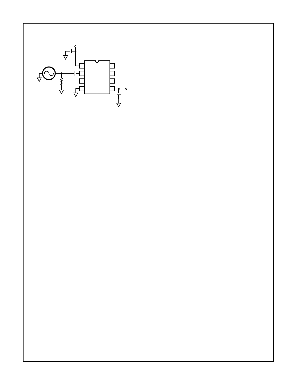
CDP6872
Test Circuits
+5V
0.1µF
1V
P-P
50Ω
1000pF
1
2
CDP6872
3
4
FIGURE 1.
ENABLE
8
FREQ 2
7
FREQ 1
6
5
C
L
18pF
V
OUT
In production the CDP6872 is tested with a 32kHz and a
1MHz crystal. However for characterization purposes data
was taken using a sinewave generator as the frequency
determining element, as shown in Figure 1. The 1V
P-P
input
is a smaller amplitude than what a typical crystal would generate so the transitions are slower. In general the Generator
data will show a “worst case” number for I
, duty cycle, and
DD
rise/fall time. The Generator test method is useful for testing
a variety of frequencies quickly and provides curves which
can be used for understanding performance trends. Data for
the CDP6872 using crystals has also been taken. This data
has been overlaid onto the generator data to provide a reference for comparison.
Theory of Operation
The CDP6872 is a Pierce Oscillator optimized for low power
consumption, requiring no external components except for a
bypass capacitor and a Parallel Mode Crystal. The Simplified Block Diagram shows the Crystal attached to pins 2 and
3, the Oscillator input and output. The crystal drive circuitry
is detailed showing the simple CMOS inverter stage and the
P-channel device being used as biasing resistor R
inverter will operate mostly in its linear region increasing the
amplitude of the oscillation until limited by its transconductance and voltage rails, V
biasing using R
to center the oscillating waveform at the
F
and VRN. The inverter is self
DD
input threshold. Do not interfere with this bias function with
external loads or excessive leakage on pin 2. Nominal value
for R
is 17MΩ in the lowest frequency range to 7MΩ in the
F
highest frequency range.
The CDP6872 optimizes its power for 4 frequency ranges
selected by digital inputs Freq1 and Freq2 as shown in the
Block Diagram. Internal pull up resistors (constant current
0.4µA) on Enable, Freq1 and Freq2 allow the user simply to
leave one or all digital inputs not connected for a corresponding “1” state. All digital inputs may be left open for
10kHz to 100kHz operation.
A current source develops 4 selectable reference voltages
through series resistors. The selected voltage, V
ered and used as the negative supply rail for the oscillator
, is buff-
RN
. The
F
section of the circuit. The use of a current source in the reference string allows for wide supply variation with minimal
effect on performance. The reduced operating voltage of the
oscillator section reduces power consumption and limits
transconductance and bandwidth to the frequency range
selected. For frequencies at the edge of a range, the higher
range may provide better performance.
The OSC OUT waveform on pin 3 is squared up through a
series of inverters to the output drive stage. The Enable
function is implemented with a NAND gate in the inverter
string, gating the signal to the level shifter and output stage.
Also during Disable the output is set to a high impedance
state useful for minimizing power during standby and when
multiple oscillators are OR'd to a single node.
Design Considerations
The low power CMOS transistors are designed to consume
power mostly during transitions. Keeping these transitions
short requires a good decoupling capacitor as close as possible to the supply pins 1 and 4. A ceramic 0.1µF is recommended. Additional supply decoupling on the circuit board
with 1µF to 10µF will further reduce overshoot, ringing and
power consumption. The CDP6872, when compared to a
crystal and inverter alone, will speed clock transition times,
reducing power consumption of all CMOS circuitry run from
that clock.
Power consumption may be further reduced by minimizing
the capacitance on moving nodes. The majority of the power
will be used in the output stage driving the load. Minimizing
the load and parasitic capacitance on the output, pin 5, will
play the major role in minimizing supply current. A secondary
source of wasted supply current is parasitic or crystal load
capacitance on pins 2 and 3. The CDP6872 is designed to
work with most available crystals in its frequency range with
no external components required. Two 15pF capacitors are
internally switched onto crystal pins 2 and 3 to compensate
the oscillator in the 10kHz to 100kHz frequency range.
The supply current of the CDP6872 may be approximately
calculated from the equation:
I
= IDD(Disabled) + VDD × F
DD
where: IDD = Total supply current
V
= Total voltage from VDD (pin1) to VSS (pin4)
DD
F
= Frequency of Oscillation
OSC
C
= Output (pin5) load capacitance
L
Example #1:
= 5V, F
V
DD
I
(Disabled) = 4.5µA (Figure 10)
DD
I
= 4.5µA + (5V)(100kHz)(30pF) = 19.5µA
DD
Measured I
= 100kHz, CL = 30pF
OSC
= 20.3µA
DD
Example #2:
= 5V, F
V
DD
I
(Disabled) = 75µA (Figure 9)
DD
I
= 75µA + (5V)(5MHz)(30pF) = 825µA
DD
Measured I
= 5MHz, CL = 30pF
OSC
= 809µA
DD
OSC
× C
L
4
Page 5
CDP6872
Crystal Selection
For general purpose applications, a Parallel Mode Crystal is
a good choice for use with the CDP6872. However for
applications where a precision frequency is required, the
designer needs to consider other factors.
Crystals are available in two types or modes of oscillation,
Series and Parallel. Series Mode crystals are manufactured
to operate at a specified frequency with zero load capacitance and appear as a near resistive impedance when oscillating. Parallel Mode crystals are manufactured to operate
with a specific capacitive load in series, causing the crystal
to operate at a more inductive impedance to cancel the load
capacitor. Loading a crystal with a different capacitance will
“pull” the frequency off its value.
The CDP6872 has 4 operating frequency ranges. The higher
three ranges do not add any loading capacitance to the
oscillator circuit. The lowest range, 10kHz to 100kHz, automatically switches in two 15pF capacitors onto OSC IN and
OSC OUT to eliminate potential start-up problems. These
capacitors create an effective crystal loading capacitor equal
to the series combination of these two capacitors. For the
CDP6872, in the lowest range, the effective loading capacitance is 7.5pF. Therefore the choice for a crystal, in this
range, should be a Parallel Mode crystal that requires a
7.5pF load.
In the higher 3 frequency ranges, the capacitance on OSC
IN and OSC OUT will be determined by package and layout
parasitics, typically 4 to 5pF. Ideally the choice for crystal
should be a Parallel Mode set for 2.5pF load. A crystal manufactured for a different load will be “pulled” from its nominal
frequency (see Crystal Pullability).
+5V
C
1
C
2
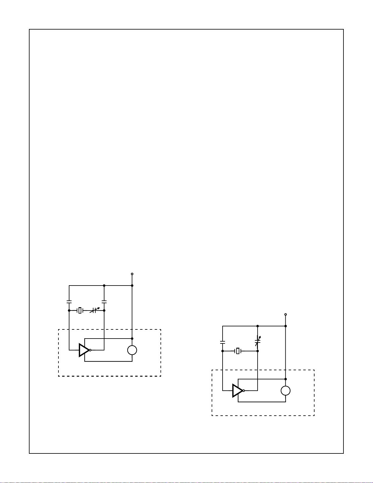
Frequency Fine Tuning
Two Methods will be discussed for fine adjustment of the
crystal frequency. The first and preferred method (Figure 2),
provides better frequency accuracy and oscillator stability
than method two (Figure 3). Method one also eliminates
start-up problems sometimes encountered with 32kHz tuning fork crystals.
For best oscillator performance, two conditions must be met:
the capacitive load must be matched to both the inverter and
crystal to provide ideal conditions for oscillation, and the frequency of the oscillator must be adjustable to the desired
frequency. In Method two these two goals can be at odds
with each other; either the oscillator is trimmed to frequency
by de-tuning the load circuit, or stability is increased at the
expense of absolute frequency accuracy.
Method one allows these two conditions to be met independently. The two fixed capacitors, C
mum load to the oscillator and crystal. C
frequency at which the circuit oscillates without appreciably
changing the load (and thus the stability) of the system.
Once a value for C
has been determined for the particular
3
type of crystal being used, it could be replaced with a fixed
capacitor. For the most precise control over oscillator frequency, C
should remain adjustable.
3
This three capacitor tuning method will be more accurate
and stable than method two and is recommended for 32kHz
tuning fork crystals; without it they may leap into an overtone
mode when power is initially applied.
Method two has been used for many years and may be preferred in applications where cost or space is critical. Note
that in both cases the crystal loading capacitors are connected between the oscillator and V
AC ground. The Simplified Block Diagram shows that the
oscillating inverter does not directly connect to V
erenced to V
and VRN. Therefore VDD is the best AC
DD
ground available.
and C2, provide the opti-
1
; do not use VSS as an
DD
adjusts the
3
but is ref-
SS
XTAL C
2
OSC IN
3
3
OSC OUT
CDP6872
FIGURE 2.
+5V
1
V
DD
+
VREG
-
C
1
2
OSC IN
XTAL
C
2
3
OSC OUT
CDP6872
FIGURE 3.
1
V
DD
+
VREG
-
5
Page 6

CDP6872
Typical values of the capacitors in Figure 2 are shown below.
Some trial and error may be required before the best combination is determined. The values listed are total capacitance
including parasitic or other sources. Remember that in the
10kHz to 100kHz frequency range setting the CDP6872
switches in two internal 15pF capacitors.
CRYSTAL
FREQUENCY
32kHz 33pF 5-50pF
1MHz 33pF 5-50pF
2MHz 25pF 5-50pF
4MHz 22pF 5-100pF
LOAD CAPS
C1, C2
TRIMMER CAP
C3
Crystal Pullability
Figure 4 shows the basic equivalent circuit for a crystal and
its loading circuit.
V
DD
C
1
C
2
OSC IN
M
R
L
M
M
C
0
C
2
3
OSC OUT
Layout Considerations
Due to the extremely low current (and therefore high impedance) the circuit board layout of the CDP6872 must be given
special attention. Stray capacitance should be minimized.
Keep the oscillator traces on a single layer of the PCB. Avoid
putting a ground plane above or below this layer. The traces
between the crystal, the capacitors, and the OSC pins
should be as short as possible. Completely surround the
oscillator components with a thick trace of V
to minimize
DD
coupling with any digital signals. The final assembly must be
free from contaminants such as solder flux, moisture, or any
other potential source of leakage. A good solder mask will
help keep the traces free of moisture and contamination over
time.
Further Reading
Al Little “HA7210 Low Power Oscillator: Micropower Clock
Oscillator and Op Amps Provide System Shutdown for
Battery Circuits”. Intersil Application Note AN9317.
Robert Rood “Improving Start-Up Time at 32KHz for the
HA7210 Low Power Crystal Oscillator”. Intersil Application
Note AN9334.
S. S. Eaton “Timekeeping Advances Through COS/MOS
Technology”. Intersil Application Note ICAN-6086.
E. A. Vittoz et. al. “High-Performance Crystal Oscillator circuits: Theory and Application”. IEEE Journal of Solid-State
Circuits, Vol. 23, No3, June 1988, pp774-783.
M. A. Unkrich et. al. “Conditions for Start-Up in Crystal Oscillators”. IEEE Journal of Solid-State Circuits, Vol. 17, No1,
Feb. 1982, pp87-90.
FIGURE 4.
Where: CM = Motional Capacitance
L
= Motional Inductance
M
R
= Motional Resistance
M
C
= Shunt Capacitance
0
1
C
----------------------------- Equivalent Crystal Load==
CL
1
-------
C
1
-------+
C
1
2
If loading capacitance is connected to a Series Mode Crystal, the new Parallel Mode frequency of resonance may be
calculated with the following equation:
C
F
FS1
P
M
------------------------------------ -+=
2C0CCL+
Where: FP = Parallel Mode Resonant Frequency
F
= Series Mode Resonant Frequency
S
In a similar way, the Series Mode resonant frequency may
be calculated from a Parallel Mode crystal and then you may
calculate how much the frequency will “pull” with a new load.
Marvin E. Frerking “Crystal Oscillator Design and Temperature Compensation”. New York: Van Nostrand-Reinhold,
1978. Pierce Oscillators Discussed pp56-75.
6
Page 7

Die Characteristics
DIE DIMENSIONS:
68 x 64 x 14 ± 1mils
METALLIZATION:
Type: Si - Al
Thickness: 10k
GLASSIVATION:
Type: Nitride (Si
Silox Thickness: 7k
Nitride Thickness: 8kÅ ± 1kÅ
DIE ATTACH:
Material: Silver Epoxy - Plastic DIP and SOIC
Å ± 1kÅ
) Over Silox (SiO2, 3% Phos)
3N4
Å ± 1kÅ
CDP6872
SUBSTRATE POTENTIAL: V
SS
Metallization Mask Layout
CRYSTAL (2)
CRYSTAL (3)
CDP6872
DD
(1) V
(8) ENABLE
(7) FREQ 2
(6) FREQ 1
(4)
SS
V
OUTPUT (5)
7
Page 8

Typical Performance Curves
CDP6872
CL = 40pF, F
= 5MHz, VDD = 5V, VSS = GND
OSC
1.0V/DIV. 20.0ns/DIV.
= 18pF, F
C
L
= 5MHz, VDD = 5V, VSS = GND
OSC
1.0V/DIV. 20.0ns/DIV.
FIGURE 5. OUTPUT WAVEFORM (CL = 40pF) FIGURE 6. OUTPUT WAVEFORM (CL = 18pF)
1050
FIN = 5MHz, EN = 1, F1 = 0, F2 = 0, CL = 30pF, VCC = 5V
1000
950
GENERATOR† (1V
900
P-P
)
26
EN = 1, F1 = 1, F2 = 1, FIN = 100kHz, CL = 30pF, VCC = 5V
25
24
GENERATOR† (1V
23
22
P-P
)
850
SUPPLY CURRENT (µA)
800
750
-100 -50 0 50 100 150
TEMPERATURE (oC)
X
TAL
AT +25oC
21
SUPPLY CURRENT (µA)
20
19
18
-100 -50 0 50 100 150
X
AT +25oC
TAL
TEMPERATURE (oC)
FIGURE 7. SUPPLY CURRENT vs TEMPERATURE FIGURE 8. SUPPLY CURRENT vs TEMPERATURE
350
FIN = 5MHz, EN = 0, F1 = 0, F2 = 0, VCC = 5V
300
250
200
150
SUPPLY CURRENT (µA)
100
50
0
-100 -50 0 50 100 150
TEMPERATURE (oC)
GENERATOR† (1V
X
AT +25oC
TAL
P-P
)
7.5
EN = 0, F1 = 1, F2 = 1, FIN= 100kHz, VCC = 5V
7
6.5
6
5.5
5
SUPPLY CURRENT (µA)
4.5
4
-100 -50 0 50 100 150
X
TEMPERATURE (oC)
GENERATOR† (1V
AT +25oC
TAL
P-P
)
FIGURE 9. DISABLE SUPPLY CURRENT vs TEMPERATURE FIGURE 10. DISABLE SUPPLY CURRENT vs TEMPERATURE
†Refer to Test Circuit (Figure 1).
8
Page 9

CDP6872
Typical Performance Curves
3000
EN = 1, F1 = 0, F2 = 0, CL = 18pF, GENERATOR† (1V
2500
VCC = +8V
2000
1500
1000
SUPPLY CURRENT (µA)
500
0
4567891011
FREQUENCY (MHz)
(Continued)
VCC = +5V
P-P
1400
)
EN = 1, F1 = 0, F2 =1, CL = 18pF, GENERATOR† (1V
1200
1000
800
600
400
SUPPLY CURRENT (µA)
200
0
0123456
VCC = +8V
FREQUENCY (MHz)
FIGURE 11. SUPPLY CURRENT vs FREQUENCY FIGURE 12. SUPPLY CURRENT vs FREQUENCY
300
EN = 1, F1 = 1, F2 = 0, CL = 18pF, GENERATOR† (1V
250
VCC = +8V
200
VCC = +5V
150
100
SUPPLY CURRENT (µA)
50
0
0 100 200 300 400 500 600 700 800 900 1000 1100
FREQUENCY (kHz)
VCC = +3V
P-P
)
50
EN = 1, F1 = 0, F2 =1, CL = 18pF, GENERATOR† (1V
40
30
20
SUPPLY CURRENT (µA)
10
0
0 102030405060708090100110
FREQUENCY (kHz)
VCC = +5V
FIGURE 13. SUPPLY CURRENT vs FREQUENCY FIGURE 14. SUPPLY CURRENT vs FREQUENCY
VCC = +5V
VCC = +3V
VCC = +8V
P-P
VCC = +3V
P-P
)
)
EN = 0, F1 = 0, F2 = 0, CL = 18pF, GENERATOR† (1V
250
200
150
100
SUPPLY CURRENT (µA)
50
0
4567891011
FREQUENCY (MHz)
)
P-P
VCC = +8V
VCC = +5V
VCC = +3V
EN = 0, F1 = 0, F2 = 1, CL = 18pF, GENERATOR† (1V
120
110
100
90
80
70
60
SUPPLY CURRENT (µA)
50
40
30
0123456
FREQUENCY (MHz)
VCC = +8V
VCC = +5V
VCC = +3V
P-P
)
FIGURE 15. DISABLED SUPPLY CURRENT vs FREQUENCY FIGURE 16. DISABLE SUPPLY CURRENT vs FREQUENCY
†Refer to Test Circuit (Figure 1).
9
Page 10

CDP6872
Typical Performance Curves
EN = 0, F1 = 1, F2 = 0, CL = 18pF, GENERATOR† (1V
35
30
25
20
15
SUPPLY CURRENT (µA)
10
5
0 100 200 300 400 500 600 700 800 900 1000 1100
FREQUENCY (kHz)
(Continued)
P-P
VCC = +8V
VCC = +5V
VCC = +3V
)
EN = 0, F1 = 1, F2 = 1, CL = 18pF, GENERATOR† (1V
11
10
9
8
7
6
5
SUPPLY CURRENT (µA)
4
3
2
0 102030405060708090100110
FREQUENCY (kHz)
P-P
VCC = +8V
VCC = +5V
VCC = +3V
FIGURE 17. DISABLE SUPPLY CURRENT vs FREQUENCY FIGURE 18. DISABLE SUPPLY CURRENT vs FREQUENCY
EN = 1, F1 = 0, F2 = 0, VCC = +5V, GENERATOR† (1V
3000
2500
2000
CL = 40pF
P-P
)
EN = 1, F1 = 0, F2 = 1, VCC = +5V, GENERATOR† (1V
1400
1200
1000
800
P-P
CL = 40pF
)
)
1500
CL = 18pF
SUPPLY CURRENT (µA)
1000
500
4567891011
FREQUENCY (MHz)
600
400
SUPPLY CURRENT (µA)
200
0
0123456
FREQUENCY (MHz)
FIGURE 19. SUPPLY CURRENT vs FREQUENCY FIGURE 20. SUPPLY CURRENT vs FREQUENCY
EN = 1, F1 = 1, F2 = 0, VCC = +5V, GENERATOR† (1V
300
CL = 40pF
250
200
150
CL = 18pF
100
SUPPLY CURRENT (µA)
50
0
0 100 200 300 400 500 600 700 800 900 1000 1100
FREQUENCY (kHz)
P-P
)
EN = 1, F1 = 1, F2 = 1, VCC = +5V, GENERATOR† (1V
35
30
25
20
15
10
SUPPLY CURRENT (µA)
5
0
0 102030405060708090100110
FREQUENCY (kHz)
FIGURE 21. SUPPLY CURRENT vs FREQUENCY FIGURE 22. SUPPLY CURRENT vs FREQUENCY
CL = 18pF
P-P
CL = 40pF
CL = 18pF
)
†Refer to Test Circuit (Figure 1).
10
Page 11

CDP6872
Typical Performance Curves
FIN = 5MHz, F1 = 0, F2 = 0, CL = 30pF, VCC = 5V
60
55
50
45
DUTY CYCLE (%)
40
35
30
-100 -50 0 50 100 150
GENERATOR† (1V
TEMPERATURE (
(Continued)
o
C)
X
TAL
FIGURE 23. DUTY CYCLE vs TEMPERATURE FIGURE 24. DUTY CYCLE vs TEMPERATURE
F1 = F2 = 0, V
70
DATA COLLECTED USING CRYSTALS
AT EACH FREQUENCY
65
60
55
DUTY CYCLE (%)
50
F1 = 0, F2 = 0 RECOMMENDED FOR 5MHz TO 10MHz RANGE
45
0
= 5V, CL = 18pF, C1 = C2 = 0
DD
FREQUENCY (MHz)
15 20510
FIGURE 25. DUTY CYCLE vs FREQUENCY FIGURE 26. DUTY CYCLE vs FREQUENCY
AT +25oC
)
P-P
FIN = 100kHz, F1 = 1, F2 = 1, CL = 30pF, VCC = 5V
70
GENERATOR†(1V
60
50
40
DUTY CYCLE (%)
30
20
10
-100 -50 0 50 100 150
TEMPERATURE (
F1 = 0, F2 = 1, V
70
DATA COLLECTED USING CRYSTALS
AT EACH FREQUENCY
65
60
55
50
DUTY CYCLE (%)
45
F1 = 0, F2 = 1 RECOMMENDED FOR 1MHz TO 5MHz RANGE
40
0
= 5V, CL = 18pF, C1 = C2 = 0
DD
FREQUENCY (MHz)
P-P
)
X
AT +25oC
TAL
o
C)
7946123 5 8
F1 = 1, F2 = 0, V
65
DATA COLLECTED USING CRYSTALS
AT EACH FREQUENCY
60
55
50
DUTY CYCLE (%)
45
F1 = 1, F2 = 0 RECOMMENDED FOR 100kHz TO 1MHz RANGE
40
0
= 5V, CL = 18pF, C1 = C2 = 0
DD
1500 2000500 1000 2500 3000 3500
FREQUENCY (kHz)
FIGURE 27. DUTY CYCLE vs FREQUENCY FIGURE 28. DUTY CYCLE vs FREQUENCY
†Refer to Test Circuit (Figure 1).
47
46
45
44
43
DUTY CYCLE (%)
42
41
40
11
F1 = F2 = 1, V
DATA COLLECTED USING CRYSTALS
AT EACH FREQUENCY
0
= 5V, CL = 18pF, C1 = C2 = 0
DD
F1 = 1, F2 = 1 RECOMMENDED
FOR 10kHz TO 100kHz RANGE
FREQUENCY (kHz)
150 20050 100
Page 12

CDP6872
Typical Performance Curves
(Continued)
VCC = 5V, CL = 30pF, GENERATOR† (1V
30
25
20
15
32kHz
1MHz
5MHz
10MHz
6
5
4
FIN = 5MHz, F1 = 0, F2 = 0
10
5
3
0
-5
-10
FREQUENCY CHANGE (PPM)
-15
-20
DEVIATION FROM 5.0V FREQUENCY
24 6
SUPPLY VOLTAGE (V)
V
DD
FIGURE 29. FREQUENCY CHANGE vs V
DD
FIN = 5MHz, F1 = 0, F2 = 0, CL = 30pF, VCC = 5V
13
12
11
Tf GENERATOR† (1V
P-P
)
10
9
8
7
6
RISE/FALL TIME (ns)
5
4
Tr GENERATOR† (1V
Tf X
AT +25oC
TAL
Tr X
TAL
P-P
AT +25oC
)
3
2
-100 -50 0 50 100 150
TEMPERATURE (
o
C)
2
EDGE JITTER (% OF PERIOD)
1
0
-100 -50 0 50 100 150
FIN = 100kHz, F1 = 1, F2 = 1
TEMPERATURE (
FIGURE 30. EDGE JITTER vs TEMPERATURE
FIN = 100kHz, F1 = 1, F2 = 1, CL = 30pF, VCC = 5V
12
11
10
9
Tr GENERATOR† (1V
8
7
6
RISE/FALL TIME (ns)
5
4
3
2
-100 -50 0 50 100 150
Tf GENERATOR† (1V
)
P-P
TEMPERATURE (
FIGURE 31. RISE/FALL TIME vs TEMPERATURE FIGURE 32. RISE/FALL TIME vs TEMPERATURE
o
o
P-P
C)
Tf X
C)
)
P-P
TAL
Tr X
)
AT +25oC
AT +25oC
TAL
VCC = 5V, GENERATOR† (1V
P-P
)
30
Tf (FIN = 100kHz)
25
Tf (FIN = 5MHz)
20
Tr (FIN = 100kHz)
15
RISE/FALL TIME (ns)
10
5
10 20 30 40 50 60 70 80 90 100 110
CL (pF)
FIGURE 33. RISE/FALL TIME vs C
L
†Refer to Test Circuit (Figure 1).
(F
IN
Tr
= 5MHz)
RISE/FALL TIME (ns)
12
C
= 18pF, GENERATOR† (1V
L
P-P
)
15
14
13
12
11
10
Tf (FIN = 5MHz)
Tf (FIN= 100kHz)
Tr (FIN= 5MHz)
Tr (FIN= 100kHz)
9
8
7
6
5
4
23456789
VCC (+VOLTS)
FIGURE 34. RISE/FALL TIME vs V
CC
Page 13

CDP6872
Typical Performance Curves
VDD = 5V, VSS = GND
620
F1 = 0, F2 = 0
580
540
500
460
420
380
340
300
TRANSCONDUCTANCE (µA/V)
260
10K 100K 1M 10M
50Ω
1000pF
23
CDP6872
FREQUENCY (Hz)
436.5µA/V
1µF
100Ω
178
o
(Continued)
180
170
160
150
140
PHASE (DEGREES)
V
= 5V, VSS = GND
DD
500
F1 = 0, F2 = 1
460
420
380
340
300
260
TRANSCONDUCTANCE (µA/V)
10K 100K 1M 10M
50Ω
1000pF
23
CDP6872
FREQUENCY (Hz)
1µF
311.6µA/V
177
100Ω
o
FIGURE 35. TRANSCONDUCTANCE vs FREQUENCY FIGURE 36. TRANSCONDUCTANCE vs FREQUENCY
V
= 5V, VSS = GND
DD
240
F1 = 1, F2 = 0
220
200
180
160
140
120
100
TRANSCONDUCTANCE (µA/V)
10K 100K 1M 10M
176.6
1000pF
50Ω
156.7µA/V
o
1µF
23
CDP6872
FREQUENCY (Hz)
100Ω
FIGURE 37. TRANSCONDUCTANCE vs FREQUENCY
180
170
160
150
140
PHASE (DEGREES)
130
VDD = 5V, VSS = GND
20
F1 = 1, F2 = 1
15
10
5
0
1000pF
50Ω
TRANSCONDUCTANCE (µA/V)
10K 100K 1M
CDP6872
6.56µA/V
166
1µF
23
FREQUENCY (Hz)
o
100Ω
FIGURE 38. TRANSCONDUCTANCE vs FREQUENCY
180
170
160
150
140
PHASE (DEGREES)
130
180
170
160
150
140
130
PHASE (DEGREES)
120
110
F1 = F2 = 1, VDD = 5V, CL = 18pF, TA = 25oC, F
60
55
50
45
DUTY CYCLE (%)
40
35
0 20 40 60 80 100 120
EPSON PART #
C-001R32.768K-A
NDK PART #
MX-38
R
(kΩ)
S
OSC IN
FIGURE 39. DUTY CYCLE vs R
XTAL
2
CDP6872
at 32kHz
S
= 32.768kHz
OSC
R
S
3
OSC OUT
NOTE: Figure 39 (Duty Cycle vs RS at 32kHz) should only be used for 32kHz crystals. RS may be used at other frequencies to adjust Duty
Cycle but experimentation will be required to find an appropriate value. The RS value will be proportional to the effective series resistance of the crystal being used.
13
Page 14

Dual-In-Line Plastic Packages (PDIP)
N
D1
E1
-C-
-B-
A1
A2
A
L
e
C
S
INDEX
AREA
BASE
PLANE
SEATING
PLANE
1 2 3 N/2
-A-
D1
B1
B
D
e
0.010 (0.25) C AMB
NOTES:
1. Controlling Dimensions: INCH. In case of conflict between
English and Metric dimensions, the inch dimensions control.
2. Dimensioning and tolerancing per ANSI Y14.5M-1982.
3. Symbols are defined in the “MO Series Symbol List” in Section
2.2 of Publication No. 95.
4. Dimensions A, A1 and L are measured with the package seated
in JEDEC seating plane gauge GS-3.
5. D, D1, and E1 dimensions do not include mold flash or protrusions. Mold flash or protrusions shall not exceed 0.010 inch
(0.25mm).
6. E and are measured with the leads constrained to be per-
e
pendicular to datum .
A
-C-
7. eB and eC are measured at the lead tips with the leads unconstrained. eC must be zero or greater.
8. B1 maximum dimensions do not include dambar protrusions.
Dambar protrusions shall not exceed 0.010 inch (0.25mm).
9. N is the maximum number of terminal positions.
10. Corner leads (1, N, N/2 and N/2 + 1) for E8.3, E16.3, E18.3,
E28.3, E42.6 will have a B1 dimension of 0.030 - 0.045 inch
(0.76 - 1.14mm).
CDP6872
E
C
L
e
A
C
e
B
E8.3 (JEDEC MS-001-BA ISSUE D)
8 LEAD DUAL-IN-LINE PLASTIC PACKAGE
INCHES MILLIMETERS
SYMBOL
A - 0.210 - 5.33 4
A1 0.015 - 0.39 - 4
A2 0.115 0.195 2.93 4.95 -
B 0.014 0.022 0.356 0.558 B1 0.045 0.070 1.15 1.77 8, 10
C 0.008 0.014 0.204 0.355 -
D 0.355 0.400 9.01 10.16 5
D1 0.005 - 0.13 - 5
E 0.300 0.325 7.62 8.25 6
E1 0.240 0.280 6.10 7.11 5
e 0.100 BSC 2.54 BSC -
e
A
e
B
0.300 BSC 7.62 BSC 6
- 0.430 - 10.92 7
L 0.115 0.150 2.93 3.81 4
N8 89
NOTESMIN MAX MIN MAX
Rev. 0 12/93
14
Page 15

Small Outline Plastic Packages (SOIC)
CDP6872
N
INDEX
AREA
123
-A-
0.25(0.010) B
H
E
-B-
SEATING PLANE
D
A
-C-
M
L
h x 45
M
o
α
e
B
0.25(0.010) C AMB
M
NOTES:
1. Symbols are defined in the “MO Series Symbol List” in Section
2.2 of Publication Number 95.
2. Dimensioning and tolerancing per ANSI Y14.5M-1982.
3. Dimension “D” does not include mold flash, protrusions or gate
burrs. Mold flash, protrusion and gate burrs shall not exceed
0.15mm (0.006 inch) per side.
4. Dimension “E” does not include interlead flash or protrusions. Interlead flash and protrusions shall not exceed 0.25mm (0.010
inch) per side.
5. The chamfer on the body is optional. If it is not present, a visual
index feature must be located within the crosshatched area.
6. “L” is the length of terminal for soldering to a substrate.
7. “N” is the number of terminal positions.
8. Terminal numbers are shown for reference only.
9. The lead width “B”, as measured 0.36mm (0.014 inch) or greater
above the seating plane, shall not exceed a maximum value of
0.61mm (0.024 inch).
10. Controlling dimension: MILLIMETER. Converted inch dimensions are not necessarily exact.
A1
0.10(0.004)
S
M8.15 (JEDEC MS-012-AA ISSUE C)
8 LEAD NARROW BODY SMALL OUTLINE PLASTIC PACKAGE
INCHES MILLIMETERS
SYMBOL
A 0.0532 0.0688 1.35 1.75 -
A1 0.0040 0.0098 0.10 0.25 -
B 0.013 0.020 0.33 0.51 9
C 0.0075 0.0098 0.19 0.25 D 0.1890 0.1968 4.80 5.00 3
E 0.1497 0.1574 3.80 4.00 4
e 0.050 BSC 1.27 BSC H 0.2284 0.2440 5.80 6.20 -
C
h 0.0099 0.0196 0.25 0.50 5
L 0.016 0.050 0.40 1.27 6
N8 87
o
α
0
o
8
o
0
o
8
Rev. 0 12/93
NOTESMIN MAX MIN MAX
-
All Intersil semiconductor products are manufactured, assembled and tested under ISO9000 quality systems certification.
Intersil products are sold by description only. Intersil Corporation reserves the right to make changes in circuit design and/or specifications at any time without
notice. Accordingly, the reader is cautioned to verify that data sheets are current before placing orders. Information furnished by Intersil is believed to be accurate
and reliable. However, no responsibility is assumed by Intersil or its subsidiaries for its use; nor for any infringements of patents or other rights of third parties which
may result from its use. No license is granted by implication or otherwise under any patent or patent rights of Intersil or its subsidiaries.
For information regarding Intersil Corporation and its products, see web site http://www.intersil.com
Sales Office Headquarters
NORTH AMERICA
Intersil Corporation
P. O. Box 883, Mail Stop 53-204
Melbourne, FL 32902
TEL: (407) 724-7000
FAX: (407) 724-7240
EUROPE
Intersil SA
Mercure Center
100, Rue de la Fusee
1130 Brussels, Belgium
TEL: (32) 2.724.2111
FAX: (32) 2.724.22.05
ASIA
Intersil (Taiwan) Ltd.
Taiwan Limited
7F-6, No. 101 Fu Hsing North Road
Taipei, Taiwan
Republic of China
TEL: (886) 2 2716 9310
FAX: (886) 2 2715 3029
Spec Number
15
 Loading...