

Page 1
March 1997
CDP1881C,
CDP1882, CDP1882C
CMOS 6-Bit Latch
and Decoder Memory Interfaces
Features
• Performs Memory Address Latch and Decoder
Functions Multiplexed or Non-Multiplexed
• Decodes Up to 16K Bytes of Memory
• Interfaces Directly with CDP1800-Series Microprocessors at Maximum Clock Frequency
• Can Replace CDP1866 and CDP1867 (Upward Speed
and Function Capability)
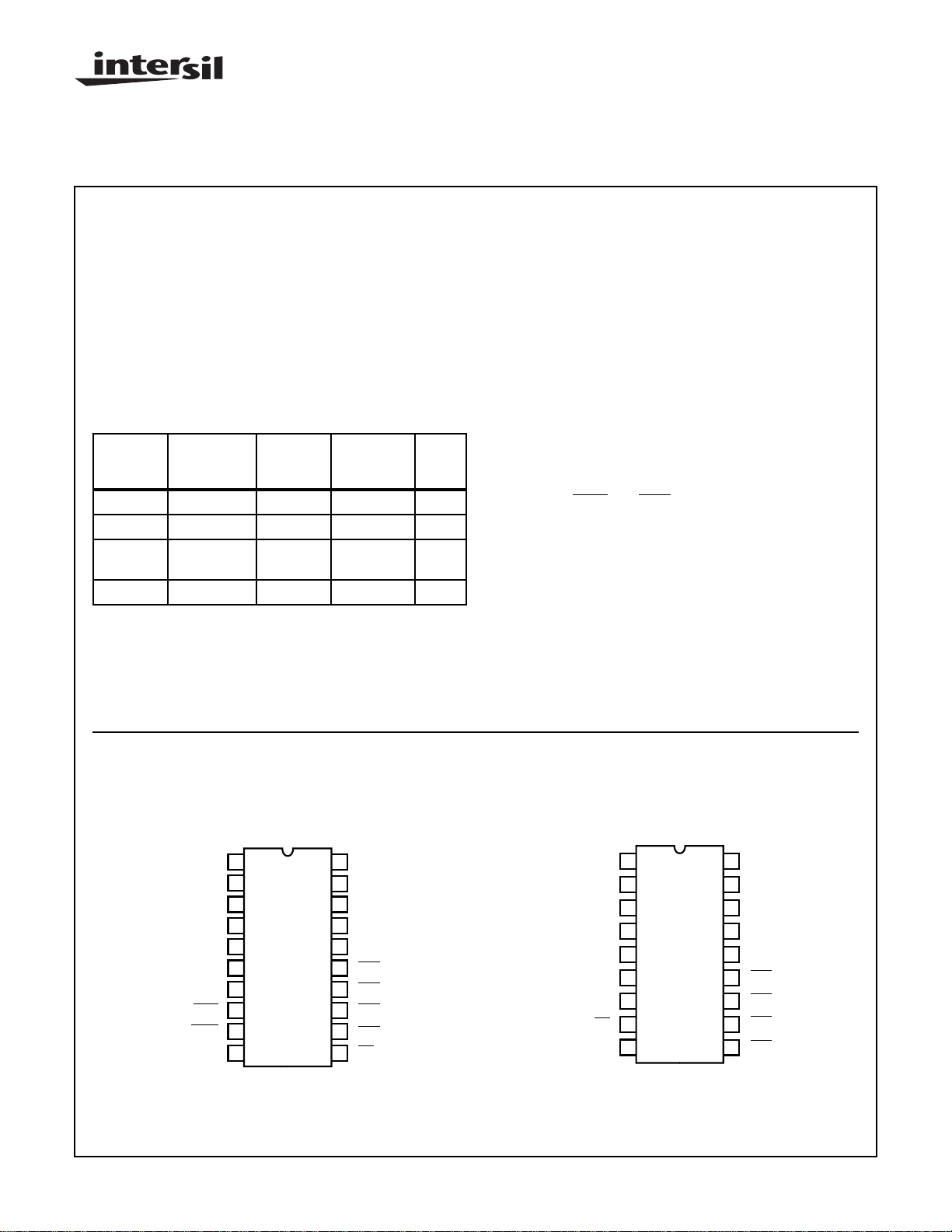
Ordering Information
TEMP.
RANGE
PACKAGE 5V 10V
PDIP CDP1881CE - -40 to +85 E20.3
PDIP CDP1882CE - -40 to +85 E18.3
PDIP
Burn-In
SBDIP - CDP1882D -40 to +85 D18.3
CDP1882CEX - -40 to +85 E18.3
(oC)
PKG.
NO.
Description
The CDP1881C, CDP1882 and CDP1882C are CMOS 6-bit
memory latch and decoder circuits intended for use in
CDP1800 series microprocessor systems. They can interface directly with the multiplexed address bus of this system
at maximum clock frequency, and up to four 4K x 8-bit memories to provide a 16K byte memory system. With four 2K x
8-bit memories an 8K byte system can be decoded.
The devices are also compatible with non-multiplexed
address bus microprocessors. By connecting the clock input
to V
, the latches are in the data-following mode and the
DD
decoded outputs can be used in general purpose memorysystem applications.
The CDP1881C, CDP1882 and CDP1882C are intended for
use with 2K or 4K byte RAMs and are identical except that in
the CDP1882
The CDP1882 is functionally identical to the CDP1882C. It
differs in that the CDP1882 has recommended operating
voltage range of 4V to 10.5V and the C version has a recommended operating voltage range of 4V to 6.5V.
The CDP1881C, CDP1882 and CDP1882C are supplied in
20 lead and 18 lead packages, respectively. The
CDP1881C is supplied only in a dual-in-line plastic package (E suffix). The CDP1882 is supplied in dual-in-line,
hermetic side-brazed ceramic (D suffix) and in plastic (E
suffix) packages.
MWR and MRD are excluded.
Pinouts
CDP1881C
(PDIP)
TOP VIEW
MA5
MA4
MA3
MA2
MA1
MA0
MRD
MWR
V
1
2
3
4
5
6
7
8
9
10
SS
| Copyright © Intersil Corporation 1999
CLOCK
CAUTION: These devices are sensitive to electrostatic discharge; follow proper IC Handling Procedures.
http://www.intersil.com or 407-727-9207
20
V
DD
19
A8
18
A9
17
A10
16
A11
15
CS0
14
CS1
13
CS2
12
CS3
CE
11
4-1
CDP1882, CDP1882C
(PDIP, CERDIP)
TOP VIEW
CLOCK
MA5
MA4
MA3
MA2
MA1
MA0
CE
V
1
2
3
4
5
6
7
8
9
SS
18
V
DD
17
A8
16
A9
15
A10
14
A11
13
CS0
12
CS1
11
CS2
10
CS3
File Number 1367.2
Page 2
CDP1881C, CDP1882, CDP1882C
Absolute Maximum Ratings Thermal Information
DC Supply Voltage Range, (VDD)
(All Voltages Referenced to VSS Terminal)
CDP1882 . . . . . . . . . . . . . . . . . . . . . . . . . . . . . . . . -0.5V to +11V
CDP1881C and CDP1882C. . . . . . . . . . . . . . . . . . . -0.5V to +7V
Input Voltage Range, All Inputs . . . . . . . . . . . . . -0.5V to VDD +0.5V
DC Input Current, Any One Input. . . . . . . . . . . . . . . . . . . . . . . . .±10mA
CAUTION: Stresses above those listed in the “Absolute Maximum Ratings” may cause permanent damage to the device. This is a stress only rating and operation of the device at these or any other conditions above those indicated in the operation section of this specification is not implied.
Thermal Resistance (Typical) θJA (oC/W) θJC (oC/W)
18 Lead PDIP . . . . . . . . . . . . . . . . . . . 85 N/A
20 Lead PDIP . . . . . . . . . . . . . . . . . . . 80 N/A
SBDIP Package. . . . . . . . . . . . . . . . . . 85 22
Device Dissipation Per Output Transistor
TA = Full Package Temperature Range
(All Package Types). . . . . . . . . . . . . . . . . . . . . . . . . . . . . .100mW
Operating Temperature Range (TA)
Package Type D. . . . . . . . . . . . . . . . . . . . . . . . . .-55oC to +125oC
Package Type E. . . . . . . . . . . . . . . . . . . . . . . . . . .-40oC to +85oC
Storage Temperature Range (T
) . . . . . . . . . . . .-65oC to +150oC
STG
Lead Temperature (During Soldering)
At distance 1/16 ±1/32 In. (1.59 ± 0.79mm)
from case for 10s max. . . . . . . . . . . . . . . . . . . . . . . . . . . . +265oC
Recommended Operating Conditions At T
= Full Package Temperature Range. For maximum reliability, operating conditions
A
should be selected so that operation is always within the following ranges:
CDP1882 CDP1881C, CDP1882C
PARAMETER
DC Operating Voltage Range 4 10.5 4 6.5 V
Input Voltage Range V
Static Electrical Specifications At T
= -40oC to +85oC, VDD± 5%, Except as Noted:
A
SS
V
DD
V
SS
V
DD
CONDITIONS CDP1882 CDP1881C, CDP1882C
PARAMETER SYMBOL
Quiescent Device
V
O
(V)
I
DD
- 0, 5 5 - 1 10 - 5 50 µA
V
(V)
V
IN
DD
(V) MIN
(NOTE 1)
TYP MAX MIN
(NOTE 1)
TYP MAX
Current
- 0, 10 10 - 10 100 - - - µA
Output Low Drive
I
OL
0.4 0, 5 5 1.6 3.2 - 1.6 3.2 - mA
(Sink) Current
0.5 0, 10 10 3.2 6.4 - - - - mA
Output High Drive
I
OH
4.6 0, 5 5 -1.15 -2.3 - -1.15 -2.3 - mA
(Source) Current
9.5 0, 10 10 -2.3 -4.6 - - - - mA
UNITSMIN MAX MIN MAX
V
UNITS
Output Voltage
Low-Level (Note 2)
Output Voltage
High-Level (Note 2)
Input Low Voltage V
Input High Voltage V
V
OL
- 0, 5 5 - 0 0.1 - 0 0.1 V
- 0, 10 10 - 0 0.1 - - - V
V
OH
- 0, 5 5 4.9 5 - 4.9 5 - V
- 0, 10 10 9.9 10 - - - - V
0.5, 4.5 - 5 - - 1.5 - - 1.5 V
IL
1, 9 - 10 - - 3 - - - V
0.5, 9.5 - 5 3.5 - - 3.5 - - V
IH
1, 9 - 10 7 - - - - - V
4-2
Page 3
CDP1881C, CDP1882, CDP1882C
Static Electrical Specifications At T
= -40oC to +85oC, VDD± 5%, Except as Noted: (Continued)
A
CONDITIONS CDP1882 CDP1881C, CDP1882C
PARAMETER SYMBOL
Input Leakage Current I
V
O
(V)
IN
Any
V
(V)
V
IN
DD
(V) MIN
(NOTE 1)
TYP MAX MIN
(NOTE 1)
TYP MAX
UNITS
0, 5 5 - - ±1- - ±1 µA
Input
0, 10 10 - - ±2- - -µA
Operating Current
I
DD1
0, 5 0, 5 5 - - 2 - - 2 mA
(Note 2)
0, 10 0, 10 10 - - 4 - - - mA
Input Capacitance C
Output Capacitance C
Minimum Data
V
IN
OUT
DR
- - - - 5 7.5 - 5 7.5 pF
- - - - 10 15 - 10 15 pF
VDD = V
DR
- 2 2.4 - 2 2.4 V
Retention Voltage
Data Retention Current I
DR
VDD = 2.4V - 0.01 1 - 0.5 5 µA
NOTES:
1. Typical values are for TA = +25oC.
2. IOL = IOH = 1µA.
3. Operating current measured at 200kHz for VDD = 5V and 400kHz for VDD = 10V, with outputs open circuits (equivalent to typical CDP1800
system at 3.2MHz, 5V; and 6.4MHz, 10V).
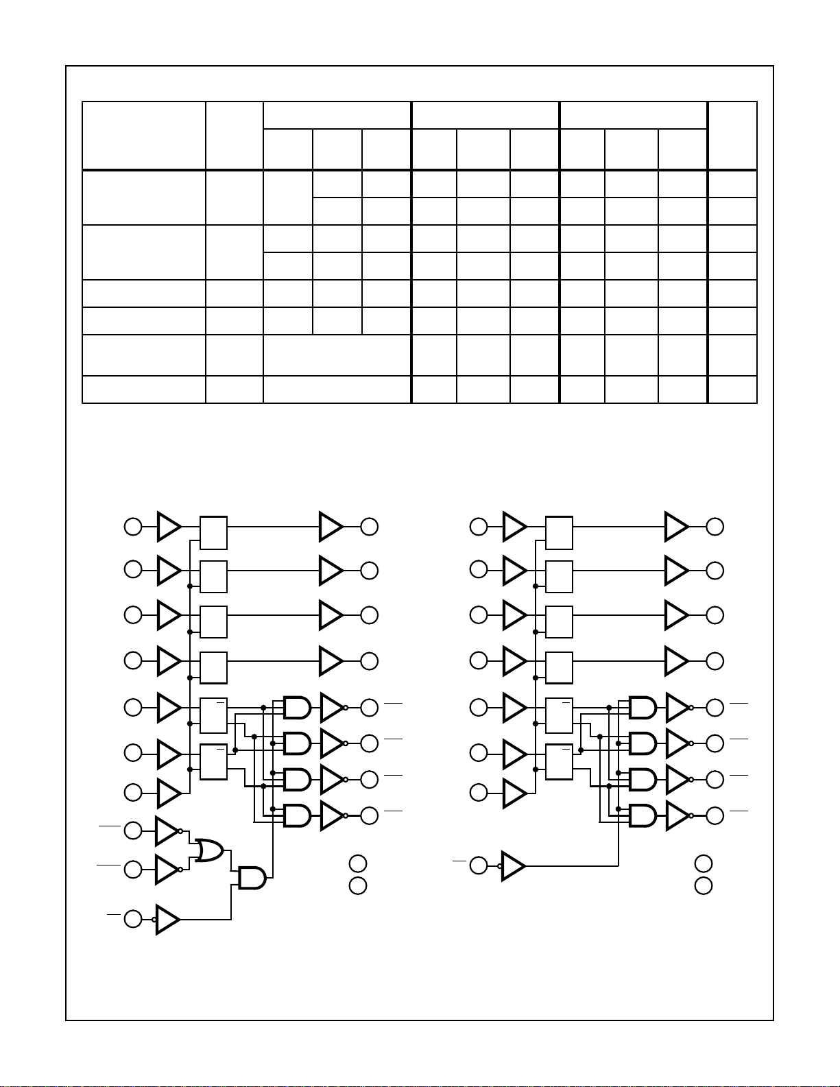
MA0
MA1
MA2
MA3
MA4
MA5
CLOCK
MRD
MWR
CE
7
6
5
4
3
2
1
8
9
11
DCQ
DCQ
DCQ
DCQ
DCQ
Q
DCQ
Q
V
V
DD
SS
19
A8
18
A9
17
A10
16
A11
15
CS0
14
CS1
13
CS2
12
CS3
20
=
10
=
CLOCK
MA0
MA1
MA2
MA3
MA4
MA5
CE
7
6
5
4
3
2
1
8
DCQ
DCQ
DCQ
DCQ
DCQ
DCQ
17
A8
A9
16
15
A10
14
A11
13
CS0
Q
12
CS1
Q
V
V
DD
11
CS2
10
CS3
18
=
9
=
SS
FIGURE 1. FUNCTIONAL DIAGRAM FOR THE CDP1881C FIGURE 2. FUNCTIONAL DIAGRAM FOR THE CDP1882,
CDP1882C
4-3
Page 4

CDP1881C, CDP1882, CDP1882C
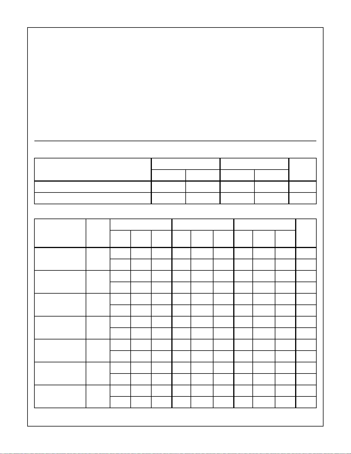
TRUTH TABLE
INPUTS OUTPUTS
(NOTE 1)
MWR
1 1 XXXX1111
X X 1XXX1111
0 X 01000111
0 X 01101011
0 X 01011101
0 X 01111110
0 X 0 0 X X Previous State
X 0 01000111
X 0 01101011
X 0 01011101
X 0 01111110
X 0 0 0 X X Previous State
NOTE:
1. CDP1881C Only
(NOTE 1)
MRD CE CLK MA4 MA5 CS0 CS1 CS2 CS3
INPUTS OUTPUTS
CE CLK MA0, MA1, MA2, MA3 A8, A9, A10, A11
X111
X100
X 0 X Previous State
Logic 1 = High, Logic 0 = Low, X = Don’t Care
Dynamic Electrical Specifications at T
= -40oC to +85oC, VDD± 5%, tR, tF = 20ns, VIH = 0.7 VDD, VIL = 0.3 VDD, CL = 100pF,
A
(See Figure 1)
CDP1882 CDP1881C, CDP1882C
PARAMETER
Minimum Setup Time t
MACL
V
DD
(V)
5 - 10 35 - 10 35 ns
(NOTE 1)
TYP
(NOTE 2)
MAX MIN
(NOTE 1)
TYP
(NOTE 2)
MAX
UNITSMIN
Memory Address to CLOCK 10 - 8 25 - - - ns
Minimum Hold Time t
CLMA
5-825-825ns
Memory Address After CLOCK 10 - 8 25 - - - ns
Minimum CLOCK Pulse Width t
CLCL
5 - 50 75 - 50 75 ns
10 - 25 40 - - - ns
4-4
Page 5

CDP1881C, CDP1882, CDP1882C
Dynamic Electrical Specifications at T
(See Figure 1) (Continued)
PARAMETER
PROPAGATION DELAY TIMES
Chip Enable to Chip Select t
MRD or MRW to Chip Select (Note 3) t
CLOCK to Chip Select t
CLOCK to Address t
Memory Address to Chip Select t
Memory Address to Address t
CECS
MCS
CLCS
CLA
MACS
MAA
= -40oC to +85oC, VDD± 5%, tR, tF = 20ns, VIH = 0.7 VDD, VIL = 0.3 VDD, CL = 100pF,
A
CDP1882 CDP1881C, CDP1882C
V
DD
(V)
(NOTE 1)
TYP
(NOTE 2)
MAX MIN
(NOTE 1)
TYP
(NOTE 2)
MAX
UNITSMIN
5 - 75 150 - 75 150 ns
10 - 45 100 - - - ns
5 - 75 150 - 75 150 ns
10 - 40 100 - - - ns
5 - 100 175 - 100 175 ns
10 - 65 125 - - - ns
5 - 100 175 - 100 175 ns
10 - 65 125 - - - ns
5 - 100 175 - 100 175 ns
10 - 75 125 - - - ns
5 - 80 125 - 80 125 ns
10 - 40 60 - - - ns
NOTES:
1. Typical values are for TA = 25oC.
2. Maximum limits of minimum characteristics are the values above which all devices function.
3. For CDP1881C type only.
CE
CS0, CS1, CS2, CS3
MRD OR MWR
CS0, CS1, CS2, CS3
MA0 - MA5
CLOCK
CS0, CS1, CS2, CS3
A8 - A11
t
CECS
(A) CHIP ENABLE TO CHIP SELECT PROPAGATION DELAY
t
MCS
(B)
MRD OR MWR TO CHIP SELECT PROPAGATION DELAY (CDP1881C ONLY)
t
MACL
t
CLA
t
CLCS
t
CLCL
VALID CHIP ENABLE
t
CLMA
t
MACS
t
t
MCS
MAA
t
MACS
t
t
MAA
CECS
(C) MEMORY ADDRESS SETUP AND HOLD TIME
FIGURE 3. TIMING WAVEFORMS
4-5
Page 6

CDP1881C, CDP1882, CDP1882C
Signal Descriptions/Pin Functions
CLOCK: Latch-Input Control - a high at the clock input will
allow data to pass through the latch to the output pin. Data is
latched on the high to low transition of the clock input. This
input is connected to TPA in CDP1800-series systems.
MA0 - MA3: Address inputs to the high-byte address
latches.
MA4 - MA5: High byte address inputs decoded to produce
chip selects
MRD, MWR: MEMOR Y READ (
(
MWR) signal inputs on the CDP1881C. A low at either
input, when the
select outputs (
CE: CHIP ENABLE input - a low at the
CDP1882, CDP1882C will enable the chip select decoder. A
low at the
either
A high on this pin forces
(false) state.
A8 - A11: Latched high-byte address outputs.
CS0 - CS3: One of four latched and decoded Chip Select
outputs.
V
, VSS: Power and ground pins, respectively.
DD
CS0 - CS3.
MRD) and MEMORY WRITE
CE pin is low, will enable the decoder chip
CS0 - CS3).
CE input of
CE input of CDP1881C, coincident with a low at
MRD or MRW pin, will enable the chip select decoder.
CS0, CS1, CS2, and CS3 to a high
Application Information
The CDP1881C, CDP1882, CDP1882C can interface
directly with the multiplexed address bus of the CDP1800series microprocessor family at maximum clock frequency. A
single CDP1881C or CDP1882 is capable of decoding up to
16K-bytes of memory.
The CDP1881C is provided with
controlling bus contention, and is especially useful for interfacing with RAMs that do not have an output enable function
(
OE). Figure 4 shows the CDP1881C in a minimum system
configuration which includes the CDP1833 ROM (1K x 8)
and two 2K x 8 RAMS. The CDP1881C in this example performs the following functions:
1) Latch and decode high-order address bits for use as chip
selects.
2) Gate chip selects with
contention with the CPU.
3) Latch high-order address bits A8 to A11.
A system using the CDP1882 is shown in Figure 5. The
CDP1882 performs the memory address latch and decoder
functions. Note that the RAM has an output enable (
which eliminates the need for
latch/decoder. Instead, the
the RAM output enable (
OE) pin.
In Figure 6 the CDP1882 is used to decode a 16K-byte ROM
system consisting of four CDM5332s.
MRD and MWR inputs for
MRD and MWR to prevent bus
OE) pin
MRD and MWR inputs on the
MRD line is connected directly to
WAIT
CLR
ADDRESS BUS
A0 - A7
TPA
CDP1800
SERIES
CPU
MRD
MWR
NOTE: CEA = CE RAM NUMBER 1
CEB = CE RAM NUMBER 2
FIGURE 4. MINIMUM 1800-SERIES USING THE CDP1881C
TPA
CDP1883
1K x 8
ROM
CEO
MRD
DATA BUS
MA0 - MA5
CLK
CDP1881C
LATCH/
DECODER
CE
MRD
MWR
A11
CS0
CS1
CS2
CS3
A8 - A10
A0 - A7
(2) 2K x 8
RAMS
CEA (NOTE 1)
CEB (NOTE 1)
CS
W
R/
4-6
Page 7

CDP1881C, CDP1882, CDP1882C
CDP1882
LATCH/
DECODER
CS3
CLK
CS2
CE
CS1
CS0
MA0 - MA5
A8 - A11
TO OTHER
CHIP SELECTS
CLR
CDP1800
SERIES
CPU
MRD
MWR
WAIT
TPA
ADDRESS BUS
A8 - A11
A0 - A7
CDM5332
CSI/OE
DATA BUS
ADDRESS BUS
CS2
4K x 8
ROM
FIGURE 5. CDP1800-SERIES SYSTEM USING THE CDP1882
CDP1882
LATCH/
DECODER
CS3
CLK
CE
MA0 - MA5
CS2
CS1
CS0
A8 - A11
A8 - A10
CE
A0 - A7
CDM6116A
2K x 8
RAM
OE
WE
CLR
TPA
CDP1800
SERIES
CPU
MRD
WAIT
ADDRESS BUS
ADDRESS BUS
A8 - A11
CS2
A0 - A7
CDM5332
4K x 8
ROM
CSI/OE
A8 - A11
A0 - A7
CDM5332
4K x 8
CSI/OE
DATA BUS
ROM
CS2
A8 - A11
CS2
A0 - A7
CDM5332
4K x 8
ROM
CSI/OE
FIGURE 6. 6K-BYTE ROM SYSTEMS USING THE CDP1882
4-7
A8 - A11
CS2
A0 - A7
CDM5332
4K x 8
ROM
CSI/OE
Page 8

CDP1881C, CDP1882, CDP1882C
All Intersil semiconductor products are manufactured, assembled and tested under ISO9000 quality systems certification.
Intersil products are sold by description only. Intersil Corporation reserves the right to make changes in circuit design and/or specifications at any time without
notice. Accordingly, the reader is cautioned to verify that data sheets are current before placing orders. Information furnished by Intersil is believed to be accurate
and reliable. However, no responsibility is assumed by Intersil or its subsidiaries for its use; nor for any infringements of patents or other rights of third parties which
may result from its use. No license is granted by implication or otherwise under an y patent or patent rights of Intersil or its subsidiaries.
For information regarding Intersil Corporation and its products, see web site http://www.intersil.com
Sales Office Headquarters
NORTH AMERICA
Intersil Corporation
P. O. Box 883, Mail Stop 53-204
Melbourne, FL 32902
TEL: (407) 724-7000
FAX: (407) 724-7240
EUROPE
Intersil SA
Mercure Center
100, Rue de la Fusee
1130 Brussels, Belgium
TEL: (32) 2.724.2111
FAX: (32) 2.724.22.05
ASIA
Intersil (Taiwan) Ltd.
Taiwan Limited
7F-6, No. 101 Fu Hsing North Road
Taipei, Taiwan
Republic of China
TEL: (886) 2 2716 9310
FAX: (886) 2 2715 3029
8
 Loading...