

Page 1
CDP1879,
CDP1879C-1
March 1997
Features
• CPU Interface for Use with General-Purpose
Microprocessors
• Time Of Day/Calendar
• Reads Seconds, Minutes, Hours
• Reads Day of Month and Month
• Alarm Circuit With Seconds, Minutes or Hours
Operation
• Power Down Mode
• Separate Clock Output Selects 1 of 15 Square Wave
Signals
• Interrupt Output Activated By Clock Output and/or
Alarm Circuit
• Date Integrity Sampling for Clock Rollover Eliminated
• On-Board Oscillator:
- Crystal Operation CDP1879 at 10V. . . . . . . 4.19MHz,
2.09MHz or 1.048MHz
- Crystal Operation CDP1879C-1 at 5V . . . . . 4.19MHz,
2.09MHz or 1.048MHz or 32kHz
- External Clock Operation at 10V or 5V. . . . 4.19MHz,
2.09MHz, 1.048MHz or 32kHz
• Addressable in Memory Space or CDP1800 Series I/O
Mode
• Low Standby (Timekeeping) Voltage with External Clock
• Related Literature
- AN7275, Guide to the Use of CD1879 and
CDP1879C1 Real Time Clock
Pinout
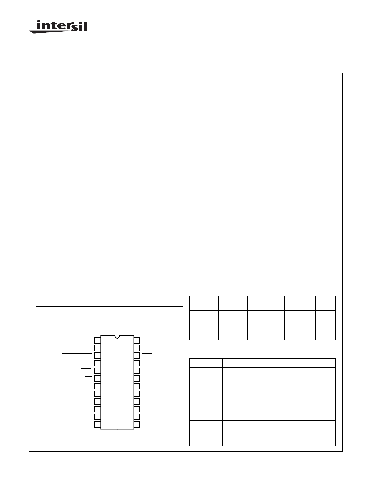
CDP1879, CDP1879C-1 (PDIP, SBDIP)
TOP VIEW
INT
RESET
POWER DOWN
RD
MEM
IO/
TPB/
WR
TPA
CS
A2
A1
A0
V
SS
1
2
3
4
5
6
7
8
9
10
11
12
24
V
DD
XTAL
23
22
XTAL
CLK
21
OUT
DB7
20
DB6
19
DB5
18
DB4
17
DB3
16
DB2
15
DB1
14
DB0
13
CMOS Real-Time Clock
Description
The CDP1879 real-time clock supplies time and calendar information
from seconds to months in BCD format. It consists of 5 separately
addressable and programmable counters that divide down an oscillator
input. The clock input can have any one of 4 possible frequencies,
allowing flexibility in the choice of crystal or external clock sources.
Using an external 32kHz clock source, timekeeping can be performed
down to 2.5V (see Standby (Timekeeping)Voltage Operation).
The device can be memory-mapped for use with any general-purpose
microprocessor and has the additional capability of operating in the
CDP1800 series input/output mode.
The real-time clock functions as a time-of-day/calendar with an alarm
capability that can be set for combinations of seconds, minutes or
hours. Alarm time is configured by loading alarm latches that activate
an interrupt output through a comparator when the counter and alarm
latch v alues are equal.
Fifteen selectable square-wave signals are available as a separate
clock output signal and can also activate the interrupt output. A status
register is available to indicate the interrupt source. The value in an 8 bit
control register determines the operational characteristics of the de vice,
by selecting the prescaler divisor and the clock output, and controls the
load and alarm functions.
A transparent “freeze” circuit preclude clock rollover during counter and
latch access times to assure stable and accurate values in the counters
and alarm latches.
The CDP1879 is functionally identical to the CDP1879C-1. The
CDP1879 has a recommended operating voltage range of 4V to 10.5V,
and the CDP1879C-1 has a recommended operating voltage range of
4V to 6.5V . The CDP1879 and the CDP1879C-1 are supplied in 24 lead
hermetic dual-in-line side-brazed ceramic packages (D suffix) and 24
lead dual-in-line plastic packages (E suffix
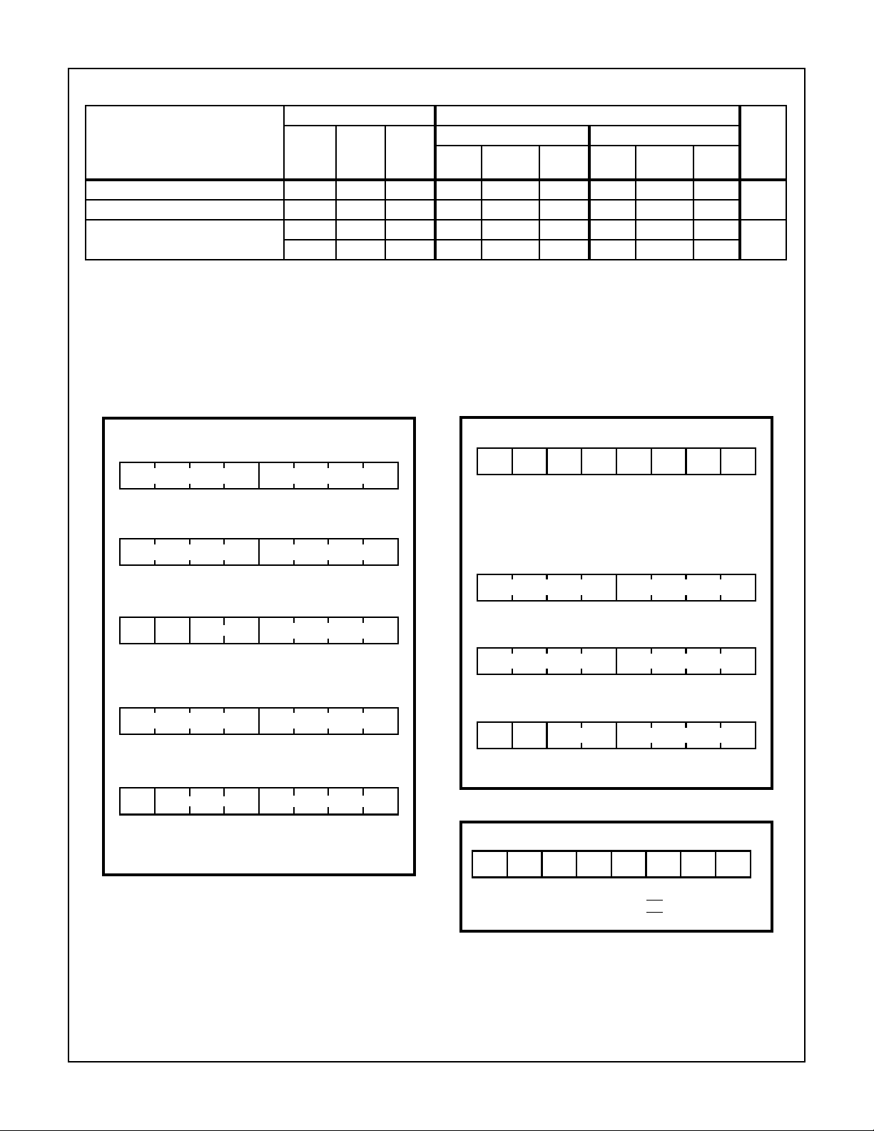
Ordering Information
TEMP
P A CKAGE
PDIP -40oC to
SBDIP -40oC to
Burn-In CDP1879CD1X - D24.6
RANGE 5V 10V
CDP1879CE1 CDP1879E E24.6
+85oC
CDP1879CD1 - D24.6
+85oC
CDP1879 Modes of Operation
OPERATION FUNCTION
Read 1. Seconds, minutes, hours, date and month counters
Write 1. Control register to set device operation
Power Down 1. Three-state interrupt output with active alarm or
Interrupt 1. Clock out as source
2. Status register to identify interrupt source
2. Seconds, minutes, hours, date and month counters
3. Alarm latches for alarm time
clock out circuitry for wake-up control
2. Data bus and address inputs are “DON’T CARE”
2. Alarm time as source
3. Either interrupt can occur during normal or power
down mode
).
PKG.
NO.
CAUTION: These devices are sensitive to electrostatic discharge; follow proper IC Handling Procedures.
http://www.intersil.com or 407-727-9207
| Copyright © Intersil Corporation 1999
4-104
File Number
1360.2
Page 2
CDP1879, CDP1879C-1
Absolute Maximum Ratings Thermal Information
DC Supply Voltage Range, V
(Voltage referenced to VSS Terminal)
CDP1879 . . . . . . . . . . . . . . . . . . . . . . . . . . . . . . . . -0.5V to +11V
CDP1879C-1. . . . . . . . . . . . . . . . . . . . . . . . . . . . . . . -0.5V to +7V
Input Voltage Range, All Inputs . . . . . . . . . . . . . . -0.5 to VDD +0.5V
DC Input Current, Any One Input . . . . . . . . . . . . . . . . . . . . . . ±10mA
Device Dissipation Per Output Transistor. . . . . . . . . . . . . . . . 40mW
For TA = Full Package Temperature Range
(All Package Types)
CAUTION: Stresses above those listed in “Absolute Maximum Ratings” may cause permanent damage to the device. This is a stress only rating and operation
of the device at these or any other conditions above those indicated in the operational sections of this specification is not implied.
DD
Thermal Resistance (Typical) θJA (oC/W) θJC (oC/W)
PDIP Package. . . . . . . . . . . . . . . . . . . 60 N/A
SBDIP Package. . . . . . . . . . . . . . . . . . 50 12
Operating Temperature Range (TA)
Package Type D, H . . . . . . . . . . . . . . . . . . . . . . .-55oC to +125oC
Package Type E. . . . . . . . . . . . . . . . . . . . . . . . . . .-40oC to +85oC
Storage Temperature Range (T
Lead Temperature (During Soldering). . . . . . . . . . . . . . . . . .+265oC
At Distance 1/16 ±1/32 in. (1.59± 0.79mm) From Case for 10s Max
). . . . . . . . . . . .-65oC to +150oC
STG
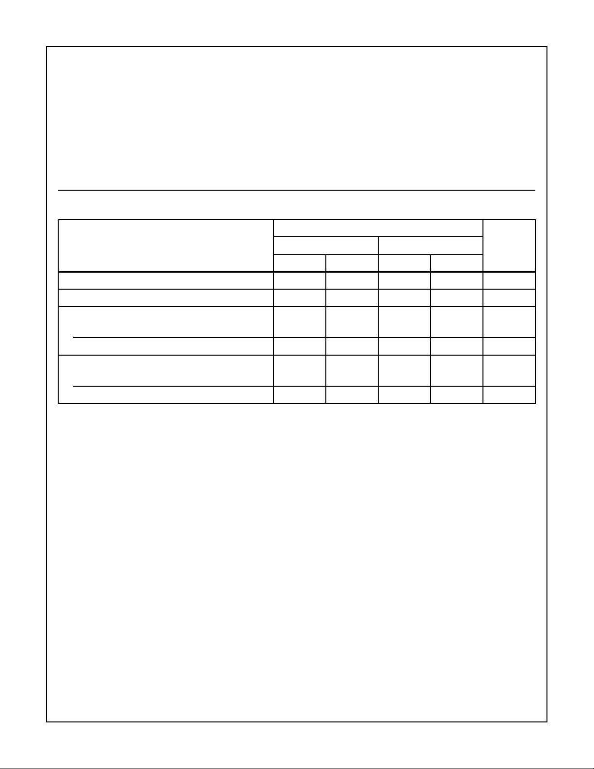
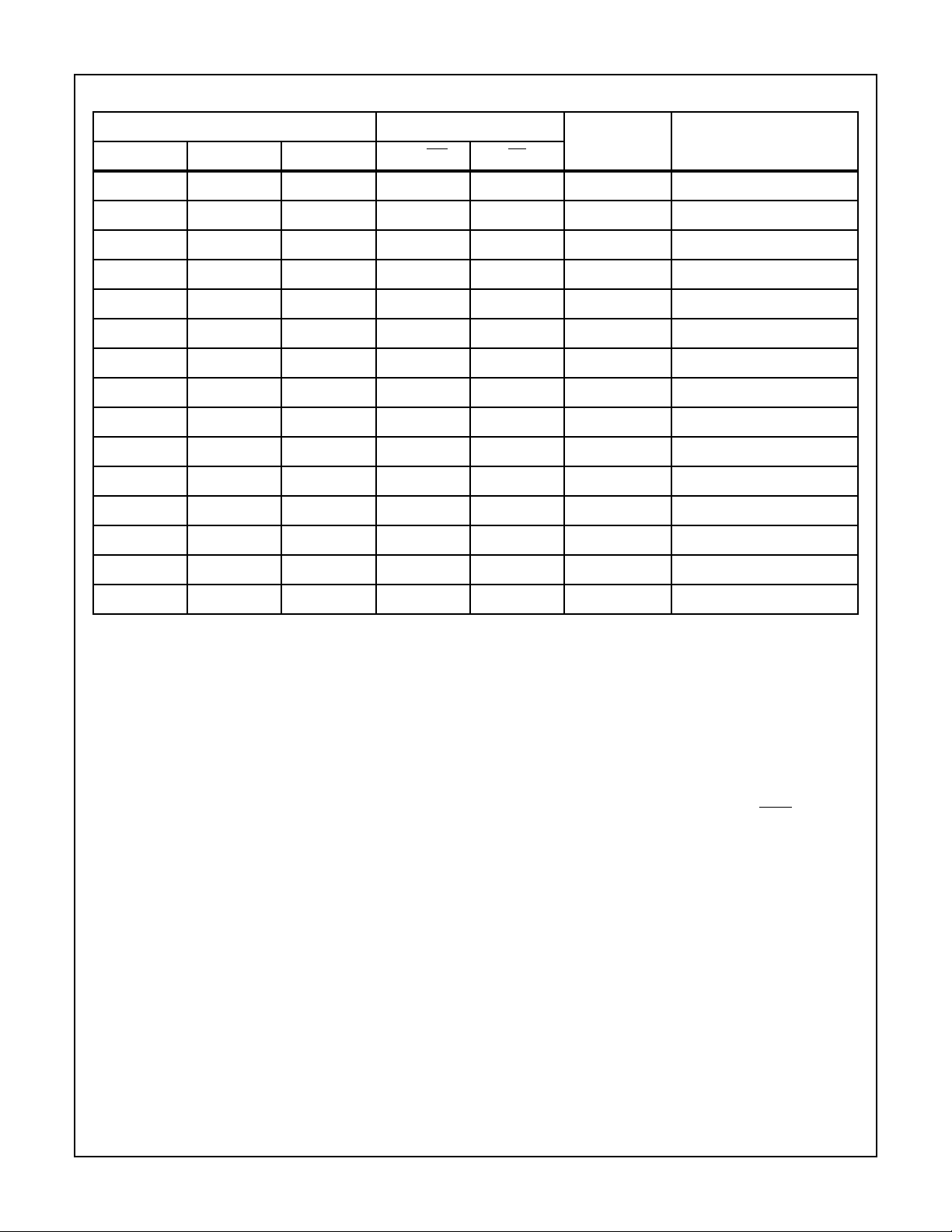
Operating Conditions at T
PARAMETER
DC Operating Voltage Range 4 10.5 4 6.5 V
Input Voltage Range V
DC Standby (Timekeeping) Voltage (Note 1), V
TA = -40oC to +85oC (Note 2) 3 - 3 - V
TA = 0o to +70oC 2.5 - 2.5 V
Clock Input Rise or Fall Time, tR, t
VDD = 5V - 10 - 10 µs
VDD = 10V - 1 - - µs
NOTES:
1. Timekeeping function only, no READ/WRITE accesses, 32kHz external frequency source only, no crystal operation.
2. See Standby (Timekeeping) Voltage Operation.
= FuIl Package-Temperature Range, Unless Otherwise specified. For maximum reliability, operating con-
A
ditions should be selected so that operation Is always within the following ranges:
LIMITS
CDP1879 CDPl879C-1
MIN MAX MIN MAX
SS
STBY
F
V
DD
V
SS
V
DD
UNITS
V
4-105
Page 3
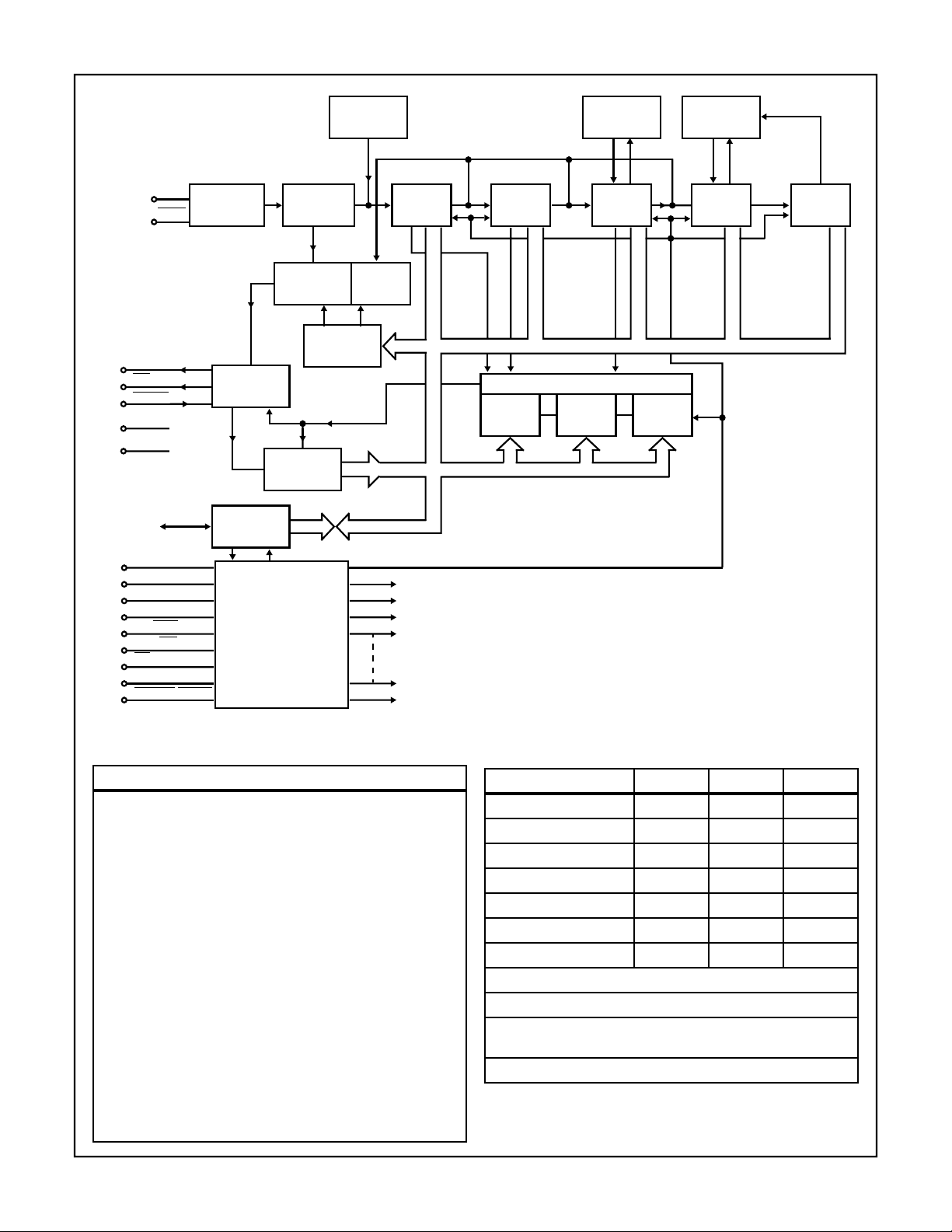
CDP1879, CDP1879C-1
XTAL
OSCILLATOR SECOND
XTAL
CLOCK OUT
INT
RESET
V
DD
V
SS
DB0-DB7
A0
A1
A2
TPA
MEM
I-O
TPB/WR
RD
CS
POWER DOWN
PRESCALE
PRESCALE
SELECT
CLOCK AND
INT. LOGIC
INT. STATUS
REGISTER
I/O
INTERFACE
ADDRESS DECODE
AND
CONTROL LOGIC
FREEZE
CIRCUIT
CONTROL
REGISTER
CLOCK
SELECT
AM - PM
AND
HOUR LOGIC
MINUTE HOUR DAY MONTH
8-BIT DATA BUS
COMPARATOR
SECOND
LATCH
MINUTE
LATCH
HOUR
LATCH
CALENDAR
LOGIC
FIGURE 1. REAL-TIME CLOCK FUNCTIONAL DIAGRAM
TABLE 1.
CONTROL REGISTER BIT ASSIGNMENT
Bit 1, 0
Frequency 00
Select 01
10
11
32768Hz
1.048576MHz
2.097152MHz
4.194304MHz
Bit 2
Start/Stop 1 = Start
0 = Stop
Bit 3
Counter/Latch Control
“0” = Write to Counter and disable alarm
“1” = Write to and enable alarm Clock Select
Bit 7, 6, 5, 4
0000 - disableµs
0001 - 488.2µs
0010 - 976.5µs
0011 - 1953.1µs
0100 - 3906.2µs
0101 - 7812.5µs
0110 - 15.625ms
0111 - 31.25ms
1000 - 62.5ms
1001 - 125ms
1010 - 250ms
1011 - 500ms
1100 - sec.
1101 - min.
1110 - hour
1111 - day
TABLE 2.
ADDRESSES A2 A1 A0
Latch, Counter Seconds 0 1 0
Latch, Counter Minutes 0 1 1
Latch, Counter Hours 1 0 0
Counter, Day 1 0 1
Counter, Month 1 1 0
Control, Register 1 1 1
Status Register 1 1 1
MSB of Hours Counters (Bit 7) is an AM-PM Bit. 0 = AM; 1 = PM
Bit 6 of Hours Counter Controls 12/24 hr. 1 = 12 Hr: 0 = 24 Hr.
Status Register: Bit 7 MSB = Alarm
Interrupt Source: Bit 6 = Clock.
MSB of Month Counter (Bit 7) is a Leap Year Bit 0 = No, 1 = Yes.
4-106
Page 4
CDP1879, CDP1879C-1
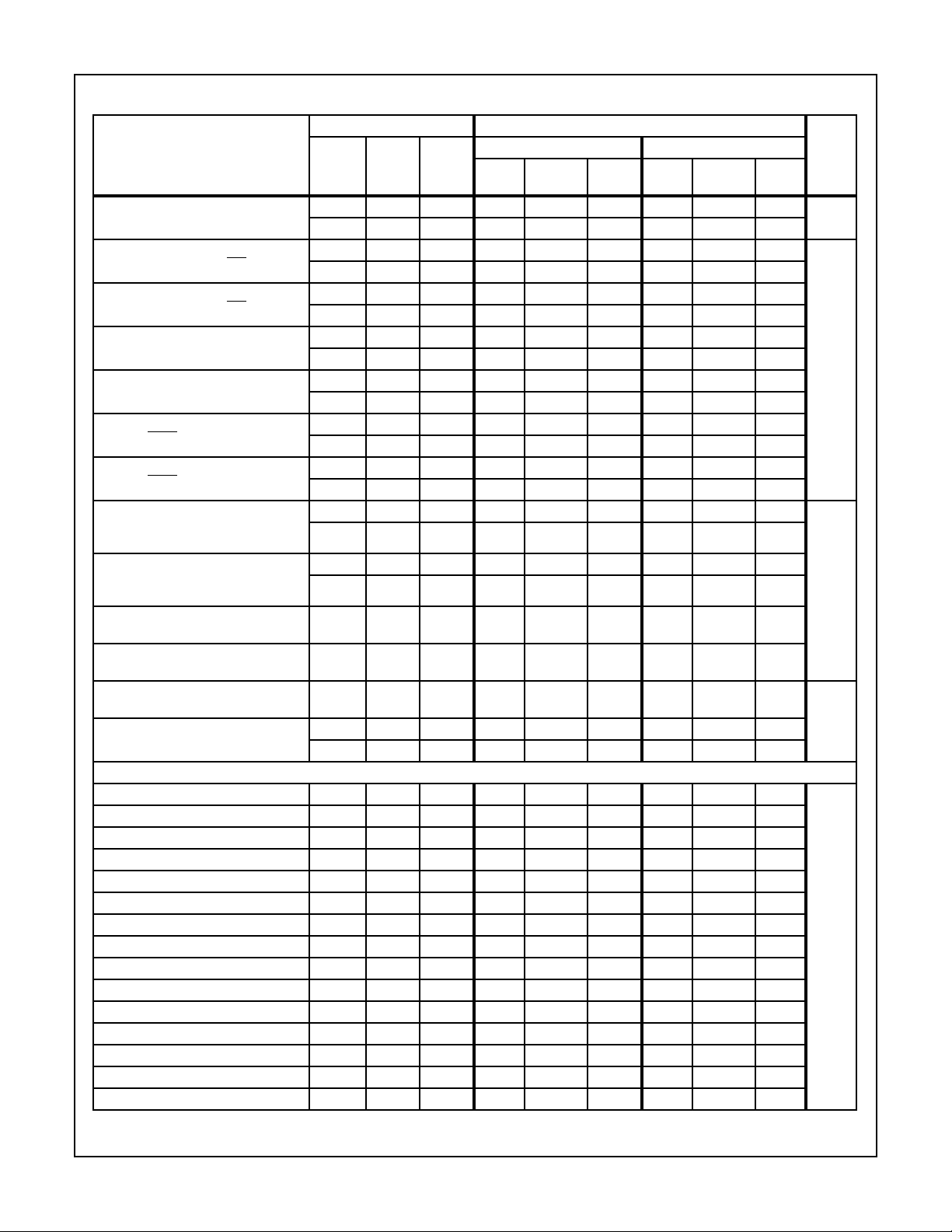
Static Electrical Specifications at T
-40oC to +85oC VDD± 5%, Unless Otherwise Specified
A
CONDITIONS LIMITS
CDP1879 CDPl879C-1
PARAMETER
Ouiescent Device Current I
V
(V)
DD
V
O
(V)
V
IN
DD
(V)
MIN
(NOTE 1)
TYP MAX MIN
(NOTE 1)
TYP MAX
0, 5 5 - 0.01 50 - 0.02 200 µA
0, 10 10 - 1 200 - - -
Output Low Drive (Sink)
Current, Data Bus and INT l
Output High Drive (Source)
Current, Data Bus and INT I
Output Low Drive (Sink)
Current, Clock Out l
Output High Drive (Source)
Current, Clock Out I
Output Low Drive (Sink)
Current, XTAL Out l
Output High Drive (Source)
Current, XTAL Out I
Output Voltage
Low-Level V
(Note 2)
Output Voltage
High Level V
(Note 2)
Input Low Voltage V
Input High Voltage V
Input Leakage Current I
Three-State Output
Leakage Current I
OL
OH
OL
OH
OL
OH
OL
OH
IL
IH
IN
OUT
0.4 0, 5 5 1.8 4 - - - -
0.5 0,10 10 3.6 7 - - - -
4.6 0, 5 5 -1.1 -2.3 - -1.1 -2.3 -
9.5 0,10 10 -2.6 -4.4 - - - -
0.4 0, 5 5 0.6 1.4 - 0.6 1.4 -
0.5 0,10 10 1.2 3 - - - -
4.6 0, 5 5 -1.1 -2.3 - -1.1 -2.3 -
9.5 0,10 10 -2.6 -4.4 - - - -
0.4 0, 5 5 0.2 0.9 - 0.2 0.9 -
0.5 0,10 10 0.4 2 - - - -
4.6 0, 5 5 -0.15 -0.4 - -0.15 -0.4 -
9.5 0,10 10 -0.3 -0.7 - - - -
- 0, 5 5 - 0 0.1 - 0 0.1
- 0,10 10 - 0 0.1 - - -
- 0, 5 5 4.9 5 - 4.9 5 -
- 0, 10 10 9.9 10 - - - -
0.5, 4.5
0.5, 9.5
0.5, 4.5
0.5, 9.5
Any
Input
-
-
-
-
0, 5
0, 10
10
10
10
5
5
5
3.5
-
-
7
-
-
-
-
-
-
-
-
1.5
±1
±2
-
3
-
-
-
3.5
-
-
-
-
-
-
-
-
-
0, 5 0,5 5 - - ±1- - ±1
0,10 0,10 10 - - ±1--Operating Current (Note 3)
External Clock 32kHz - - 5 - 0.01 0.15 - 0.01 0.15
External Clock 1MHz - - 5 - 0.2 1 - 0.2 1
External Clock 2MHz - - 5 - 0.35 1.5 - 0.35 1.5
External Clock 4MHz - - 5 - 0.7 2 - 0.7 2
External Clock 32kHz - - 10 - 0.03 0.25 - - External Clock 1MHz - - 10 - 0.4 2 - - External Clock 2MHz - - 10 - 0.8 3 - - External Clock 4MHz - - 10 - 1.6 4.5 - XTAL Oscillator (Note 4) 32kHz - - 5 - 0.1 0.25 - 0.1 0.25
XTAL Oscillator (Note 4) 1MHz - - 5 - 0.3 0.5 - 0.3 0.5
XTAL Oscillator (Note 4) 2MHz - - 5 - 0.4 0.6 - 0.4 0.6
XTAL Oscillator (Note 4) 4MHz - - 5 - 0.6 0.8 - 0.6 0.8
XTAL Oscillator (Note 4) 1MHz - - 10 - 1.6 3 - - XTAL Oscillator (Note 4) 2MHz - - 10 - 1.8 3.5 - - XTAL Oscillator (Note 4) 4MHz - - 10 - 2 5 - - -
UNITS
mA
V
1.5
-
-
-
±1
µA
mA
4-107
Page 5
CDP1879, CDP1879C-1
Static Electrical Specifications at T
-40oC to +85oC VDD± 5%, Unless Otherwise Specified (Continued)
A
CONDITIONS LIMITS
PARAMETER
Input Capacitance C
Output Capacitance C
IN
OUT
Maximum Clock Rise tR, t
and Fall Times
V
(V)
- - - - 5 7.5 - 5 7.5 pF
- - - - 10 15 - 10 15
F
--5--10--10µs
--10--1---
V
O
(V)
V
IN
DD
(V)
NOTES:
1. Typical values are for TA = 25oC and nominal VDD.
2. IOL = IOH = 1µA.
3. Operating current measured with clockout = 488.2µs and no load.
4. See Table 3 and Figure 6 for oscillator circuit information.
Programming Model
WRITE AND READ REGISTERS WRITE ONLY REGISTERS
BCD FORMAT
DB7 DB0
TENS 0-5 UNITS 0-9
SECONDS COUNTER (00-59)
DB7 DB0
TENS 0-5
MINUTES COUNTER (00-59)
DB7 DB0
DB6
X X TENS 0-2
HOURS COUNTER (01 - 12 OR 00-23)
DB7 0=AM, 1=PM
DB6 0=24 HR, 1=12 HR
DB7 DB0
TENS 0-3 UNITS 0-9
DAY OF MONTH COUNTER
(01-28, 29, 30, 31)
DB7 DB0
X TENS 0 OR 1
MONTH COUNTER
(JAN=1 DEC=12)
DB7 0=NO LEAP YEAR
1=LEAP YEAR
UNITS 0-9
UNITS 0-9
UNITS 0-9
CDP1879 CDPl879C-1
(NOTE 1)
MIN
TYP MAX MIN
DB7 DB0
7
6543210
CONTROL REGISTER
DB0-DB1 - FREQUENCY SELECT
DB2 - START/STOP
DB3 - COUNTER/ALARM LATCH CONTROL
DB4-DB7 - CLOCK OUTPUT SELECT
DB7 DB0
TENS 0-5 UNITS 0-9
SECONDS ALARM LATCH (00-59)
DB7 DB0
TENS 0-5 UNITS 0-9
MINUTES ALARM LATCH (00-59)
DB6
DB7 DB0
TENS 0-2 UNITS 0-9XX
HOURS ALARM LATCH (01-12 OR 00-23
12 HR, DB7=0 AM, 1=PM
24 HR, DB7=X
(NOTE 1)
TYP MAX
READ ONLY REGISTER
DB7 DB0
DB6
X
X000000
UNITS
4-108
INTERRUPT STATUS REGISTER
DB7=1 ALARM CIRCUIT ACTIVATED INT.
DB6=1 CLOCK OUTPUT ACTIVATED
INT.
Page 6
CDP1879, CDP1879C-1
REGISTER TRUTH TABLE
ADDRESS ACTIVE SIGNAL
0 1 0 X - 0 Write Seconds Counter
0 1 0 - X 0 Read Seconds Counter
0 1 1 X - 0 Write Minutes Counter
0 1 1 - X 0 Read Minutes Counter
1 0 0 X - 0 Write Hours Counter
1 0 0 - X 0 Read Hours Counter
1 0 1 X - 0 Write Date Counter
1 0 1 - X 0 Read Date Counter
1 1 0 X - 0 Write Month Counter
1 1 0 - X 0 Read Month Counter
0 1 0 X - 1 Write Seconds Alarm Latch
0 1 1 X - 1 Write Minutes Alarm Latch
1 0 0 X - 1 Write Hours Alarm Latch
1 1 1 X - - Write Control Register
BIT 3 CONTROL
REGISTER REGISTER OPERATIONA2 A1 AO TPB/WR RD
1 1 1 - X - Read Int. Status Register
General Operation
The real-time clock contains seconds, minutes, and hours,
date and month counters that hold time of day/calendar
information (see Figure 2). The frequency of an intrinsic
oscillator is divided down to supply a once-a-second signal
to the counter series string. The counters are separately
addressable and can be written to or read from.
The real-time clock contains seconds, minutes and hour
write-only alarm latches that store the alarm time (see Figure 3). When the value of the alarm latches and counters are
equal, the interrupt output is activated. The interrupt output
can also be activated by a clock output transition. The clock
output is derived from the prescaler and counters and can
be one of 15 square-wave signals. The value in the readonly interrupt status register identifies the interrupt source.
Operational control of the real-time clock is determined by
the byte in a write-only control register. The 8-bit v alue in this
register determines the correct divisor for the prescaler, a
data direction and alarm enable bit, clock output select, and
start/stop control (see Figure 4).
Data transfer and addressing are accomplished in two
modes of operation, memory mapping and I/O mapping
using the CDP1800-series microprocessors. The mode is
selected by the level on an input pin. (IO/
mapping implies use of the address lines as chip selects and
address inputs during linear selection or partial or full decoding methods. I/O mapping with the CDP1800-series microprocessors involves use of the N line outputs in conjunction
with input and output instructions to transfer data to and from
memory.
MEM). Memory
4-109
Page 7

CDP1879, CDP1879C-1
XTAL
OSCILLATOR SECOND
XTAL
CLOCK OUT
INT
RESET
V
DD
V
SS
DB0-DB7
A0
A1
A2
TPA
IO/
MEM
TPB/
WR
RD
CS
POWER DOWN
PRESCALE
PRESCALE
SELECT
CLOCK AND
INT. LOGIC
INT. STATUS
REGISTER
I/O
INTERFACE
ADDRESS DECODE
AND
CONTROL LOGIC
FREEZE
CIRCUIT
CONTROL
REGISTER
CLOCK
SELECT
AM - PM
AND
HOUR LOGIC
MINUTE HOUR DAY MONTH
8-BIT DATA BUS
COMPARATOR
SECOND
LATCH
MINUTE
LATCH
HOUR
LATCH
CALENDAR
LOGIC
FIGURE 2. FUNCTIONAL DIAGRAM - TIME COUNTERS HIGHLIGHTED
4-110
Page 8

CDP1879, CDP1879C-1
XTAL
OSCILLATOR SECOND
XTAL
CLOCK OUT
INT
RESET
V
DD
V
SS
DB0-DB7
A0
A1
A2
TPA
MEM
IO/
TPB/
WR
RD
CS
POWER DOWN
PRESCALE
PRESCALE
SELECT
CLOCK AND
INT. LOGIC
INT. STATUS
REGISTER
I/O
INTERFACE
ADDRESS DECODE
AND
CONTROL LOGIC
FREEZE
CIRCUIT
CONTROL
REGISTER
CLOCK
SELECT
AM - PM
AND
HOUR LOGIC
MINUTE HOUR DA Y MONTH
8-BIT DATA BUS
COMPARATOR
SECOND
LATCH
MINUTE
LATCH
LATCH
HOUR
CALENDAR
LOGIC
FIGURE 3. FUNCTIONAL DIAGRAM - ALARM CIRCUIT, CLOCK OUTPUT, INTERRUPT, AND STATUS REGISTERS HIGHLIGHTED
Operational Sequence
Power is applied and the real-time clock is reset. This sets
the interrupt output pin high. After the CS pin is set high and
with address 7 on the address input lines, the control register
is loaded via the data bus to configure the clock.
With selective addressing, the seconds through month
counters are then written to and loaded to set the current time.
The real-time clock will now hold the current “wall clock” time,
with an accuracy determined by the crystal or external clock
used. If the alarm function is desired, the control register is
accessed and loaded again. This new byte will allow subsequent time data to be entered into the seconds, minutes and
hours alarm latches. This sequence is also used when selecting one of the 15 available cloc k-out signals.
If the alarm function was selected, the interrupt output pin
will be set low when the values in the seconds, minutes and
hour alarm latches match those in the seconds, minutes and
hour counters.
If one of the 15 sub second-to-day clock outputs is selected
by the byte in the control register, the clock output pin toggles at that frequency (50% duty cycle) The interrupt output
will also be set low on the first clock out negative transition.
The interrupt source (alarm or clock out) can be determined
by reading the interrupt status register. The clock output can
be deselected by placing zero in the upper nibble of the control register if the alarm function is selected as the only interrupt source.
Counters
The counter section consists of an on-board oscillator, a
prescaler and 5 counters that hold the time of day/calendar
information (see Figure 2).
1 of 4 possible external crystals determine the frequency of the
on-board oscillator (32,768Hz, 1.048576MHz, 2.097152MHz,
4.194304MHz). The oscillator output is divided down by a pres-
4-111
Page 9

CDP1879, CDP1879C-1
caler that supplies a once-a-second pulse to the counters. The
seconds counter divide the pulse by 60 and its output clocks
the minute counter every 60 seconds Further division by the
minutes, hours, day of month and month counters result in 5
counters holding data that reflect the time/calendar from seconds to months. The counters are addressed separately and
BCD data is transferred to and from via the data bus. The most
significant bit of the hours counter (Bit 7) is user programmed to
FREEZE
CIRCUIT
XTAL
XTAL
CLOCK OUT
INT
RESET
V
DD
V
SS
OSCILLATOR SECOND
CLOCK AND
INT. LOGIC
PRESCALE
PRESCALE
SELECT
CONTROL
REGISTER
INT. STATUS
REGISTER
CLOCK
SELECT
indicate AM or PM and will be inverted every 12th hour . (0=AM,
1=PM). Bit 6 of the hours counter is user programmed to
enable the hours counter for 12 or 24 hour operation.
(0=24,1=12). If 24-hour operation is selected, the AM-PM bit is
“don't care”, but still toggles ev ery 12th hour . Writing to the seconds counter resets the last 7 stages of the prescaler, allowing
time accuracy to approximately 1/100 of a second.
AM - PM
AND
HOUR LOGIC
MINUTE HOUR DAY MONTH
8-BIT DATA BUS
COMPARATOR
SECOND
LATCH
MINUTE
LATCH
HOUR
LATCH
CALENDAR
LOGIC
I/O
DB0-DB7
A0
A1
A2
TPA
MEM
IO/
TPB/WR
RD
CS
POWER DOWN
INTERFACE
ADDRESS DECODE
AND
CONTROL LOGIC
FIGURE 4. FUNCTIONAL DIAGRAM - CONTROL REGISTER HIGHLIGHTED
The most significant bit of the month counter is a Leap Year
bit. If it is set to “1”, the counter will count to February 29,
then roll to March 1. If set to “0” it will go to March 1st after
February 28th.
Alarm And Interrupt Status Register
The alarm circuit consists of 1) seconds, minutes and hour
alarm latches that hold the alarm time, 2) the outputs of the
seconds, minutes and hour counters, and 3) a comparator
that drives an interrupt output. The comparator senses the
counter and alarm latch values and activates the interrupt
output (active low) when they are equal (see Figure 3).
The write-only alarm latches have the same addresses as
their comparable counters. Bit 3 in the control register determines data direction to the latches or counters and alarm
enabling. For example, during a write cycle, if bit-3 in the
control register is a “1”, addressing the seconds counter or
alarm latch will load the seconds alarm latch from the data
bus and will enable the alarm function. Conversely, if bit-3 in
the control register is a “0”, addressing the seconds counter
or alarm latch during a write cycle will place the value on the
data bus into the seconds counter and will disable the alarm
function. The interrupt output can be activated by the alarm
circuit or the clock output. When an interrupt occurs, the
4-112
Page 10

CDP1879, CDP1879C-1
upper two bits of the interrupt status register identify the
interrupt source. The interrupt status register has the same
address as the control register. Addressing the interrupt status register with the
RD line active will place these register
bits on the data bus. Bits 0-5 are held low. A “1” in bit-6 represents a clock output transition as the interrupt source. A
“1” in bit-7 will identify the alarm circuit as the interrupt
source.
Activating the reset pin (active low) resets the hour latch to
“30” which prevents a match between alarm and time registers during an initialization procedure. Activating the reset
pin or writing to the control register resets the interrupt output (high) and clears the interrupt status register
Clock Output
One of 15 counter and prescaler overflows can be selected
as a 50% duty cycle output signal that is available at the
“clock out” pin. The frequency is selected by the upper nibble
in the control register. For example, selecting a one-second
clock output will result in a repetitive signal that will be high
for 500ms and low f or the same period. The high-to-low tr ansition of the output signal will set the clock bit in the status
register and activate the interrupt output. The level of the
“clock out” signal is derived from the value in the counter.
Example - if hours clock is selected and the minutes counter
holds 4 minutes, the clock out will be low for 26 minutes and
high for 30 minutes Thereafter, the clock out will toggle at a
50% duty cycle rate (see Table 1 and Figure 3).
CONTROL REGISTER (SEE TABLE 1 AND FIGURE 4)
BIT
7
6543210
CONTROL REGISTER BYTE
The 8-bit value in the control register determines the following:
1. Bit 0 and 1 - Frequency Select - Since there are one of 4
possible crystals the oscillator in the real-time clock can
operate with, these bit levels determine the prescaler divisor so that an accurate one second pulse is supplied to
the counter series string.
BIT 1 BIT 0 FREQUENCY
0 0 32,768Hz
0 1 1.048576MHz
1 0 2.097152MHz
1 1 4.194304MHz
2. Bit 2 - Start-Stop Control - Counter enabling is controlled
by the value at this location. A “1” will allow the counters
to function and a “0” in this location will disable the
counters.
3 Bit 3 - Counter/Latch Control - The level at this location
controls two functions. It is required since the counters
and alarm latches have the same addresses.
BIT
1) A “0” in bit-3 will direct subsequent data to or from
the counter selected and the alarm function will be
disabled.
2) A “1” in bit-3 will direct subsequent data to or from
the alarm latch and will enable the alarm.
4. Bits 4 to 7 - Clock Select - These bits select one of 15
square-wave signals that will be present at the “clockout” pin. If bit-4 to bit-7 are zero's, the clock output pin will
be high. If a clock is selected, the first high-to-low clock
out transition will activate the interrupt pin (active low) and
place a “1” in bit-6 of the status register. Writing to the
control register or activating the reset pin will set the interrupt pin high and reset the interrupt status register.
Normal operation requires the control register to be written
to and loaded first with a control word. However, subsequent
writing to a counter if a “clock out” is selected may cause an
interrupt out signal. Therefore, “clock-out” should be deselected by writing zero's into bit-4 through bit-7 if the interrupt
is used. When the counters are loaded, the control register
is again written to with the value in the upper nibble selecting
the “clock out” signal. See Table 1.
Read And Write Signals
When the IO/MEM pin is low, the real-time clock is enabled
for memory mapped operation. Data on the bus is placed in,
or read from a counter, alarm latch or register by 1) placing
the CS pin high, 2) selective addressing, 3) placing the
TPB/
WR pin low during a write cycle with the RD pin high or
4) setting the
TPB/
WR pin high.
RD pin low during a read cycle with this
The I/O mapping mode used with the CDP1800 series
microprocessor is selected by setting the IO/
The TPB/
WR pin on the real-time clock is connected to the
MEM pin high.
TPB output pin of the microprocessor. Data on that bus is
written to or read from the counters, latches and registers by
1) placing the CS pin high, 2) selective addressing utilizing
the microprocessor N lines and I/O instructions, 3) placing
the TPB/
WR pin high with the RD pin low during an output or
write operation (data is latched on TPB's trailing edge), 4)
setting the
RD line high during an input or read operation.
Data is placed on the bus by the real-time clock between the
trailing edges of TPA and TPB.
Freeze Circuit
Since writing to or reading from the counters or alarm
latches is performed asynchronously, the once-a-second
signal from the prescaler may pulse the counter series string
during these operations. This can result in erroneous data.
To avoid this occurring, a transparent “freeze” circuit' is incorporated into the real-time clock. This circuit is designed to
trap and hold the one-second input clock transition if it
occurs during access times. When the operations are completed, it is inserted into the counter series string. To utilize
the “freeze” circuit, address “1” (A0 = 1, A1 = 0, A2 = 0) is
selected first while performing a write operation. Read or
write accesses may now be performed with assurance the
data is stable. All operations must be concluded within
4-113
Page 11

CDP1879, CDP1879C-1
250ms of the address “1” access. In memory mapping any
dummy write operation after selecting address “1” will set the
“freeze” circuit. If using the I/O mode, a 61 output instruction
will perform the same function. There is no time restriction
on subsequent accesses as long as the read or write operations are preceded by selecting address “1”.
Power Down
Power down operation is initiated with a low signal on the
"POWER DOWN” input pin. In conjunction with the interrupt
output, it is used to supply external control circuits with a 3
level control signal. The operating current is not appreciably
reduced during “POWER DOWN” operation. When power
down is initiated, any inputs on the address or data bus are
ignored. The clock output is set low. The interrupt output is
three-stated. If enabled previously, the alarm circuitry is
active and will set the interrupt output pin low when alarm
time occurs. The interrupt output will also go low if a clock
was selected and an internal high-to-low transition occurs
during power down. The clock output pin will remain low. If
power down is initiated in the middle of a read or write
sequence, it will not become activated until the read or write
cycle is completed.
Pin Functions
VDD, VSS - Power and ground for device.
DB0 - DB7 - DATA BUS - 8-bit bidirectional bus that trans-
fers BCD data to and from the counters, latches and registers.
A0, A1, A2 - Address inputs that select a counter, latch or
register to read from or write to.
TPA - Strobe input used to latch the value on the chip select
pin. CS is latched on the trailing edge of TPA. During memory mapping, it is used to latch the high order address bit
used for the chip select. When the real-time clock is used
with other microprocessors, or when the high order address
of the CDP1800 series microprocessor is externally latched,
it is connected to V
gate the N lines.
IO/MEM - Tied low during memory mapping and high when
the input/output mode of the CDP1800 series microprocessor is used.
. In the input/output mode, it is used to
DD
Microprocessor Real-Time Clock
MRD . . . . . . . . . . . . . . . . . . . . . . . . . . . . . . . . . RD
TPB . . . . . . . . . . . . . . . . . . . . . . . . . . . . . . . . . . TPB/WR
TPA . . . . . . . . . . . . . . . . . . . . . . . . . . . . . . . . . . TPA
N LINES. . . . . . . . . . . . . . . . . . . . . . . . . . . . . . . ADDRESS LINES
IO/MEM . . . . . . . . . . . . . . . . . . . . . . . . . . . . . . . V
CS - CHIP SELECT - Used to enable or disable the inputs
and outputs. TPA is used to strobe and latch a positive level
on this pin to enable the device.
XTAL AND XTAL - The frequency of the internal oscillator is
determined by the value of the crystal connected to these
pins. “XTAL” may be driven directly by an external frequency
source.
Clock Out - 1 of 15 square wave frequencies will appear at
this pin when selected. During power down, this pin will be
placed low, and will be high during normal operation when
the clock is deselected.
Power Down - Power Down Control - A low on this pin will
place the device in the power down mode.
INT - Interrupt Output - A low on this pin indicates an active
alarm time or high-to-low transition of the “clock out” signal.
RESET - A low on this pin clears the status register and
places the interrupt output pin high.
DD
Frequency Input Requirements
The Real-Time Clock operates with the following frequency
input sources:
1. An external crystal that is used with the on-board oscilla-
tor. The oscillator is biased by a large feedback resistor
and oscillates at the crystal frequency (see Figure 6,
Table 3).
2. An external frequency input that is supplied at the XTAL
input.
XTAL is left open (see Figure 5). A typical external
oscillator circuit is shown in Figure 7 in section, “Standby
(Timekeeping) Voltage Operation”.
RD, TPB/WR - Direction Signals - Active signals that determine data direction flow. In the memory mapped mode, data
is placed on the bus from the counters or status register
when
RD pin is active.
Data is transferred to a counter, latch or the control register
when
RD is high and TPB/WR is active and latched on the
trailing edge (low to high) of the TPB/
In the input/output mode, data is placed on the bus from a
counter or status register when RD is not active between the
trailing edges of TPA and TPB. Data on the bus is written to a
counter, latch, or the control register during TPB when
active and latched on TPB's trailing edge. The following connections are required between the microprocessor and realtime clock in the CDP1800 series I/O mode.
WR signal.
RD is
4-114
Page 12

CDP1879, CDP1879C-1
TABLE 3. TYPICAL OSCILLATOR CIRCUIT PARAMETERS FOR SUGGESTED OSCILLATOR CIRCUIT, SEE FIGURE 6
PARAMETER 4.197MHz 2.097MHz 1.049MHz 32768Hz (NOTE) UNITS
R
F
C
0
C
1
R
S
C
L
Crystal Impedance 73 200 200 50K (max.) Ω
NOTE: CDP1879C-1 only.
Design Considerations for Stable Crystal Oscillation
1. Stray capacitances should be minimized for best oscillator performance. Circuit board traces should be kept to a
maximum of 1 inch, and there should be no parallel
traces.
2. A signal line or power source line must not cross or go
near the oscillator circuit line.
3. It is advisable to put a 0.1µF capacitor between V
V
of the CDP1879.
SS
22 22 22 22 MΩ
39 39 39 39 pF
5555pF
- - - 200 kΩ
- - - 91 pF
CDP1879
PIN 23
XTAL
PARALLEL
RESONANT
CRYSTAL
C
O
DD
and
XTAL
PIN 22
R
F
R
S
C
L
C
I
CDP1879
XTAL
XTAL
PIN 23
PIN 22
EXTERNAL
FREQUENCY
SOURCE
FIGURE 5. CONNECTIONS FOR AN EXTERNAL FREQUENCY
SOURCE APPLIED TO REAL-TIME CLOCK
5PF
39PF
R
22 MEG.
200K
L
1
R
F
2
3
FIGURE 6. SUGGESTED OSCILLAT OR CIRCUIT APPLIED T O
REAL-TIME CLOCK (SEE TABLE 3)
Standby (Timekeeping) Voltage Operation
When any one of the four specified crystals is used with the
on-board oscillator, the Real-Time Clock can operate at a
minimum of 4V V
(timekeeping only, no device READ/WRITE accesses) down
to 3V at -40
o
C to +85oC and 2.5V at 0o to +70oC.
To achieve this low voltage operation, an external 32kHz clock
source must be supplied at the XTAL input (see Figure 7). The
standby requirements for CHIP SELECT/DESELECT are
listed in Table 4, and Figure 8 indicates the timing waveforms.
Figure 9 illustrates the typical timekeeping curve over the full
temperature range.
+3V
14
4
. However, at 32kHz the clock will run
DD
24
23
22
1/3 CD54/74HC04 CDP1879
FIGURE 7. TYPICAL EXTERNAL CLOCK-SOURCE CIRCUIT
4-115
Page 13

CDP1879, CDP1879C-1
STANDBY (TIMEKEEPING) CHARACTERISTICS AT FULL TEMPERATURE RANGE
LIMITS
V
t
RC
V
IH
V
IL
DD
(V)
5
10
5
10
t
F (NOTE 1)
PARAMETER
Chip Deselect to Standby t
(Timekeeping) Voltage Time
Recovery to Normal t
Operation Time
STANDBY
VOLTAGE MODE
0.95 V
V
DD
t
STBY
V
CS
IH
V
IL
DD
V
t
R (NOTE 1)
CSTBY
RC
STBY
0.95 V
DD
NOTE:
1. tR, tF ≥ 1µs
FIGURE 8. STANDBY (TIMEKEEPING) V OLTAGE AND TIMING
WAVEFORMS
V
STBY
(V)
2.5, 3
2.5, 3
2.5, 3
2.5, 3
MIN MAX MIN MAX
2
1
2
1
EXTERNAL CLOCK SOURCE OF 32kHz
TYPICAL STANDBY (TIMEKEEPING) VOLTAGE
3V (-40
2.5V (-0oC ≤ T ≤ +70oC
5
4
)
DD
3
+ V
2
STBY
(V
1
STANDBY (TIMEKEEPING VOLTAGE (V)
0
-40 -20 0 20 40 60 80 100
-
-
-
-
o
C ≤ T ≤ +85oC)
FULL TEMPERATURE RANGE -oC
2
-
2
-
-
-
-
-
FIGURE 9. TYPICAL STANDBY (TIMEKEEPING) V OLTA GE vs
FULL TEMPERATURE RANGE
CDP1879 CDP1879C-1
UNITS
µs
Applications
A typical application for this real-time clock is as a wake-up
control to a CPU to reduce total system power in intermittent-use systems. A hookup diagram illustrating this feature
is shown in Figure 10. In this configuration, the alarm and
power-down features of the CDP1879 are utilized in the control of the sleep and wake-up states of the CPU. A typical
shut-down/start-up sequence for this system could proceed
as follows:
1. The CPU has finished a current task and will be inactive
for the next six hours.
2. The CPU loads the CDP1879 alarm registers with the
desired wake-up time.
3. The CDP1800 Q output is set high, which stops the CPU
oscillator (as an alternative, in an NMOS system, power
to all components except the clock chip could be shut off).
4. This Q output signal is received by the CDP1879 as a
power-down signal.
5. The CDP1879 three-states the interrupt output pin.
6. The CDP1879 eventually times out, and sets an alarm by
driving the
INT output low.
7. The alarm signal resets the CPU (to avoid oscillator startup problems) and flags the processor for a warm-start
routine.
8. The CPU, once into its normal software sequence, writes
to the CDP1879 control register to reset the interrupt
request.
4-116
Page 14

CDP1879, CDP1879C-1
XTALXTAL
A0
A1
A2
IO/MEM
CDP1879
PD
INT
XTAL
XTAL
CDP1800
CLEAR
N0
N1
N2
EFI
V
DD
1/2
V
DD
CD40107
CD40107
1/2
V
DD
V
DD
Q
FIGURE 10. CPU WAKE-UP CIRCUIT USING THE CDP1879 REAL-TIME CLOCK
ADDRESS
LINES
CLEAR
MWR
MRD
TPA
INTERRUPT
MA0
MA1
MA2
MA7
CDP1802MEMORY
XTAL
RESET
TPB/
RD
TPA
INTERRUPT
A0
A1
A2
CS V
CLOCK
WR
IO/
CDP1879
DB0 - DB7
XTAL
OUT
MEM
SS
DATA BUS
FIGURE 11. TYPICAL CDP1802 MEMORY MAPPED SYSTEM
4-117
Page 15

CDP1879, CDP1879C-1
LATCH HIGH-ORDER
TPA
ADDRESS FOR CS
ADDRESS
TPB/
WR
DATA FROM CPU
TO REAL TIME CLOCK
HIGH BYTE LOW BYTE
DATA LATCHED
VALID DATA
FIGURE 12. CDP1800 SERIES MEMORY MAPPED WRITE CYCLE TIMING WAVEFORMS
TPA
ADDRESS
RD
DATA FROM
REAL TIME CLOCK
TO CPU
HIGH BYTE LOW BYTE
OUTPUT DRIVERS
ENABLED DISABLED
VALID DATA
FIGURE 13. CDP1800 SERIES MEMORY MAPPED READ CYCLE TIMING WAVEFORMS
ADDRESS
LINES
CLEAR
TPA
MRD
TPB
INTERRUPT
N0
N1
N2
CDP1802MEMORY
XTAL
RESET
TPA
RD
TPB/
INTERRUPT
A0
A1
A2
CLOCK
OUT
WR
IO/
CDP1879
DB0 - DB7
XTAL
MEM
CS
FIGURE 14. TYPICAL CDP1802 INPUT/OUTPUT MAPPED SYSTEM
V
DD
4-118
Page 16

CDP1879, CDP1879C-1
TPA
RD
N LINES
TPB/
WR
DATA FROM MEMORY
TO REAL-TIME CLOCK
FIGURE 15. CDP1800 SERIES INPUT/OUTPUT MAPPING TIMING WAVEFORMS WITH OUTPUT INSTRUCTION
TPA
RD
TPB/
WR
N LINES
DATA FROM
REAL-TIME CLOCK
TO MEMORY
FIGURE 16. CDP1800 SERIES INPUT/OUTPUT MAPPING TIMING WAVEFORMS WITH INPUT INSTRUCTION
Dynamic Electrical Specifications at T
PARAMETER
-40oC to +85oC, Input tR, tF = 10ns, CL = 50pF
A
V
DD
(V)
Read Cycle Times (See Figure 17)
Data Access from Address t
DA
5 - 400 - 400
10 - 190 - -
Read Pulse Width t
RD
5 270 - 270 -
10 160 - - -
Data Access from Read t
DR
5 - 375 - 375
10 - 170 - -
Address Hold after Read t
RH
50-0 -
10 0 - - -
Output Hold after Read t
DH
5 50 230 50 230
10 40 130 - -
Chip Select Setup to TPA t
CS
5 50 - 50 -
10 30 - - -
NOTE:
1. Time required by a limit device to allow for the indicated function.
DATA LATCHED
VALID DATA
OUTPUT DRIVERS ENABLED
OUTPUT DRIVERS
DISABLED
VALID DATA
LIMITS
CDP1879 CDP1879C-1
(NOTE 1)
MIN MAX
(NOTE 1)
MIN MAX
UNITS
ns
4-119
Page 17

TPA
ADDRESS/CHIP SELECT
READ
DATA TO CPU
CDP1879, CDP1879C-1
t
CS
t
RD
t
DR
t
DA
FIGURE 17. READ CYCLE TIMING WAVEFORMS
t
RH
t
DH
Dynamic Electrical Specifications at T
PARAMETER
-40oC to +85oC, Input tR, tF = 10ns, CL = 50 pF
A
V
DD
(V)
Write Cycle Times (See Figure 18)
Address Setup to Write t
AS
5
10
Write Pulse Width t
WR
5
10
Data Setup to Write t
DS
5
10
Address Hold after Write t
AH
5
10
Data Hold after Write t
WH
5
10
Chip Select Setup to TPA t
CS
5
10
NOTE:
1. Time required by a limit device to allow for the indicated function.
LIMITS
CDP1879 CDP1879C-1
(NOTE 1)
MIN MAX
225
110
150
70
65
30
0
0
150
80
50
30
-
-
-
-
-
-
-
-
-
-
-
-
(NOTE 1)
MIN MAX
225
150
65
150
50
UNITS
-
-
-
-
-
-
-
-
ns
0
-
-
-
-
-
-
-
-
-
4-120
Page 18

TPA
ADDRESS/CHIP SELECT
CDP1879, CDP1879C-1
t
CS
t
AH
WRITE
DATA TO REAL-TIME CLOCK
t
AS
t
WR
t
DS
t
WH
FIGURE 18. WRITE CYCLE TIMING WAVEFORM
All Intersil semiconductor products are manufactured, assembled and tested under ISO9000 quality systems certification.
Intersil products are sold by description only. Intersil Cor poration reserves the right to make changes in circuit design and/or specifications at any time without
notice. Accordingly, the reader is cautioned to verify that data sheets are current before placing orders. Information furnished by Intersil is believed to be accurate
and reliable. However, no responsibility is assumed by Intersil or its subsidiaries for its use; nor for any infringements of patents or other rights of third parties which
may result from its use. No license is granted by implication or otherwise under an y patent or patent rights of Intersil or its subsidiaries.
For information regarding Intersil Corporation and its products, see web site http://www.intersil.com
Sales Office Headquarters
NORTH AMERICA
Intersil Corporation
P. O. Box 883, Mail Stop 53-204
Melbourne, FL 32902
TEL: (407) 724-7000
FAX: (407) 724-7240
EUROPE
Intersil SA
Mercure Center
100, Rue de la Fusee
1130 Brussels, Belgium
TEL: (32) 2.724.2111
FAX: (32) 2.724.22.05
4-121
ASIA
Intersil (Taiwan) Ltd.
Taiwan Limited
7F-6, No. 101 Fu Hsing North Road
Taipei, Taiwan
Republic of China
TEL: (886) 2 2716 9310
FAX: (886) 2 2715 3029
 Loading...