

Page 1
March 1997
CDP1855,
CDP1855C
8-Bit Programmable
Multiply/Divide Unit
Features
• Cascadable Up to 4 Units for 32-Bit by 32-Bit Multiply
or 64
÷ 32-Bit Divide
• 8-Bit by 8-Bit Multiply or 16
÷ 8-Bit Divide in 5.6µs at
5V or 2.8µs at 10V
• Direct Interface to CDP1800-Series Microprocessors
• Easy Interface to Other 8-Bit Microprocessors
• Significantly Increases Throughput of Microprocessor
Used for Arithmetic Calculations
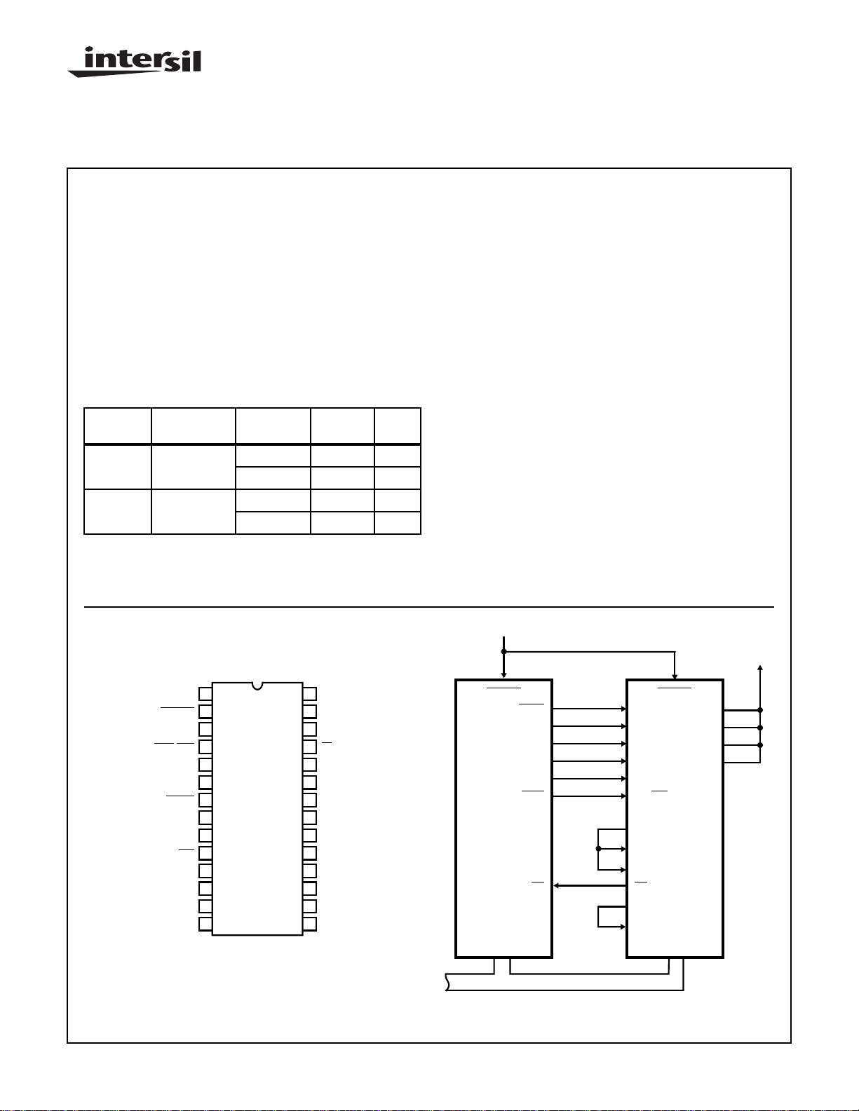
Ordering Information
PKG.
PACKAGE TEMP. RANGE 5V 10V
PDIP -40oC to +85oC CDP1855CE CDP1855E E28.6
Burn-In CDP1855CEX - E28.6
SBDIP -40oC to +85oC CDP1855CD CDP1855D D28.6
Burn-In CDP1855CDX - D28.6
NO.
Description
The CDP1855 and CDP1855C are CMOS 8-bit multiply/divide units which can be used to greatly increase the
capabilities of 8-bit microprocessors. They perform multiply
and divide operations on unsigned, binary operators. In
general, microprocessors do not contain multiply or divide
instructions and even efficiently coded multiply or divide
subroutines require considerable memory and execution
time. These multiply/divide units directly interface to the
CDP1800-series microprocessors via the N-lines and can
easily be configured to fit in either the memory or I/O space
of other 8-bit microprocessors.
The multiple/divide unit is based on a method of multiplying
by add and shift right operations and dividing by subtract and
shift left operations. The device is structured to permit cascading identical units to handle operands up to 32 bits.
The CDP1855 and CDP1855C are functionally identical.
They differ in that the CDP1855 has a recommended
operating voltage range of 4V to 10.5V, and the CDP1855C,
a recommended operating voltage range of 4V to 6.5V.
The CDP1855 and CDP1855C types are supplied in a 28
lead hermetic dual-in-line ceramic package (D suffix) and in
a 28 lead dual-in-line plastic package (E suffix). The
CDP1855C is also available in chip form (H suffix).
Pinout
CE
CLEAR
CTL
C.O./O.F.
Y
Z
SHIFT
CLK
STB
WE
RD/
RA2
RA1
RA0
V
SS
1
2
3
4
5
L
6
L
7
8
9
10
11
12
13
14
28 LEAD DIP
TOP VIEW
Circuit Configuration
+V
28
V
DD
27
CN0
CN1
26
CI
25
24
Y
R
Z
23
R
BUS 7
22
BUS 6
21
20
BUS 5
BUS 4
19
BUS 3
18
BUS 2
17
16
BUS 1
15
BUS 0
CLEAR
XTAL
N0
N1
N2
TPB
MRD
CDP1802
EF
BUS
FIGURE 1. MDU ADDRESSED AS I/O DEVICE
CLK
RA0
RA1
RA2
STB
RD/
Y
L
Z
R
CTL
C0
Y
R
Z
L
CLEAR
CE
C1
CN0
CN1
WE
CDP1855
BUS
CAUTION: These devices are sensitive to electrostatic discharge; follow proper IC Handling Procedures.
http://www.intersil.com or 407-727-9207
| Copyright © Intersil Corporation 1999
4-47
File Number 1053.2
Page 2
CDP1855, CDP1855C
Absolute Maximum Ratings Thermal Information
DC Supply Voltage Range, (VDD)
(All voltage values referenced to VSS terminal)
CDP1855 . . . . . . . . . . . . . . . . . . . . . . . . . . . . . . . . -0.5V to +11V
CDP1855C. . . . . . . . . . . . . . . . . . . . . . . . . . . . . . . . -0.5V to +7V
Input Voltage Range, All Inputs . . . . . . . . . . . . .-0.5V to VDD +0.5V
DC Input Current, Any One Input. . . . . . . . . . . . . . . . . . . . . . . . .±10mA
CAUTION: Stresses above those listed in “Absolute Maximum Ratings” may cause permanent damage to the device. This is a stress only rating and operation
of the device at these or any other conditions above those indicated in the operational sections of this specification is not implied.
Thermal Resistance (Typical) θJA (oC/W) θJC (oC/W)
PDIP Package. . . . . . . . . . . . . . . . . . . 55 N/A
SBDIP Package. . . . . . . . . . . . . . . . . . 50 12
Device Dissipation Per Output Transistor
For TA = Full Package-Temperature Range
(All Package Types). . . . . . . . . . . . . . . . . . . . . . . . . . . . . . 100mW
Operating Temperature Range (TA) . . . . . . . . . . . . .-40oC to +85oC
Storage Temperature Range (T
) . . . . . . . . . . . .-65oC to +150oC
STg
Lead Temperature (During Soldering)
At distance 1/16 ± 1/32 In. (1.59 ± 0.79mm)
from case for 10s max. . . . . . . . . . . . . . . . . . . . . . . . . . . . +265oC
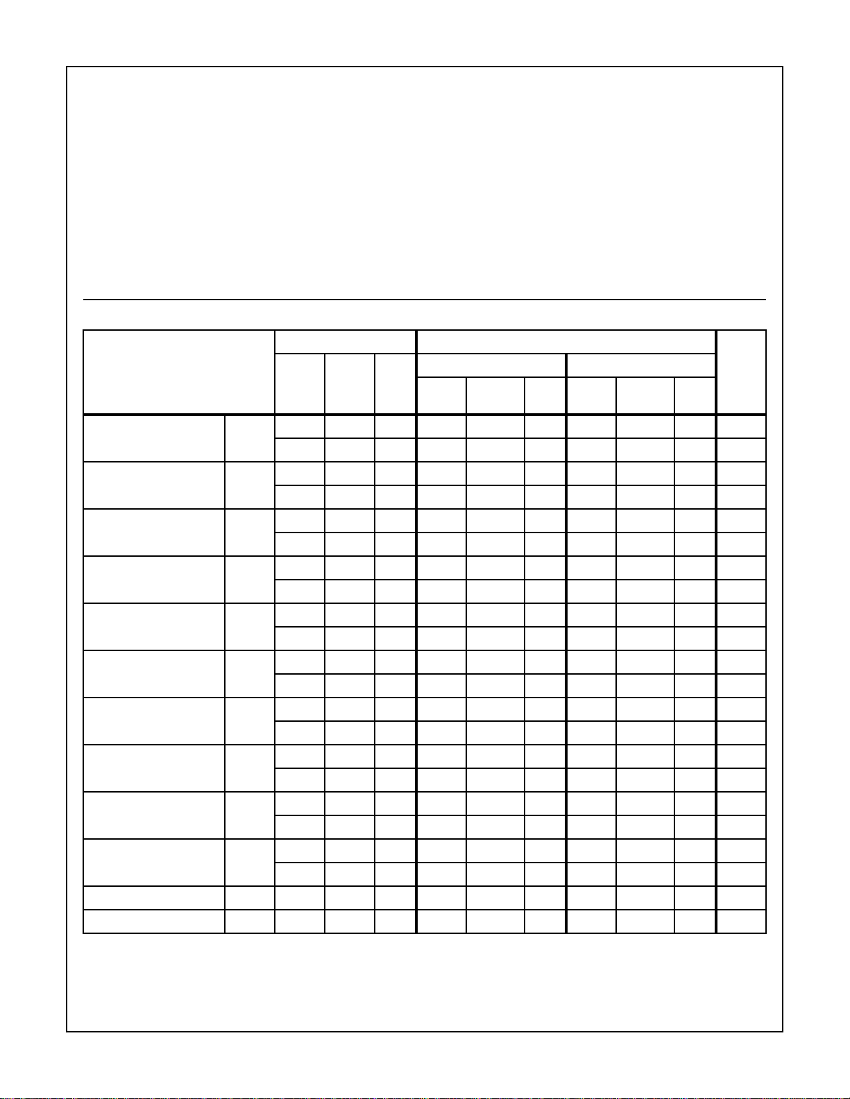
Static Electrical Specifications At T
= -40 to +85oC, VDD±10%, Unless Otherwise Specified
A
CONDITIONS LIMITS
PARAMETER
Quiescent Device
Current
Output Low Drive (Sink)
Current
Output High Drive
(Source) Current
Output Voltage Low Level
(Note 2)
Output Voltage High Level
(Note 2)
Input Low Voltage V
V
O
(V)
I
DD
- 0, 5 5 - 0.01 50 - 0.02 200 µA
- 0, 10 10 - 1 200 - - - µA
I
OL
0.4 0, 5 5 1.6 3.2 - 1.6 3.2 - mA
0.5 0, 10 10 2.6 5.2 - - - - mA
I
OH
4.6 0, 5 5 -1.15 -2.3 - -1.15 -2.3 - mA
9.5 0, 10 10 -2.6 -5.2 - - - - mA
V
OL
- 0, 5 5 - 0 0.1 - 0 0.1 V
- 0, 10 10 - 0 0.1 - - - V
V
OH
- 0, 5 5 4.9 5 - 4.9 5 - V
- 0, 10 10 9.9 10 - - - - V
0.5, 4.5 - 5 - - 1.5 - - 1.5 V
IL
V
(V)
IN
0.5, 9.5 - 10 - - 3 - - - V
Input High Voltage V
0.5, 4.5 - 5 3.5 - - 3.5 - - V
IH
0.5, 9.5 - 10 7 - - - - - V
Input Leakage Current I
IN
- 0, 5 5 - - ±1- - ±1 µA
- 0, 10 10 - - ±1- - -µA
Three-State Output
Leakage Current
Operating Current
(Note 3)
Input Capacitance C
Output Capacitance C
I
OUT
I
DD1
OUT
0, 5 0, 5 5 - - ±1- - ±1 µA
0, 10 0, 10 10 - - ±10 - - - µA
- 0, 5 5 - 1.5 - - 1.5 3 mA
- 0, 10 10 - 6 12 - - - mA
IN
- - - - 5 7.5 - 5 7.5 pF
- - - - 10 15 - 10 15 pF
NOTES:
1. Typical values are for TA = +25oC and nominal VDD.
2. IOL = IOH = 1µA
3. Operating current is measured at 3.2MHz with open outputs.
V
(V)
DD
CDP1855 CDP1855C
(NOTE1)
MIN
TYP MAX MIN
(NOTE1)
TYP MAX
UNITS
4-48
Page 3
CDP1855, CDP1855C
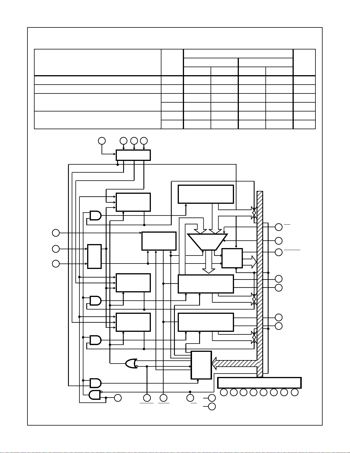
Recommended Operating Conditions At T
= Full package temperature range. For maximum reliability, operating conditions
A
should be selected so that operation is always within the following ranges:
LIMITS
CDP1855 CDP1855C
MIN MAX MIN MAX
UNITS
PARAMETER
V
DD
(V)
DC Operating Voltage Range - 4 10.5 4 6.5 V
Input Voltage Range - V
SS
V
DD
V
SS
V
DD
Maximum Clock Input Frequency 5 3.2 - 3.2 - MHz
10 6.4 - - - MHz
Minimum 8 x 8 Multiply (16 ÷ 8 Divide) Time 5 - 5.6 - 5.6 µs
10 - 2.8 - - µs
RA2 RA1 RA0CE
11
12 131
REGISTER
SELECT CONTROL
SELECT Z
SELECT Y
SELECT LOGIC
SELECT X
X SEQUENCE
COUNTER
RESET
OUT
SELECT STATUS
X REGISTER
LOAD
V
CLOCK
8
CN1
26
CN0
27
CHIP
NO.
8
SUBTRACT
Y REGISTER
RESET
Z REGISTER
RESET
CONTROL
LOAD
10729
ADD/
C.O.
8
REGISTER
14
V
V
28
BUS
22
SS
DD
7
STATUS
REG
8
8
BUS
6
21
Y SEQUENCE
COUNTER
RESET
Z SEQUENCE
COUNTER
RESET
SHIFT
GENERATOR
OUT
OUT
8
SHIFT
LOAD
SHIFT
LOAD
RD/WESHIFTCLEARSTB
FIGURE 2. BLOCK DIAGRAM OF CDP1855 AND CDP1855C
BUS
5
20
BUS
4
19
BUS
3
18
BUS
2
17
25
3
4
5
24
6
23
BUS
C.I.
CTL.
C.O./O.F.
Y
L
Y
R
Z
L
Z
R
BUS
1
16
0
15
4-49
Page 4

Functional Description
CDP1855, CDP1855C
The CDP1855 is a multiply-divide unit (MDU) designed to be
compatible with CDP1800 series microprocessor systems. It
can, in fact, be interfaced to most 8-bit microprocessors (see
Figure 5). The CDP1855 performs binary multiply or divide
operations as directed by the microprocessor. It can do a
16N-bit by 8N-bit divide yielding a 8N-bit result plus and 8Nbit remainder. The multiply is an 8N-bit by 8N-bit operation
with a 16N-bit result. The “N” represent the number of
cascaded CDP1855's and can be 1, 2, 3 or 4. All operations
require 8N + 1 shift pulses (See “DELAY NEEDED WITH
AND WITHOUT PRESCALER”).
The CDP1855 contains three registers, X, Y, and Z, which
are loaded with the operands prior to an operation and
contain the results at the completion. In addition, the control
register must be loaded to initiate a multiply or divide. There
is also a status register which contains an overflow flag as
shown in the “CONTROL REGISTER BIT ASSIGNMENT
TABLE”. The register address lines (RA0-RA1) are used to
select the appropriate register for loading or reading. The
RD/
WE and STB lines are used in conjunction with the RA
lines to determine the exact MDU response (See
“CONTROL TRUTH TABLE”).
When multiple MDU's are cascaded, the loading of each register is done sequentially. For example, the first selection of
register X for loading loads the most significant CDP1855,
the second loads the next significant, and so on. Registers
are also read out sequentially. This is accomplished by internal counters on each MDU which are decremented by STB
during each register selection. When the counter matches
the chip number (CN1, CN0 lines), the device is selected.
These counters must be cleared with a clear on pin 2 or with
bit 6 in the control word (See “CONTROL REGISTER BIT
ASSIGNMENT TABLE”) in order to star t each sequence of
accesses with the most significant device.
The CDP1855 has a built in clock prescaler which can be
selected via bit 7 in the control register. The prescaler may
be necessary in cascaded systems operating at high
frequencies or in systems where a suitable clock frequency
is not readily available. Without the prescaler select, the shift
frequency is equal to the clock input frequency. With the
prescaler selected, the rate depends on the number of
MDU's as defined by bits 4 and 5 of the control word (See
“CONTROL REGISTER BIT ASSIGNMENT TABLE”).
1. For one MDU, the clock frequency is divided by 2.
2. For two MDU's the clock frequency is divided by 4.
3. For 3 or 4 MDU's, the clock frequency is divided by 8.
Operation
1. Initialization and Controls
The CDP1855 must be cleared by a low on pin 2 during
power-on which prevents bus contention problems at the Y
Y
and ZL, ZR terminals and also resets the sequence
R
counters and the shift pulse generator.
Prior to loading any other registers the control register must
be loaded to specify the number of MDU's being used (See
“CONTROL REGISTER BIT ASSIGNMENT TABLE”).
Once the number of devices has been specified and the
sequence counters cleared with a clear pulse or bit 6 of the
control word, the X, Y, and Z registers can be loaded as
defined in the “CONTROL TRUTH TABLE”. All bytes of the X
register can be loaded, then all bytes of the Y, and then all
bytes of the Z, or they can be loaded randomly. Successive
loads to a given register will always proceed sequentially
from the most significant byte to the least significant byte, as
previously described. Resetting the sequence counters
select the most significant MDU. In a four MDU system, loading all MDU's results in the sequence counter pointing to the
first MDU again. In all other configurations (1, 2, or 3
MDU's), the sequence counter must be reset prior to each
series of register reads or writes.
2. Divide Operation
For the divide operation, the divisor is loaded in the X
register. The dividend is loaded in the Y and Z registers with
the more significant half in the Y register and the less significant half in the Z register. These registers may be loaded in
any order, and after loading is completed, a control word is
loaded to specify a divide operation and the number of
MDU's and also to reset the sequence counters and Y or Z
register and select the clock option if desired. Clearing the
sequence counters with bit 6 will set the MDU's up for reading the results.
The X register will be unaltered by the operation. The
quotient will be in the Z register while the remainder will be in
the Y register. An overflow will be indicated by the
of the most significant MDU and can also be determined by
reading the status byte.
While the CDP1855 is specified to perform 16 by 8-bit
divides, if the quotient of a divide operation exceeds the size
of the Z register(s) (8N-bits - where N is the number of
cascaded CDP1855's) the overflow bit in the Status Register
will be set. Neither the quotient in Z nor the remainder in Y
will represent a valid answer. This will always be the result of
a division performed when the divisor (X) is equal to or less
than the most significant 8N-bits of the dividend (Y).
The MDU can still be used for such computations if the
divide is done in two steps. The dividend is split into two
parts-the more significant 8N-bits and the less significant
8N-bits-and a divide done on each part. Each step yields an
8N-bit result for a total quotient of 16N-bits.
The first step consists of dividing the more significant 8Nbits by the divisor. This is done by clearing the Y register(s),
loading the Z register(s) with the more significant 8N-bits of
the dividend, and loading the X register(s) with the divisor. A
division is performed and the resultant value in Z represents
,
L
the more significant 8N-bits of the final quotient. The Z register(s) value must be unloaded and saved by the processor.
C.O./O.F.
4-50
Page 5

CDP1855, CDP1855C
A second division is performed using the remainder from the
first division (in Y) as the more significant 8N-bits of the dividend and the less significant half of the original dividend
loaded into the Z register. The divisor in X remains unaltered
and is, by definition, larger than the remainder from the first
division which is in Y. The resulting value in Z becomes the
less significant 8N-bits of the final quotient and the value in Y
is, as usual, the remainder.
Extending this technique to more steps allows division of any
size number by an 8N-bit divisor.
Note that division by zero is never permitted and must be
tested for and handled in software.
The following example illustrates the use of this algorithm.
Example:
Assume three MDU's capable of a by 24-bit division. The
problem is to divide 00F273, 491C06H by 0003B4H.
Step 1: 000000 , 00F273 / 0003B4 = 000041 R=0001BF
Y Z(MS) X Z1 Y1
Step 2: 0001BF , 491C06 / 0003B4 = 78C936 R=00000E
Y1 Z(LS) X Z2 Y2
Result: 000041 , 78C936 R=00000E
Z1 Z2 Y2
The Z register can simply be reset using bit 2 of the control
word and another divide can be done in order to further
divide the remainder.
3. Multiply Operation
For a multiply operation the two numbers to be m ultiplied are
loaded in the X and Z registers. The result is in the Y and Z
register with Y being the more significant half and Z the less
significant half. The X register will be unchanged after the
operation is completed.
The original contents of the Y register are added to the
product of X and Z. Bit 3 of the control word will reset
register Y to 0 if desired.
Functional Description of
CDP1855 Terminals
CE - Chip Enable (Input):
ZR of the least significant CDP1855 MDU. This signal is
used to indicate whether the registers are to be operated on
or only shifted.
C.O./O.F. - Carry Out/Over Flow (Output):
This is a three-state output pin. It is the CDP1855
signal and is connected to
Cl (CARRY-IN) of the next more
Carry Out
significant CDP1855 MDU, except for on the most significant
MDU. On that MDU it is an overflow indicator and is enabled
when chip enables is true. A low on this pin indicates that an
overflow has occurred. The overflow signal is latched each
time the control register is loaded, but is only meaningful
after a divide command.
Y
, YR - Y-Left, Y-Right:
L
These are three-state bi-directional pins for data transfer
between the Y registers of cascaded CDP1855 MDU's. The
Y
pin is an output and YL is an input during a multiply and
R
the reverse is true at all other times. The Y
connected to the Y
An exception is that the Y
pin of the next more significant MDU.
R
pin of the most significant
L
CDP1855 MDU must be connected to the Z
pin must be
L
pin of the least
R
significant MDU and to the CTL pins of all MDU's. Also the
Y
pin of the least significant MDU is tied to the ZL pin of the
R
most significant MDU.
Z
, ZR - Z-Left, Z-Right:
L
These are three-state bi-directional pins for data transfers
between the “Z” registers of cascaded MDU's. The Z
an output and Z
reverse is true at all other times. The Z
the Y
pin of the next more significant MDU. An exception is
R
that the Z
L
nected to the Y
Z
pin of the least significant MDU is tied to the YL of the
R
is an input during a multiply and the
L
pin must be tied to
L
in of the most significant MDU must be con-
pin of the least significant MDU. Also, the
R
pin is
R
most significant MDU.
Shift - Shift Clock:
This is a three-state bi-directional pin. It is an output on the
most significant MDU. And an input on all other MDU's. It
provides the MDU system timing pulses. All
SHIFT pins must
be connected together for cascaded operation. A maximum
of the 8N +1 shifts are required for an operation where "N"
equals the number of MDU devices that are cascaded.
A high on this pin enables the CDP1855 MDU to respond to
the select lines. All cascaded MDU's must be enabled
together. CE also controls the three-state
C.O./O.F., output
of the most significant MDU.
Clear (Input):
The CDP1855 MDU(s) must be cleared upon power-on with
a low-on this pin. The clear signal resets the sequence
counters, the shift pulse generator, and bits 0 and 1 of the
control register.
CTL - Control (Input):
This is an input pin. All CTL pins must be wired together and
to the Y
of the most significant CDP1855 MDU and to the
L
CLK - Clock (Input):
This pin should be grounded on all but the most significant
MDU. There is an optional reduction of clock frequency a v ailable on this pin if so desired, controlled by bit 7 of the control
byte.
STB - Strobe (Input):
When RD/WE is low, data is latched from bus lines on the
falling edge of this signal. It may be asynchronous to the
clock. Strobe also increments the selected register's
sequence counter during reads and writes. TPB would be
used in CDP1800 systems.
4-51
Page 6

CDP1855, CDP1855C
RD/WE - Read/Write Enable (Input):
This signal defines whether the selected register is to be
read from or written to. In 1800 systems use
are addressed as I/O devices,
MWR is used if MDU's are
MRD if MDU's
addressed as memory devices.
RA2, RA1, RA0 - Register Address (Input):
These input signals define which register is to be read from
Y
- Y-Right:
R
See Pin 5.
Cl- Carry In (Input):
This is an input for the carry from the next less significant
MDU. On the least significant MDU it must be high (V
all others it must be connected to the
significant MDU.
or written to. It can be seen in the “CONTROL TRUTH
TABLE” that RA2 can be used as a chip enable. It is identical
to the CE pin, except only CE controls the three-state
C.O./O.F. on the most significant MDU. In 1800 systems use
N lines if MDU's are used as I/O devices, use address lines
or function of address lines if MDU's are used as memory
devices.
Bus 0 - Bus 7 - Bus Lines:
Three-state bi-directional bus for direct interface with
CDP1800 series and other 8-bit microprocessors.
Z
- Z-Right:
R
See Pin 6.
CONTROL TRUTH TABLE
INPUTS (NOTE 1)
RA2
(N2)
0XXXXXNo Action (Bus Floats)
X0XXXXNo Action (Bus Floats)
11001XX to Bus
11011XZ to Bus
11101XY to Bus
11111XStatus to Bus
110001Load X from Bus
110101Load Z from Bus
111001Load Y from Bus
111101Load Control Register
1 1 X X 0 0 No Action (Bus Floats)
NOTE:
1. ( ) = 1800 System Signals. 1 = High Level, 0 = Low Level, X = High or Low Level.
RA1
(N1)
RA0
(N0)
RD/WE
(MRD)
CN1, CN0 - Chip Number (Input):
These two input pins are wired high or low to indicate the
MDU position in the cascaded chain. Both are high for the
most significant MDU regardless of how many CDP1855
MDU's are used. Then CN1 = high and CN0 = low for the
next MDU and so forth.
V
- Ground:
SS
Power supply line.
V
- V+:
DD
Power supply line.
STB
(TPB)
CO pin of the next less
RESPONSECE
Increment Sequence
Counter When STB
and RD = 1
Increment Sequence
Counter
DD
) on
4-52
Page 7

CDP1855, CDP1855C
CONTROL REGISTER BIT ASSIGNMENT TABLE
BUS 7 BUS 6 BUS 5 BUS 4 BUS 3 BUS 2 BUS 1 BUS 0
B1 B0 OPERATION SELECT
REGISTER
RESET
B2 = 1, RESET Z REGISTER
B3 = 1, RESET Y REGISTER
B5 B4 NO. OF MDU’s
1 1 One MDU
1 0 Two MDU’s
0 1 Three MDU’s
0 0 Four MDU’s
B6 = 1, RESET SEQUENCE COUNTER 2 Clock ÷ 4
B7 = 1, SELECT SHIFT RATE OPTIONS:
B7 = 0, SHIFT = CLOCK FREQUENCY RATE
0 0 No Operation
0 1 Multiply
1 0 Divide
1 1 Illegal State
NO. OF MDU’s SHIFT RATE
1 Clock ÷ 2
3 Clock ÷ 8
4 Clock ÷ 8
BIT 76543210
OUTPUT 0000000O.F.
NOTES:
1. O.F. = 1 if overflow (only valid after a divide has been done)
2. Bits 1 - 7 are read as 0 always.
DELAY NEEDED WITH AND WITHOUT PRESCALER
8N + 1 Shifts/Operation at 1 Clock Cycle/Shift
N = Number of MDU’s, S = Shift Rate
WITHOUT PRESCALER WITH PRESCALER
SHIFTS = 8N +1
NO. OF MDU’s
1 9 2 (1 NOP) 18 3 (1 NOP) 2
2 17 2 (1 NOP) 68 9 (3 NOPs) 4
3 25 3 (1 NOP) 200 25 (9 NOPs) 8
4 33 4 (2 NOPs) 264 33 (11 NOPs) 8
NEEDED
STATUS REGISTER
(NOTE 1)
MACHINE CYCLES
NEEDED
STATUS BYTE
SHIFTS = S (8N +1)
NEEDED
(NOTE 1)
MACHINE CYCLES
NEEDED SHIFT RATE
NOTE:
1. NOP instruction is shown for machine cycles needed (3/NOP). Other instructions may be used.
4-53
Page 8

CDP1855, CDP1855C
CDP1855 Interfacing Schemes
CN0
CN1
CTL
+V
CI
Y
L
Z
R
Y
R
Z
L
CLEAR
CDP1802
BUS
XTAL
MA0
MA1
MAX
TPA
MWR
MRD
TPB
EF
HIGH
ADDRESS
LATCH
CLEAR
CLOCK
RA0
RA1
RA2
CDP1855
RE/WE
CE
STB
CO
BUS
FIGURE 3. REQUIRED CONNECTION FOR MEMORY MAPPED
ADDRESSING OF THE MDU
DD
V
CC
2526272814
CI
V
DD
SS
CDP1855
2
CLEAR
8
CLK
10
WE
RD/
9
STB
CN1CN0V
MDU
1/4 CD4011
1/4 CD4011
CERA0RA1RA2
1131211
Y
Z
CTL
Y
Z
BUS 7
BUS 6
BUS 5
BUS 4
BUS 3
BUS 2
BUS 1
BUS 0
24
R
6
L
3
5
L
23
R
22
21
20
19
18
17
16
15
DATA BUS
A8
A9
IO/
M
WR
RD
CLK (OUT)
RESET OUT
DATA
BUS
FIGURE 4. INTERFACING THE CDP1855 TO AN 8085 MICRO-
PROCESSOR AS AN I/O DEVICE
8085 SIGNAL
Programming Example for Multiplication
For a 24-bit x 24-bit multiply using the system shown in Figure 5, the following is an assembly listing of a program to multiply 201F7C16 by
723C0916:
MEMORY
LOCATION
0000 F830; 0001 LDI 030H
0002 A2; 0002 PLO R2 . . LOAD 30 INTO R2.0
0003 F800; 0003 LDI 00H
0005 B2; 0004 PHI R2 . . LOAD 00 INTO R2.1 (R2=0030)
0006 6758; 0005 OUT 7; DC 058H . . LOAD CONTROL REGISTERS
0008 ; 0006 . . SPECIFYING THREE MDU’s
0008 ; 0007 . . RESET THE Y REGISTER AND
0008 ; 0008 . . SEQUENCE COUNTER
0008 6420; 0009 OUT 4; DC 020H . . LOAD MSB OF X REGISTER
000A ; 0010 . . WITH 20
000A 641F; 0011 OUT 4; DC 01FH . . LOAD NEXT MSB OF X REG
000C ; 0012 . . WITH 1F
000C 647C; 0013 OUT 4; DC 07CH . . LOAD LSB OF X REGISTER
000E ; 0014 . . WITH 7C
000E 6572; 0015 OUT 5; DC 072H . . LOAD MSB OF Z REGISTER
0010 ; 0016 . . WITH 72
OP
CODE
LINE
NO. ASSEMBLY LANGUAGE
4-54
Page 9

CDP1855, CDP1855C
Programming Example for Multiplication
For a 24-bit x 24-bit multiply using the system shown in Figure 5, the following is an assembly listing of a program to multiply 201F7C16 by
723C0916: (Continued)
MEMORY
LOCATION
0010 653C; 0017 OUT 5; DC 030H . . LOAD NEXT MSB OF Z REG
0012 ; 0018 . . WITH 3C
0012 6509; 0019 OUT 5; DC 09H . . LOAD LSB OF Z REGISTER
0014 ; 0020 . . WITH 09
0014 6759; 0021 OUT 7; DC 059H . . LOAD CONTROL REGISTERS
0016 ; 0022 . . RESETTING Y REGISTERS
0016 ; 0023 . . AND SEQUENCE COUNTERS
0016 ; 0024 . . AND STARTING MULTIPLY
0016 ; 0025 . . OPERATION
DELAY FOR MULTIPLY TO FINISH
0016 E2; 0026 SEX R2
0017 6E60; 0027 INP 6; IRX . . MSB OF RESULTS IS STORED
0019 ; 0028 . . AT LOCATION 0030
0019 6E60; 0029 INP 6; IRX
001B 6E60; 0030 INP 6; IRX
001D 6D60; 0031 INP 5; IRX
001F 6D60; 0032 INP 5; IRX
0021 6D; 0033 INP 5 . . COMPLETE LOADING RESULT
0022 ; 0034 . . INTO MEMORY LOCATIONS
0022 ; 0035 . . 0030 TO 0035
0022 ; 0036 . . RESULTS = 0E558DBA2B5C
0022 3022; 0037 STOP BR STOP
0024 ; 0038 END
0000
OP
CODE
LINE
NO. ASSEMBLY LANGUAGE
The result of 201F7C
15760612797276
. It will be stored in memory as follows:
10
LOC BYTE
0030 0E
31 55
32 8D
33 BA
34 2B
35 5C
x 723C0916 is 0E558DBA2B5C =
16
BEFORE MULTIPLY
MDU1 MDU2 MDU3
REGISTER X 20 1F 7C
REGISTER Y 00 00 00
REGISTER Z 72 3C 09
AFTER MULTIPLY
MDU1 MDU2 MDU3
REGISTER X 20 1F 7C
REGISTER Y 0E 55 8D
REGISTER Z BA 2B 5C
4-55
Page 10

CDP1855, CDP1855C
Programming Example for Division
MEMORY
LOCATION
0000 ; 0001 . . Program example for a 16-bit by 8-bit divide using 1 CDP1855 MDU
0000 ; 0002 . . Gives a 16-bit answer with 8-bit remainder
0000 ; 0003
0000 68C22000; 0004 RLDI R2, 2000H . . Answer is stored at 2000 hex
0004 ; 0005 . . Register 2 points to it
0004 68C33000; 0006 RLDI R3, 3000H . . Dividend is stored at 3000 hex
0008 ; 0007 . . Register 3 points to it
0008 68C44000; 0008 RLDI R4, 4000H . . Divisor is stored at 4000 hex
000C ; 0009 . . Register 4 points to it
000C ; 0010
000C E067F0; 0011 SEX R4; OUT 7; DC OF0H . . Write to the control register to use
000F ; 0012 . . clock/2; 1MDU; reset sequence
000F ; 0013 . . counter; and no operation
000F ; 0014
000F E464; 0015 SEX R4; OUT 4 . . Load the divisor into the X register
0011 ; 0016
0011 E06600; 0017 SEX R0; OUT 6; DC 0 . . Load 0 into the Y register
0014 E365; 0018 SEX R3; OUT 5 . . Load the most significant 8 bits of
0016 ; 0019 . . the dividend into the Z register
0016 ; 0020
0016 E067F2; 0021 SEX R0; OUT 7; DC 0F2H . . Do the first divide, also resets the
0019 ; 0022 . . sequence counter
0019 ; 0023
0019 E26D60; 0024 SEX R2; INP 5; IRX . . Read and store the most significant
001C ; 0025 . . 8 bits of the answer at 2000 hex
001C ; 0026
001C E067F0; 0027 SEX R0; OUT 7; DC 0F0H . . Reset the sequence counter
001F ; 0028
001F E365; 0029 SEX R3; OUT 5 . . Load the 8 least significant 8 bits
0021 ; 0030 . . of the original dividend into the Z
0021 ; 0031 . . register
0021 ; 0032
0021 E067F2; 0033 SEX R0; OUT 7; DC 0F2H . . Do the second division
0024 ; 0034
0024 E26D60; 0035 SEX R2; INP 5; IRX . . Read and store the least significant
0027 ; 0036 . . 8 bits of the answer at 2001 hex
0027 6E; 0037 INP 6 . . Read and store the remainder at 2002
0028 ; 0038 . . hex
0000
OP
CODE
LINE
NO. ASSEMBLY LANGUAGE
For the divide operation (Figure 5), the formula is:
4-56
Page 11

CDP1855, CDP1855C
Y3Y2Y1Z3Z2Z
------------------------------------------- - Z3Z2Z
X3X2X
1
=
1
1
Y
3Y2Y1
--------------------- -+
X3X2X
1
EF1
DATA BUS
8
BUS
MRD
TPB
CLEAR
N2
N1
N0
V
DD
OR
I/O SELECT
CLOCK
V
DD
888
CLRSTBRD/BUS
RA0
RA1
RA2
C.I.
Y
R
Z
R
CN1
CN0
CLK
SHIFT
Y
L
Z
L
O.F.
WE
CDP1855
CTLCE
V
DD
CN1
CN0
CLK
SHIFT
Y
L
Z
L
C.O.
WE
CDP1855
CLRSTBRD/BUS
RA0
RA1
RA2
C.I.
Y
R
Z
R
CTLCE
V
DD
CN1
CN0
CLK
SHIFT
Y
L
Z
L
C.O.
WE
CDP1855
CLRSTBRD/BUS
RA0
RA1
RA2
C.I.
V
DD
Y
R
Z
R
CTLCE
MOST SIGNIFICANT LEAST SIGNIFICANT
FIGURE 5. CASCADING THREE MDU’s (CDP1855) IN AN 1800 SYSTEM WITH MDU’s BEING ACCESSED AS I/O PORTS IN
PROGRAMMING EXAMPLE
TO
CPU
DATA BUS
V
DD
CN1
CN0
CLK
SHIFT
Y
L
Z
L
O.F.
WE
CDP1855
CLRSTBRD/BUS
RA0
RA1
RA2
C.I.
Y
R
Z
R
CTLCE
V
DD
CN1
CN0
CLK
SHIFT
Y
L
Z
L
C.O.
WE
CDP1855
CLRSTBRD/BUS
RA0
RA1
RA2
C.I.
Y
R
Z
R
CTLCE
V
DD
CN1
CN0
CLK
SHIFT
Y
L
Z
L
C.O.
WE
CDP1855
CLRSTBRD/BUS
RA0
RA1
RA2
C.I.
CN1
CN0
CLK
SHIFT
Y
R
Z
R
Y
L
Z
L
C.O.
CTLCE
MOST SIGNIFICANT LEAST SIGNIFICANT
FIGURE 6. CASCADING FOUR MDU’s (CDP1855)
WE
CDP1855
CTLCE
CLRSTBRD/BUS
RA0
RA1
RA2
C.I.
CLOCK
EF1
BUS
MRD
TPB
CLEAR
N2
N1
N0
V
DD
Y
R
Z
R
4-57
Page 12

CDP1855, CDP1855C
Dynamic Electrical Specifications At T
CL = 100pF (See Figure 7)
(NOTE 1)
PARAMETER
OPERATION TIMING
Maximum Clock Frequency
(Note 3)
Maximum Shift Frequency
(1 Device) (Note 4)
Minimum Clock Width t
Minimum Clock Period t
Clock to Shift Propagation
Delay
CLK0
t
CLK1
CLK
t
CSH
V
DD
(V)
5 3.2 4 - 3.2 4 - MHz
10 6.4 8 - - - - MHz
5 1.6 2 - 1.6 2 - MHz
10 3.2 4 - - - - MHz
5 - 100 150 - 100 150 ns
10 - 50 75 - - - ns
5 - 250 312 - 250 312 ns
10 - 125 156 - - - ns
5 - 200 300 - 200 300 ns
10 - 100 150 - - - ns
= -40 to +85oC, VDD±5%, tR, tF = 20ns, VIH = 0.7VDD, VIL = 0.3VDD,
A
LIMITS
CDP1855 CDP1855C
MIN
(NOTE 2)
TYP MAX MIN
(NOTE 2)
TYP MAX
UNITS
Minimum C.I. to Shift Setup t
SU
5 - 50 67 - 50 67 ns
10 - 25 33 - - - ns
C.O. from Shift Propagation
Delay
Minimum C.I. from Shift Hold t
t
PLH
t
PHL
5 - 450 600 - 450 600 ns
10 - 225 300 - - - ns
H
5 - 50 75 - 50 75 ns
10 - 25 40 - - - ns
Minimum Register Input
t
SU
5 - -20 10 - -20 10 ns
Setup
10 - -10 10 - - - ns
Register after Shift Delay t
Minimum Register after Shift
PLH
t
PHL
t
H
5 - 400 600 - 400 600 ns
10 - 200 300 - - - ns
5 - 50 100 - 50 100 ns
Hold
10 - 25 50 - - - ns
C.O. from C.I. Propagation
Delay
Register from C.I.
Propagation Delay
t
PLH
t
PHL
t
PLH
t
PHL
5 - 100 150 - 100 150 ns
10 - 50 75 - - - ns
5 - 80 120 - 80 120 ns
10 - 40 60 - - - ns
NOTES:
1. Maximum limits of minimum characteristics are the values above which all devices function.
2. Typical values are for TA = 25oC and nominal voltages.
3. Clock frequency and pulse width are given for systems using the internal clock option of the CDP1855. Clock frequency equals shift
frequency for systems not using the internal clock option.
4. Shift period for cascading of devices is increased by an amount equal to the C.I. to C.O. Propagation Delay for each device added.
4-58
Page 13

CDP1855, CDP1855C
Dynamic Electrical Specifications At T
= -40 to +85oC, VDD±5%, tR, tF = 20ns, VIH = 0.7VDD, VIL = 0.3VDD,
A
CL = 100pF (See Figure 8)
LIMITS
CDP1855 CDP1855C
(NOTE 1)
PARAMETER
V
DD
(V)
MIN
(NOTE 2)
TYP MAX MIN
WRITE CYCLE
Minimum Clear Pulse Width t
CLR
5 - 50 75 - 50 75 ns
10 - 25 40 - - - ns
Minimum Write Pulse Width t
WW
5 - 150 225 - 150 225 ns
10 - 75 115 - - - ns
Minimum Data-In-Setup t
DSU
5 - -75 0 - -75 0 ns
10 - -40 0 - - - ns
Minimum Data-In-Hold t
DH
5 - 50 75 - 50 75 ns
10 - 25 40 - - - ns
Minimum Address to Write
Setup
Minimum Address after
Write Hold
t
ASU
t
AH
5 - 50 75 - 50 75 ns
10 - 25 40 - - - ns
5 - 50 75 - 50 75 ns
10 - 25 40 - - - ns
NOTES:
1. Maximum limits of minimum characteristics are the values above which all devices function.
2. Typical values are for TA = 25oC and nominal voltages.
Dynamic Electrical Specifications At T
= -40 to +85oC, VDD±5%, tR, tF = 20ns, VIH = 0.7VDD, VIL = 0.3VDD,
A
CL = 100pF (See Figure 9)
LIMITS
CDP1855 CDP1855C
(NOTE 1)
PARAMETER
V
DD
(V)
MIN
(NOTE 2)
TYP MAX MIN
READ CYCLE
CE to Data Out Active t
CDO
5 - 200 300 - 200 300 ns
10 - 100 150 - - - ns
CE to Data Access t
CA
5 - 300 450 - 300 450 ns
10 - 150 225 - - - ns
Address to Data Access t
AA
5 - 300 450 - 300 450 ns
10 - 150 225 - - - ns
Data Out Hold after CE t
DOH
5 50 150 225 50 150 225 ns
10 25 75 115 - - - ns
Data Out Hold after Read t
DOH
5 50 150 225 50 150 225 ns
10 25 75 115 - - - ns
Read to Data Out Active t
RDO
5 - 200 300 - 200 300 ns
10 - 100 150 - - - ns
Read to Data Access t
RA
5 - 200 300 - 200 300 ns
10 - 100 150 - - - ns
(NOTE 2)
TYP MAX
(NOTE 2)
TYP MAX
UNITS
UNITS
4-59
Page 14

CDP1855, CDP1855C
Dynamic Electrical Specifications At T
= -40 to +85oC, VDD±5%, tR, tF = 20ns, VIH = 0.7VDD, VIL = 0.3VDD,
A
CL = 100pF (See Figure 9) (Continued)
LIMITS
CDP1855 CDP1855C
(NOTE 1)
PARAMETER
Strobe to Data Access t
SA
V
DD
(V)
MIN
(NOTE 2)
TYP MAX MIN
5 50 200 300 50 200 300 ns
10 25 100 150 - - - ns
Minimum Strobe Width t
SW
5 - 150 225 - 150 225 ns
10 - 75 115 - - - ns
NOTES:
1. Maximum limits of minimum characteristics are the values above which all devices function.
2. Typical values are for TA = 25oC and nominal voltages.
Timing Diagrams
t
CLOCK
CLK
(PRESCALER OFF)
SHIFT
t
CLK 1
t
CLK 0
t
CSH
12 9
12 9
t
, t
PLH
PHL
(NOTE 2)
TYP MAX
UNITS
C.O., YL, YR, ZL, ZR OUT
CIN, YL, YR, ZL, ZR IN
CLEAR
CE
RD/
WE
STB
D
RA0-2
t
SU
t
H
FIGURE 7. OPERATION TIMING DIAGRAM
t
CLR
* t
WW
IN
t
DSU
t
ASU
* WRITE IS OVERLAP OF CE = 1, RD/WE = 0, AND STB = 1.
t
DH
t
AH
FIGURE 8. WRITE TIMING DIAGRAM
4-60
Page 15

CDP1855, CDP1855C
Timing Diagrams
CE
RD/
WE
STB
RA0-2
D
OUT
(Continued)
t
CDO
ADVANCE
SEQUENCE COUNTER
t
SW
t
t
SA
t
CA
AA
FIGURE 9. READ TIMING DIAGRAM
t
DOH
t
RDO
t
DOH
t
RA
All Intersil semiconductor products are manufactured, assembled and tested under ISO9000 quality systems certification.
Intersil products are sold by description only. Intersil Corporation reserves the right to make changes in circuit design and/or specifications at any time without
notice. Accordingly, the reader is cautioned to verify that data sheets are current before placing orders. Information furnished by Intersil is believed to be accurate
and reliable. However, no responsibility is assumed by Intersil or its subsidiaries for its use; nor for any infringements of patents or other rights of third parties which
may result from its use. No license is granted by implication or otherwise under an y patent or patent rights of Intersil or its subsidiaries.
For information regarding Intersil Corporation and its products, see web site http://www.intersil.com
Sales Office Headquarters
NORTH AMERICA
Intersil Corporation
P. O. Box 883, Mail Stop 53-204
Melbourne, FL 32902
TEL: (407) 724-7000
FAX: (407) 724-7240
EUROPE
Intersil SA
Mercure Center
100, Rue de la Fusee
1130 Brussels, Belgium
TEL: (32) 2.724.2111
FAX: (32) 2.724.22.05
4-61
ASIA
Intersil (Taiwan) Ltd.
Taiwan Limited
7F-6, No. 101 Fu Hsing North Road
Taipei, Taiwan
Republic of China
TEL: (886) 2 2716 9310
FAX: (886) 2 2715 3029
 Loading...