

Page 1
March 1997
CDP1854A/3,
CDP1854AC/3
High Reliability CMOS Programmable Universal
Asynchronous Receiver/Transmitter (UART)
Features
• Two Operating Modes
- Mode 0 - Functionally Compatible with Industry
Types Such as the TR1602A and CDP6402
- Mode 1 - Interfaces Directly with CDP1800 Series
Microprocessors without Additional Components
• Full or Half-Duplex Operation
• Parity, Framing, and Overrun Error Detection
• Fully Programmable with Externally Selectable Word
Length (5-8 Bits), Parity Inhibit, Even/Odd Parity, and
1, 1-1/2, or 2 Stop Bits
Ordering Information
PACK-
AGE
SBDIP -55oC to +125oC CDP1854ACD3 CDP1854ACD3 D40.6
TEMP.
RANGE
5V/200K
BAUD
10V/400K
BAUD
PKG.
NO.
Description
The CDP1854A/3 and CDP1854AC/3 are high reliability
silicon gate CMOS Universal Asynchronous Receiver/Transmitter (UART) circuits. They are designed to provide the
necessary formatting and control for interfacing between
serial and parallel data. For example, these UARTs can be
used to interface between a peripheral or terminal with serial
I/O ports and the 8-bit CDP1800-series microprocessor
parallel data bus system. The CDP1854A/3 is capable of full
duplex operation, i.e., simultaneous conversion of serial
input data to parallel output data and parallel input data to
serial output data.
The CDP1854A/3 UART can be programmed to operate in
one of two modes by using the mode control input. When the
mode input is high (MODE = 1), the CDP1854A/3 is directly
compatible with the CDP1800 series microprocessor system
without additional interface circuitry. When the mode input is
low (MODE = 0), the device is functionally compatible with
industry standard UARTs such as the TR1602A and
CDP6402. It is also pin compatible with these types, except
that pin 2 is used for the mode control input.
The CDP1854A/3 and the CDP1854AC/3 are functionally
identical. The CDP1854A/3 has a recommended operating
voltage range of 4V to 10.5V, and the CDP1854AC/3 has a
recommended operating voltage range of 4V to 6.5V.
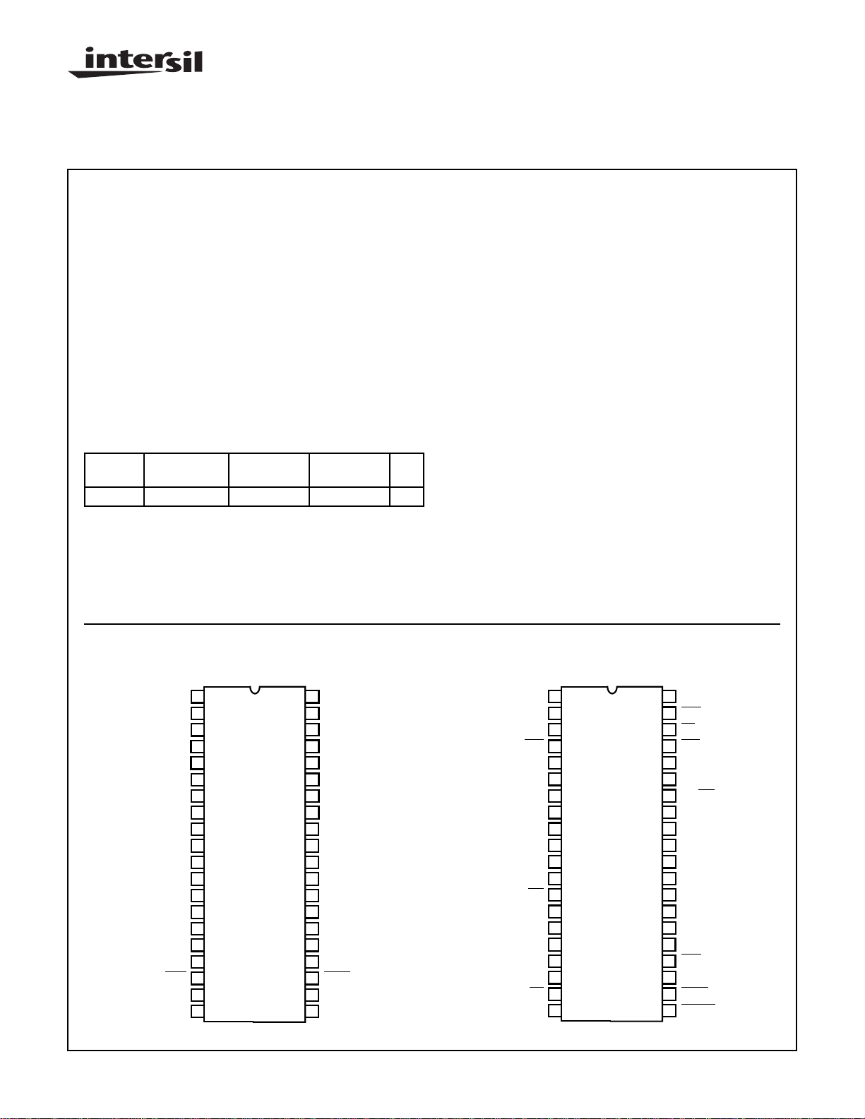
Pinouts
CDP1854A/3, CDP1854AC/3 (SBDIP) (MODE 0)
MODE (V
VDD
SS
V
SS
RRD
R BUS 7
R BUS 6
R BUS 5
R BUS 4
R BUS 3
R BUS 2
R BUS 1
R BUS 0
PE
FE
OE
SFD
R CLOCK
DAR
DA
SDI
CDP1854A/3, CDP1854AC/3 (SBDIP) (MODE 1)
TOP VIEW
1
2
)
3
4
5
6
7
8
9
10
11
12
13
14
15
16
17
18
19
20
40
39
38
37
36
35
34
33
32
31
30
29
28
27
26
25
24
23
22
21
T CLOCK
EPE
WLS 1
WLS 2
SBS
PI
CRL
T BUS 7
T BUS 6
T BUS 5
T BUS 4
T BUS 3
T BUS 2
T BUS 1
T BUS 0
SD0
TSRE
THRL
THRE
MR
V
MODE (VDD)
DD
V
SS
CS2
R BUS 7
R BUS 6
R BUS 5
R BUS 4
R BUS 3
R BUS 2
R BUS 1
R BUS 0
INT
FE
PE/OE
RSEL
R CLOCK
TPB
DA
SDI
TOP VIEW
1
2
3
4
5
6
7
8
9
10
11
12
13
14
15
16
17
18
19
20
NC = NO CONNECT
40
39
38
37
36
35
34
33
32
31
30
29
28
27
26
25
24
23
22
21
T CLOCK
CTS
ES
PS1
NC
CS3
RD/
WR
T BUS 7
T BUS 6
T BUS 5
T BUS 4
T BUS 3
T BUS 2
T BUS 1
T BUS 0
SD0
RTS
CS1
THRE
CLEAR
CAUTION: These devices are sensitive to electrostatic discharge; follow proper IC Handling Procedures.
http://www.intersil.com or 407-727-9207
| Copyright © Intersil Corporation 1999
5-62
File Number 1715.2
Page 2
CDP1854A/3, CDP1854AC/3
Absolute Maximum Ratings Thermal Information
DC Supply-Voltage Range, (VDD)
(All voltages referenced to VSS terminal)
CDP1854A/3. . . . . . . . . . . . . . . . . . . . . . . . . . . . . . . .-0.5 to +11V
CDP1854AC/3 . . . . . . . . . . . . . . . . . . . . . . . . . . . . . . .-0.5 to +7V
Input Voltage Range, All Inputs . . . . . . . . . . . . . . -0.5 to VDD +0.5V
DC Input Current, Any One Input. . . . . . . . . . . . . . . . . . . . . . . . .±10mA
Device Dissipation Per Output Transistor
For TA = Full Package-Temperature Range . . . . . . . . . . . 100mW
Operating-Temperature Range (TA)
Package Type D. . . . . . . . . . . . . . . . . . . . . . . . . . . . .-55oC to +125oC
CAUTION: Stresses above those listed in “Absolute Maxim um Ratings” ma y cause permanent damage to the device . This is a stress only rating and oper ation of
the device at these or any other conditions above those indicated in the operational sections of this specification is not implied.
NOTE:
1. θJA is measured with the component mounted on an evaluation PC board in free air.
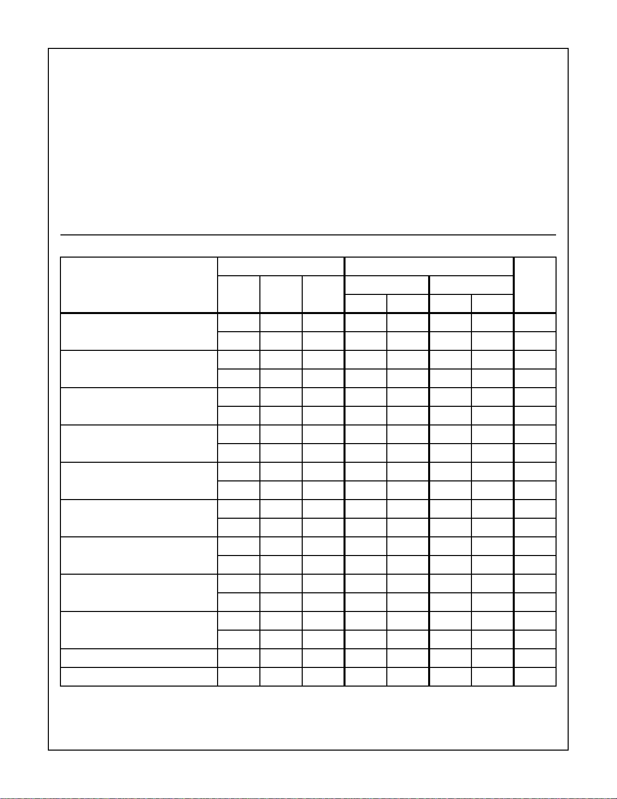
Static Electrical Specifications
CONDITIONS LIMITS
Thermal Resistance (Typical, Note 1) θJA (oC/W) θJC (oC/W)
SBDIP Package. . . . . . . . . . . . . . . . . . 55 15
Maximum Junction Temperature . . . . . . . . . . . . . . . . . . . . . . +150oC
Maximum Storage Temperature Range (T
) . . .-65oC to +150oC
STG
Maximum Lead Temperature (Soldering 10s)
At Distance 1/16 ±1/32 inch (1.59 ±0.79mm) . . . . . . . . . . +265oC
PARAMETER
Quiescent Device Current I
Output Low Drive
(Sink) Current
Output High Drive
(Source) Current
Output Voltage Low-Level
(Note 1)
Output Voltage
High Level (Note 1)
Input Low Voltage V
Input High Voltage V
-55oC, +25oC +125oC
DD
V
O
(V)
- 0, 5 5 - 500 - 1000 µA
V
(V)
IN
V
(V)
DD
MIN MAX MIN MAX
UNITS
- 0, 10 10 - 500 - 1000 µA
I
OL
0.4 0, 5 5 0.75 - 0.5 - mA
0.5 0, 10 10 1.80 - 1.2 - mA
I
OH
4.6 0, 5 5 - -0.5 - -0.35 mA
9.5 0, 10 10 - -1.0 - -0.70 mA
V
OL
- 0, 5 5 - 0.1 - 0.2 V
- 0, 10 10 - 0.1 - 0.2 V
V
OH
- 0, 5 5 4.9 - 4.9 - V
- 0, 10 10 9.9 - 9.8 - V
0.5, 4.5 - 5 - 1.5 - 1.5 V
IL
0.5, 9.5 - 10 - 3 - 3 V
0.5, 4.5 - 5 3.5 - 3.5 - V
IH
0.5, 9.5 - 10 7 - 7 - V
Input Leakage Current I
Three-State Output
Leakage Current
Input Capacitance (Note 1) C
Output Capacitance (Note 1) C
NOTE:
1. Guaranteed but not tested.
I
OUT
IN
IN
OUT
- 0, 5 5 - ±1-±5 µA
- 0, 10 10 - ±1-±5 µA
0, 5 0, 5 5 - ±1-±10 µA
0, 10 0, 10 10 - ±1-±10 µA
----10-10pF
----15-15pF
5-63
Page 3
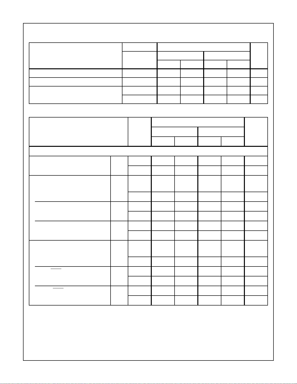
Specifications CDP1854A/3, CDP1854AC/3
Operating Conditions At T
= Full Package-Temperature Range. For maximum reliability, operating conditions should be selected so
A
that operation is always within the following ranges:
CONDITIONS LIMITS
-55oC, +25oC +125oC
V
PARAMETER
(V)
DD
MIN MAX MIN MAX
UNITS
DC Operating Voltage Range - 4 10.5 4 6.5 V
Input Voltage Range - V
SS
V
DD
V
SS
V
DD
Baud Rate (Receive or Transmit) 5 - 250 - 215 K bits/s
10 - 520 - 430 K bits/s
Dynamic Electrical Specifications t
, tF = 15ns, VIH = VDD, VIL = VSS, CL = 100pF, (See Figure 1)
R
LIMITS
-55oC, +25oC +125oC
V
PARAMETER
(V)
DD
MIN MAX MIN MAX
UNITS
TRANSMITTER TIMING - MODE 1
Clock Period t
CC
5 240 - 280 - ns
10 120 - 145 - ns
V
Pulse Width t
CL
Clock Low Level 5 105 - 125 - ns
10 55 - 65 - ns
Clock High Level t
CH
5 135 - 155 - ns
10 65 - 80 - ns
TPB t
TT
5 125 - 165 - ns
10 70 - 80 - ns
Propagation Delay Time t
CD
Clock to Data Start Bit 5 - 425 - 485 ns
10 - 205 - 235 ns
TPB to THRE t
TTH
5 - 315 - 380 ns
10 - 155 - 185 ns
Clock to THRE t
CTH
5 - 335 - 390 ns
10 - 160 - 190 ns
5-64
Page 4
CDP1854A/3, CDP1854AC/3
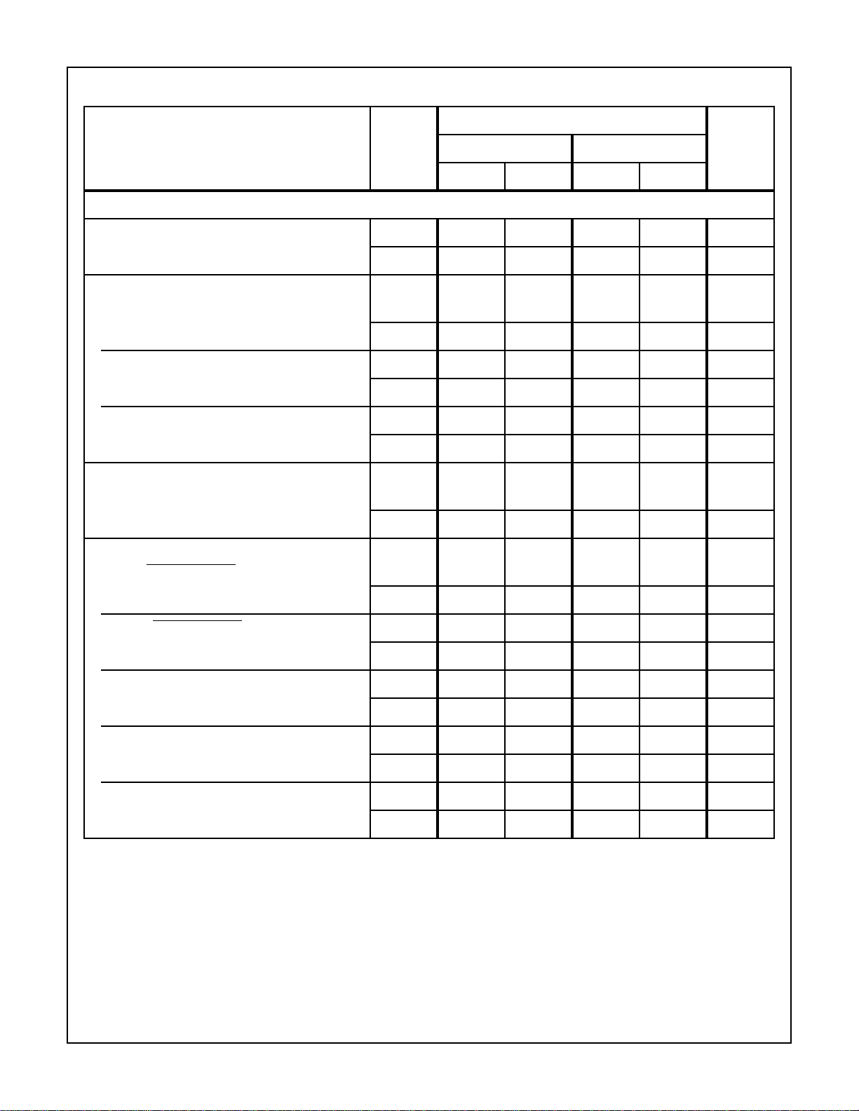
Dynamic Electrical Specifications t
PARAMETER
RECEIVER TIMING - MODE 1
Clock Period t
Pulse Width
Clock Low Level t
Clock High Level t
TPB t
Setup Time
Data Start Bit to Clock t
, tF = 15ns, VIH = VDD, VIL = VSS, CL = 100pF, (See Figure 2)
R
LIMITS
-55oC, +25oC +125oC
V
DD
CC
(V)
5 240 - 280 - ns
MIN MAX MIN MAX
10 120 - 145 - ns
CL
5 105 - 125 - ns
10 55 - 65 - ns
CH
5 135 - 155 - ns
10 65 - 80 - ns
TT
5 125 - 165 - ns
10 70 - 80 - ns
DC
5 105 - 120 - ns
UNITS
Propagation Delay Time
TPB to DATA AVAILABLE t
Clock to DATA AVAILABLE t
Clock to Overrun Error t
Clock to Parity Error t
Clock to Framing Error t
TDA
CDA
COE
CPE
CFE
10 65 - 70 - ns
5 - 295 - 340 ns
10 - 150 - 170 ns
5 - 305 - 355 ns
10 - 150 - 170 ns
5 - 305 - 330 ns
10 - 150 - 175 ns
5 - 305 - 330 ns
10 - 150 - 175 ns
5 - 280 - 330 ns
10 - 145 - 165 ns
5-65
Page 5

CDP1854A/3, CDP1854AC/3
TRANSMITTER HOLDING
REGISTER LOADED
(NOTE 1)
T CLOCK
WRITE (TPB)
(NOTE 3)
THRE
SDO
t
TT
t
TTH
TRANSMITTER SHIFT
REGISTER LOADED
(NOTE 2)
t
t
CH
12
34567141516123
t
CD
CC
t
CTH
t
CL
4
t
CD
1ST DATA BIT
NOTES:
1. The holding register is loaded on the trailing edge of TPB.
2. The transmitter shift register, if empty, is loaded on the first high-to-low transition of the clock which occurs at least 1/2 clock period + t
after the trailing edge of TPB and transmission of a start bit occurs 1/2 clock period + tCD later.
3. Write is the overlap of TPB, CS1, and CS3 = 1 and CS3, RD/WR = 0
FIGURE 1. TRANSMITTER TIMING DIAGRAM - MODE 1
TC
R CLOCK
(NOTE 1)
SDI
DA
READ
(NOTE 2)
TPB
OE
(NOTE 3)
PE
(NOTE 3)
FE
t
CC
t
CH
t
CL
12
t
DC
t
TT
CLOCK 7 1/2
SAMPLE
3456716
t
TDA
START BIT
PARITY
123456789
STOP BIT 1
CLOCK 7 1/2 LOAD
HOLDING REGISTER
t
t
CDA
COE
t
t
CPE
CFE
NOTES:
1. If a start bit occurs at a time less than tDC before a high-to-low transition of the clock, the start bit may not be recognized until the next
high-to-low transition of the clock. The start bit may be completely asynchronous with the clock.
2. Read is the overlap of CS1, CS3, RD/WR = 1 andCS2 = 0. If a pending DA has not been cleared by a read of the receiver holding register
by the time a new word is loaded into the receiver holding register, the OE signal will come true.
3. OE and PE share terminal 15 and are also available as two separate bits in the status register.
FIGURE 2. MODE 1 RECEIVER TIMING DIAGRAM
5-66
Page 6

CDP1854A/3, CDP1854AC/3
Dynamic Electrical Specifications t
PARAMETER
CPU INTERFACE - WRITE TIMING - MODE 1
Pulse Width
TPB t
Setup Time
RSEL to Write t
Data to Write t
Hold Time
RSEL after Write t
, tF = 15ns, VIH = VDD, VIL = VSS, CL = 100pF, (See Figure 3)
R
LIMITS
-55oC, +25oC +125oC
V
DD
TT
(V)
5 125 - 165 - ns
MIN MAX MIN MAX
10 70 - 80 - ns
RSW
5 20 - 10 - ns
10 25 - 25 - ns
DW
5 65 - 75 - ns
10 45 - 50 - ns
WRS
5 -10 - -20 - ns
105-5-ns
UNITS
Data after Write t
WD
5 95 - 105 - ns
10 55 - 55 - ns
TPB
(NOTE 1)
RSEL
T BUS 0-
T BUS 7
CS3, CS1
(NOTE 1)
WR, CS2
RD/
(NOTE 1)
NOTE:
1. Write is the overlap of TPB, CS1, CS3 = 1 and CS2, RD/WR = 0.
FIGURE 3. MODE 1 CPU INTERFACE (WRITE) TIMING DIAGRAM
t
RSW
t
TT
t
WRS
t
DW
t
WD
5-67
Page 7

CDP1854A/3, CDP1854AC/3
Dynamic Electrical Specifications t
PARAMETER
CPU INTERFACE - READ TIMING - MODE 1
Pulse Width
TPB t
Setup Time
RSEL to TPB t
Hold Time
RSEL after TPB t
Propagation Delay Time
Read to Data Valid Time t
, tF = 15ns, VIH = VDD, VIL = VSS, CL = 100pF, (See Figure 4)
R
LIMITS
-55oC, +25oC +125oC
V
DD
TT
(V)
5 125 - 165 - ns
MIN MAX MIN MAX
10 70 - 80 - ns
RST
515- 0 -ns
10 20 - 10 - ns
TRS
5 -10 - -25 - ns
105-0-ns
RDV
5 - 360 - 420 ns
UNITS
RESEL to Data Valid Time t
TPB
RSEL
R BUS 0-
R BUS 7
RD/WR, CS1, CS3
(NOTE 1)
CS2
RSDV
NOTE:
1. Read is the overlap of CS1, CS3, RD/WR = 1 and CS2 = 0.
FIGURE 4. MODE 1 CPU INTERFACE (READ) TIMING DIAGRAM
10 - 165 - 195 ns
5 - 250 - 295 ns
10 - 125 - 145 ns
t
TT
t
TRS
t
RDV
t
RSDV
t
RST
5-68
Page 8

CDP1854A/3, CDP1854AC/3
Dynamic Electrical Specifications t
PARAMETER
INTERFACE TIMING - MODE 0
Pulse Width
CRL t
MR t
Setup Time
Control Word to CRL t
Hold Time
Control Word after CRL t
Propagation Delay Time
SFD High to SOD t
SFD Low to SOD t
RRD High to Receiver Register
High Impedance
RRD Low to Receiver Register Active t
, tF= 15ns, VIH = VDD, VIL = VSS, CL = 100pF, (See Figure 5)
R
LIMITS
-55oC, +25oC +125oC
MIN MAX MIN MAX
CRL
V
DD
(V)
5 105 - 125 - ns
10 55 - 65 - ns
MR
5 340 - 385 - ns
10 160 - 175 - ns
CWC
5 80 - 85 - ns
10 40 - 60 - ns
CCW
5 65 - 65 - ns
10 45 - 45 - ns
SFDH
5 - 175 - 195 ns
10 - 105 - 115 ns
SFDL
5 165 - 195 - ns
10 90 - 105 - ns
t
RRDH
5 - 185 - 205 ns
10 - 110 - 130 ns
RRDL
5 165 - 195 - ns
10 90 - 105 - ns
UNITS
CONTROL WORD INPUT
CRL
STATUS OUTPUTS
SFD
R BUS 0
R BUS 7
RRD
CONTROL INPUT WORD TIMING
CONTROL WORD BYTE
t
CWC
t
CRL
STATUS OUTPUT TIMING
t
SFDH
RECEIVER REGISTER DISCONNECT TIMING
t
RRDH
FIGURE 5. MODE 0 INTERFACE TIMING DIAGRAM
5-69
t
CCW
t
RRDL
t
SFDL
Page 9

CDP1854A/3, CDP1854AC/3
Dynamic Electrical Specifications t
PARAMETER
TRANSMITTER TIMING - MODE 0
Clock Period t
Pulse Width
Clock Low Level t
Clock High Level t
THRL t
Setup Time
THRL to Clock t
Data to THRL t
Hold Time
Data after THRL t
Propagation Delay Time
Clock to Data Start Bit t
Clock to THRE t
THRL to THRE t
Clock to TSRE t
, tF = 15ns, VIH = VDD, VIL = VSS, CL = 100pF, (See Figure 6)
R
LIMITS
-55oC, +25oC +125oC
MIN MAX MIN MAX
CC
V
DD
(V)
5 240 - 280 - ns
10 120 - 145 - ns
CL
5 105 - 125 - ns
10 55 - 65 - ns
CH
5 135 - 155 - ns
10 65 - 80 - ns
THTH
5 140 - 165 - ns
10 80 - 85 - ns
THC
5 205 - 235 - ns
10 120 - 140 - ns
DT
5 25 - 30 - ns
10 20 - 25 - ns
TD
5 60 - 95 - ns
10 45 - 75 - ns
CD
5 - 435 - 505 ns
10 - 205 - 235 ns
CT
5 - 345 - 420 ns
10 - 175 - 200 ns
TTHR
5 - 275 - 325 ns
10 - 145 - 165 ns
TTS
5 - 345 - 405 ns
10 - 165 - 190 ns
UNITS
5-70
Page 10

CDP1854A/3, CDP1854AC/3
TRANSMITTER HOLDING
REGISTER LOADED
(NOTE 1)
t
CC
t
THC
t
THTH
t
TTHR
t
CL
t
DT
DAT A
T CLOCK
THRL
SDO
THRE
TSRE
T BUS 0
T BUS 7
t
CH
NOTES:
1. The holding register is loaded on the trailing edge of THRL.
2. The transmitter shift register, if empty, is loaded on the first high-to-low transition of the clock which occurs at least 1/2 clock period + t
after the trailing edge of THRL and transmission of a start bit occurs 1/2 clock period + tCD later.
FIGURE 6. MODE 0 TRANSMITTER TIMING DIAGRAM
TRANSMITTER SHIFT
REGISTER LOADED
(NOTE 2)
12
t
TTS
t
TD
34567141516123
t
CD
1ST DATA BIT
t
CT
t
CD
THC
R CLOCK
(NOTE 1)
SDI
R BUS 0 -
R BUS 7
DA
DAR
OE
(NOTE 2)
PE
FE
t
CC
t
CH
t
CL
12
t
DC
CLOCK 7 1/2
SAMPLE
3456716
START BIT
t
DDA
t
DD
PARITY
123456789
STOP BIT 1
CLOCK 7 1/2 LOAD
HOLDING REGISTER
t
COE
t
CPE
t
CFE
t
CDV
DAT A
t
CDA
NOTES:
1. If a start bit occurs at a time less than tDC before a high-to-low transition of the clock, the start bit may not be recognized until the next
high-to-low transition of the clock. The start bit may be completely asynchronous with the clock.
2. If a pending DA has not been cleared by a read of the receiver holding register by the time a new word is loaded into the receiver holding
register, the OE signal will come true.
FIGURE 7. MODE 0 RECEIVER TIMING DIAGRAM
5-71
Page 11

CDP1854A/3, CDP1854AC/3
Dynamic Electrical Specifications t
PARAMETER
RECEIVER TIMING - MODE 0
Clock Period t
Pulse Width
Clock Low Level t
Clock High Level t
DATA AVAILABLE RESET t
Setup Time
Data Start Bit to Clock t
Propagation Delay Time
DATA AVAILABLE RESET to
Data Available
Clock to Data Valid t
Clock to Data Available t
Clock to Overrun Error t
Clock to Parity Error t
Clock to Framing Error t
, tF = 15ns, VIH = VDD, VIL = VSS, CL = 100pF, (See Figure 7)
R
LIMITS
-55oC, +25oC +125oC
MIN MAX MIN MAX
CC
V
DD
(V)
5 240 - 280 - ns
10 120 - 145 - ns
CL
5 105 - 125 - ns
10 55 - 65 - ns
CH
5 135 - 155 - ns
10 65 - 80 - ns
DD
5 75 - 90 - ns
10 45 - 50 - ns
DC
5 105 - 130 - ns
10 65 - 85 - ns
t
DDA
5 - 240 - 280 ns
10 - 130 - 145 ns
CDV
5 - 360 - 420 ns
10 - 175 - 195 ns
CDA
5 - 320 - 375 ns
10 - 155 - 180 ns
COE
5 - 365 - 415 ns
10 - 170 - 190 ns
CPE
5 - 275 - 320 ns
10 - 135 - 155 ns
CFE
5 - 270 - 320 ns
10 - 135 - 165 ns
UNITS
5-72
Page 12

CDP1854A/3, CDP1854AC/3
16 / f
CLOCK
NEXT DATA WORD
START BIT
Burn-In Circuit
STOP BITS 1, 1-1/2 OR 2
DAT A
LSB
5 - 8 DATA BITS
DAT A
MSB
PARITY BIT
FIGURE 8. SERIAL DATA WORD FORMAT
V
DD
V
SS
1
2
3
4
5
6
7
8
9
10
11
12
13
14
15
16
17
18
19
20
40
39
38
37
36
35
34
33
32
31
30
29
28
27
26
25
24
23
22
21
V
DD
V
SS
ALL RESISTORS ARE 47kΩ±20%
TYPE V
DD
TEMPERATURE TIME
CDP1854A/3 11 +125oC 160 hrs.
CDP1854AC/3 7 +125oC 160 hrs.
FIGURE 9. BIAS/STATIC BURN-IN CIRCUIT
All Intersil semiconductor products are manufactured, assembled and tested under ISO9000 quality systems certification.
Intersil products are sold by description only. Intersil Corporation reserves the right to make changes in circuit design and/or specifications at any time without
notice. Accordingly, the reader is cautioned to verify that data sheets are current before placing orders. Information furnished by Intersil is believed to be accurate
and reliable. However, no responsibility is assumed by Intersil or its subsidiaries for its use; nor for any infringements of patents or other rights of third parties which
may result from its use. No license is granted by implication or otherwise under an y patent or patent rights of Intersil or its subsidiaries.
For information regarding Intersil Corporation and its products, see web site http://www.intersil.com
5-73
 Loading...