

Page 1
CDP1852,
CDP1852C
March 1997
Features
• Static Silicon-Gate CMOS Circuitry
• Parallel 8-Bit Data Register and Buffer
• Handshaking Via Service Request Flip-Flop
• Low Quiescent and Operating Power
• Interfaces Directly with CDP1800-Series
Microprocessors
• Single Voltage Supply
o
• Full Military Temperature Range (-55
C to +125oC)
Ordering Information
PACKAGE TEMP. RANGE 5V 10V
PDIP -40oC to +85oC CDP1852CE CDP1852E E24.6
SBDIP -40oC to +85oC CDP1852CD CDP1852D D24.6
PKG.
NO.
Byte-Wide Input/Output Port
Description
The CDP1852 and CDP1852C are parallel, 8-bit, mode-programmable input/output ports. They are compatible and will
interface directly with CDP1800-series microprocessors. They
are also useful as 8-bit address latches when used with the
CDP1800 multiplexed address bus and as I/O ports in generalpurpose applications.
The mode control is used to program the device as an input port
(mode = 0) or as an output port (mode = 1). The
can be used as a signal to indicate when data is ready to be
transferred. In the input mode, a peripheral device can strobe
data into the CDP1852, and microprocessor can read that data
by device selection. In the output mode, a microprocessor
strobes data into the CDP1852, and handshaking is established
with a peripheral device when the CDP1852 is deselected.
In the input mode, data at the data-in terminals (DI0-DI7) is
strobed into the port’s 8-bit register by a high (1) level on the
clock line. The negative high-to-low transition of the clock
latches the data in the register and sets the service request output low (
(CS1/
SR/SR = 0). When CS1/CS1 and CS2 are high
CS1 and CS2 = 1), the three-state output drivers are
enabled and data in the 8-bit register appear at the data-out terminals (D00-D07). When either CS1/
CS1 or CS2 = 0), the data-out terminals are three-stated
(CS1/
CS1 or CS2 goes low
and the service request output returns high (
In the output mode, the output drivers are enabled at all times.
Data at the data-in terminals (DI0-DI7) is strobed into the 8-bit
register when CS1/
CS1 is low (CS1/CS1 = 0) and CS2 and the
clock are high (1), and are present at the data-out terminals
(D00-D07). The negative high-to-low transition of the clock
latches the data in the register. The
SR/SR = 1) when the device is deselected (CS1/CS1 = 1 or
(
CS2 = 0) and returns low (
SR/SR = 0) on the following trailing
SR/SR output goes high
edge of the clock.
SR/SR output
SR/SR =1).
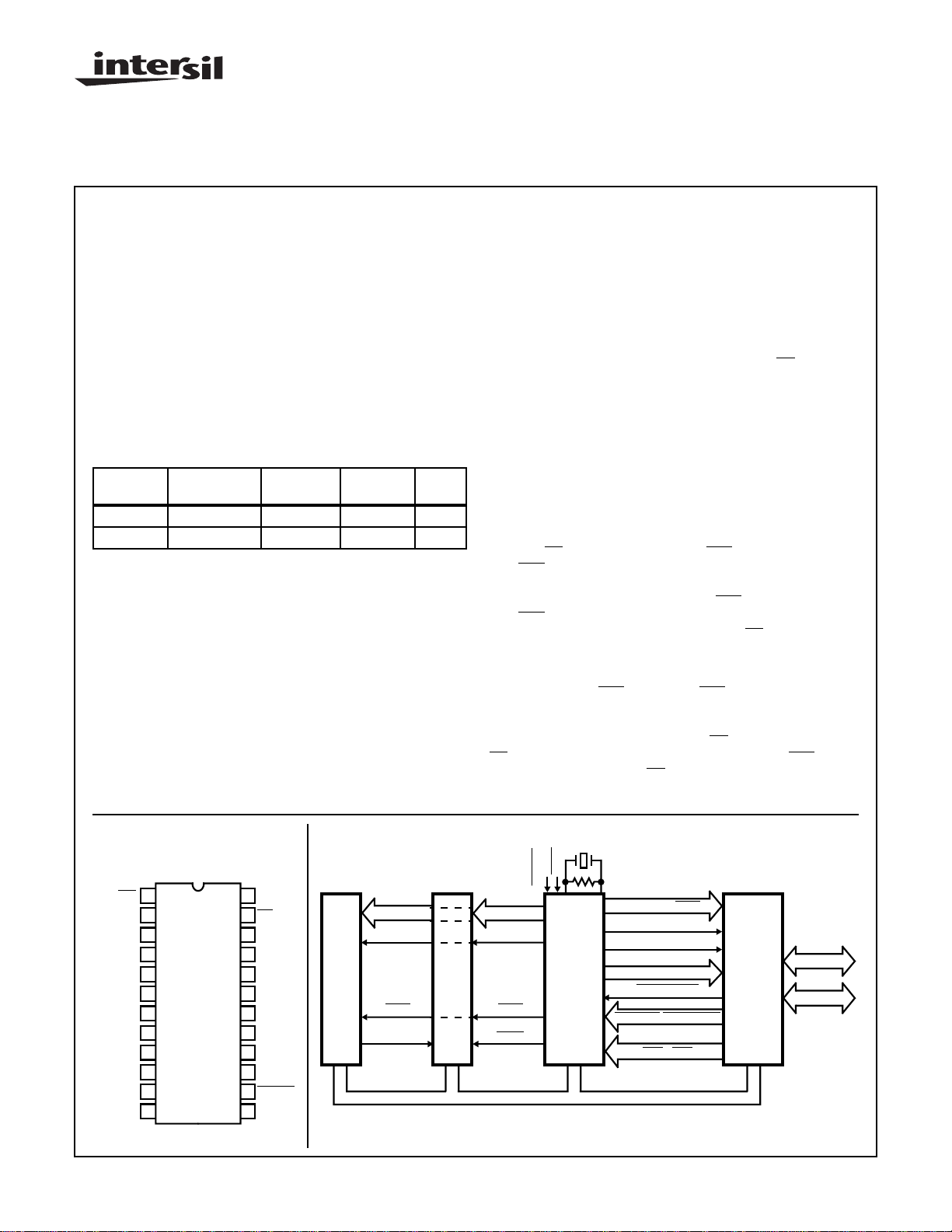
Pinout
24 LEAD DIP
TOP VIEW
1
CSI
CSI/
MODE
2
DI0
3
DO0
4
5
DI1
DO1
6
DI2
7
DO2
8
DI3
9
DO3
10
CLOCK
11
V
12
SS
CAUTION: These devices are sensitive to electrostatic discharge; follow proper IC Handling Procedures.
http://www.intersil.com or 407-727-9207
24
23
22
21
20
19
18
17
16
15
14
13
V
DD
SR/SR
DI7
DO7
DI6
DO6
DI5
DO5
DI4
DO4
CLEAR
CS2
Typical CDP1802 Microprocessor System
WAIT
CLEAR
ADDR BUS
TPA
MRD
CEO
| Copyright © Intersil Corporation 1999
ADDR BUS
TPA
RAMROM
MRD
MWR
BIDIRECTIONAL DATA BUS
4-19
CPU
CDP1802
FIGURE 1.
N0 - N2
MRD
TPB
Q
SC0 SC1
INTERRUPT
DMA - IN DMA - OUT
EF1 - EF4
I/O
CDP1852
File Number
DAT A
CONTROL
1166.2
Page 2
CDP1852, CDP1852C
Absolute Maximum Ratings Thermal Information
DC Supply-voltage Range, (VDD)
(Voltage Referenced to VSSTerminal)
CDP1852 . . . . . . . . . . . . . . . . . . . . . . . . . . . . . . . . . .-0.5 to +11V
CDP1852C . . . . . . . . . . . . . . . . . . . . . . . . . . . . . . . . . .-0.5 to +7V
Input Voltage Range, All Inputs . . . . . . . . . . . . . . -0.5 to VDD +0.5V
DC Input Current, Any One Input. . . . . . . . . . . . . . . . . . . . . . . . .±10mA
Device Dissipation Per Output Transistor . . . . . . . . . . . . . . . 100mW
For TA = Full Package-Temperature Range
(All Package Type)
CAUTION: Stresses above those listed in “Absolute Maximum Ratings” may cause permanent damage to the device. This is a stress only rating and operation
of the device at these or any other conditions above those indicated in the operational sections of this specification is not implied.
Thermal Resistance (Typical) θJA (oC/W) θJC (oC/W)
PDIP Package. . . . . . . . . . . . . . . . . . . 65 N/A
SBDIP Package. . . . . . . . . . . . . . . . . . 65 20
Operating-Temperature Range (TA)
Package Type D, H . . . . . . . . . . . . . . . . . . . . . . .-55oC to +125oC
Package Type E. . . . . . . . . . . . . . . . . . . . . . . . . . .-40oC to +85oC
Storage Temperature Range (T
) . . . . . . . . . . . .-65oC to +150oC
STG
Lead Temperature (During Soldering): . . . . . . . . . . . . . . . . . +265oC
At Distance 1/16 ± 1/32 inch (1.59 ± 0.79mm)
from Case for 10s max
Operating Conditions At T
= Full Package Temperature Range. For Maximum Reliability, Operating Conditions Should be
A
Selected so that Operation is Always within the Following Ranges:
LIMITS
CDP1852 CDP1852C
PARAMETER
MIN MAX MIN MAX
DC Operating Voltage Range 4 10.5 4 6.5 V
Input Voltage Range V
SS
V
DD
V
SS
V
DD
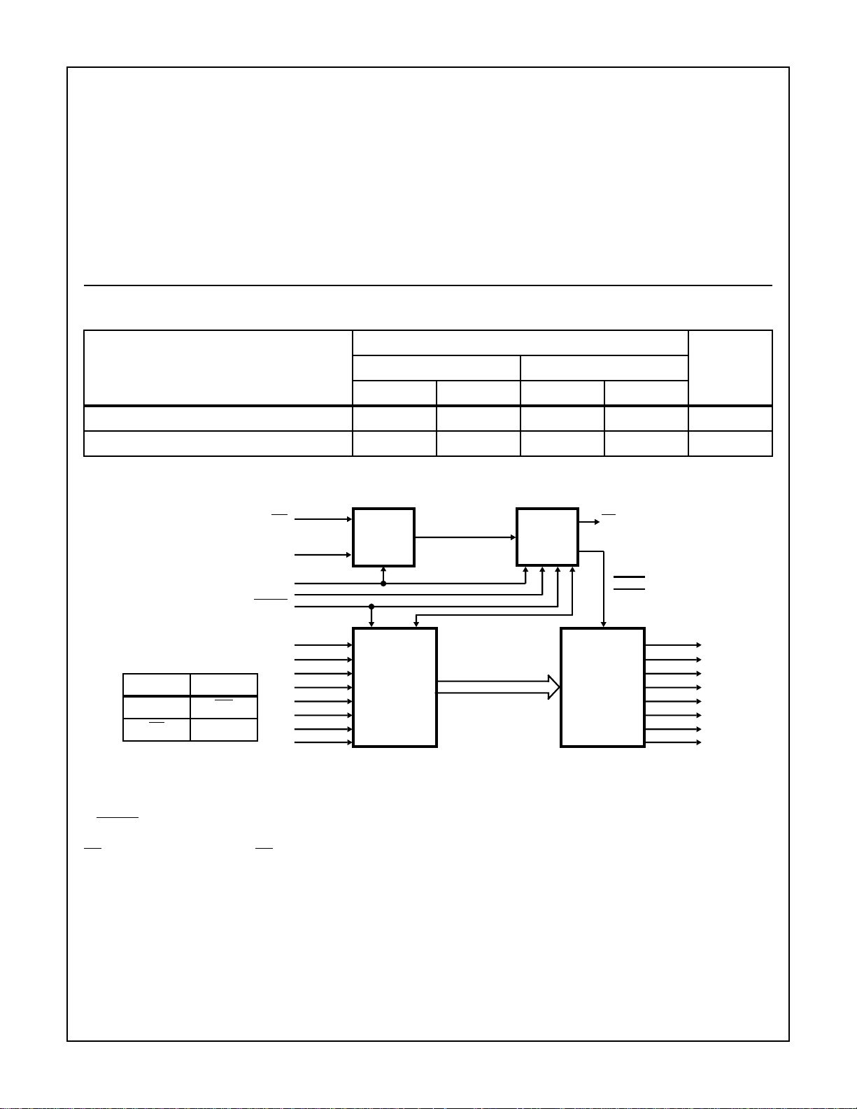
Functional Diagram
MODE 0 MODE 1
P1 CSI CSI
P23 SR SR
CSI/
CSI
(NOTE 1)
CS2
MODE
CLOCK
CLEAR
DI0
DI1
DI2
DI3
DI4
DI5
DI6
DI7
13
11
14
16
18
20
22
1
2
3
5
7
9
DEVICE
SELECT
DECODE
RESET
8-BIT
DAT A
REGISTER
CONTROL
LOGIC
CLOCK
23
SR/SR
(NOTE 1)
24
12
ENABLE
THREE-
STATE
OUTPUT
DRIVERS
V
DD
V
SS
4
DO0
6
DO1
8
DO2
10
DO3
15
DO4
17
DO5
19
DO6
21
DO7
UNITS
V
NOTE:
1. Polarity depends on mode.
FIGURE 2. FUNCTIONAL BLOCK DIAGRAM FOR CDP1852
A CLEAR control is provided for resetting the port’s register
(DO0-DO7 = 0) and service request flip-flop (input mode:
SR/ SR = 1 and output mode: SR/SR = 0).
The CDP1852 is functionally identical to the CDP1852C.
The CDP1852 has a recommended operating voltage range
of 4 to 10.5 volts, and the CDP1852C has a recommended
operating voltage range of 4 to 6.5 volts.
The CDP1852 and CDP1852C are supplied in 24-lead,
hermetic, dual-in-line ceramic packages (D suffix), in 24-lead
dual-in-line plastic packages (E suffix). The CDP1852C is
also available in chip form (H suffix).
4-20
Page 3
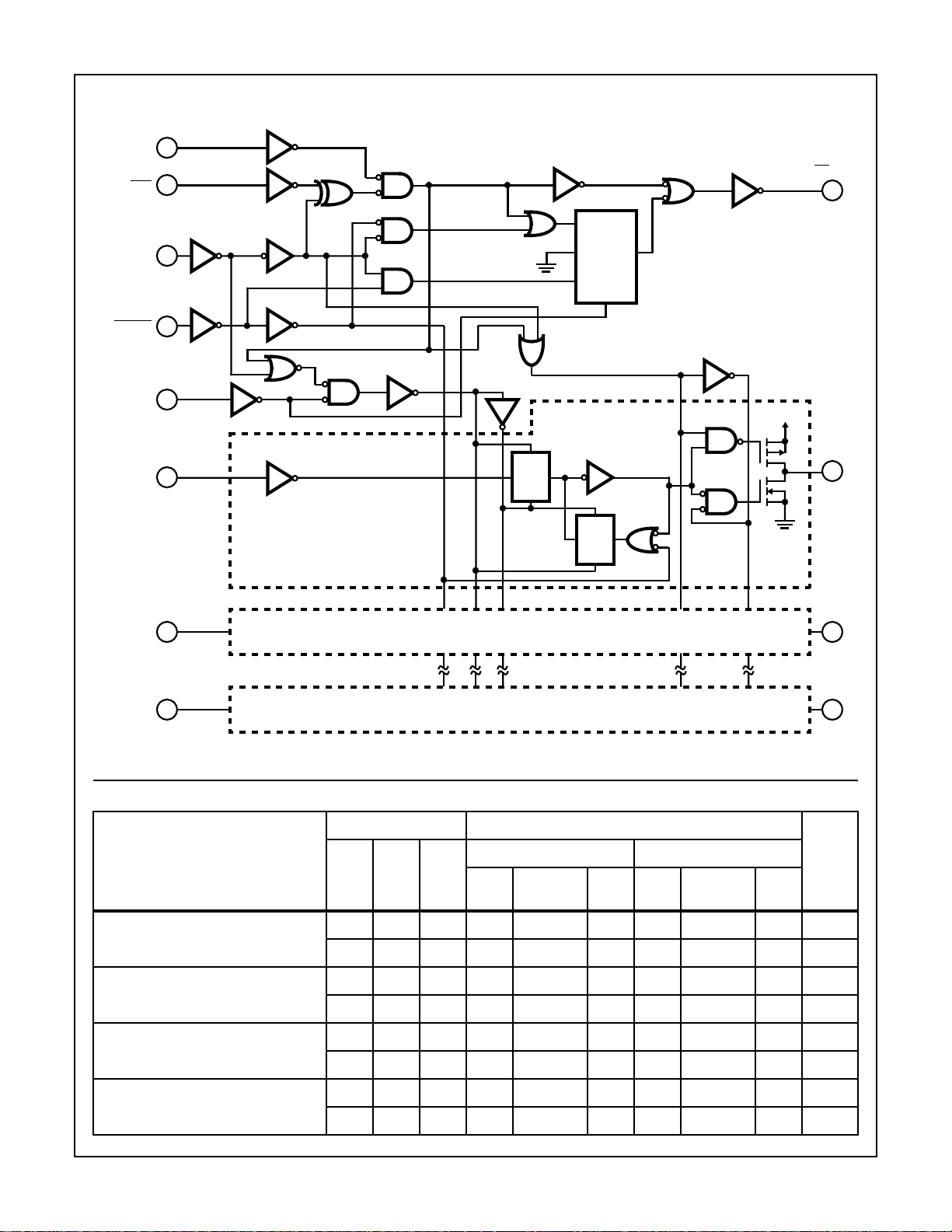
Logic Diagram
13
CS2
MODE
1
2
14
CS1/CS1
CLEAR
CDP1852, CDP1852C
V
SS
SR/SR
23
S
D
Q
R
CL
SERVICE
REQUEST
LATCH
DI0
DI1
DI7
11
3
5
22
CLOCK
Static Electrical Specifications At T
p
TG
n
p
TG
n
FIGURE 3. CDP1852 LOGIC DIAGRAM
= -40oC to +85oC, Unless Otherwise Specified
A
CONDITIONS LIMITS
V
DD
p
DO0
4
n
V
SS
DO1
6
DO7
21
PARAMETER
Quiescent Device Current I
Output Low Drive
(Sink) Current
Output High Drive
(Source) Current
Output Voltage Low-Level
(Note 2)
CDP1852 CDP1852C
V
V
DD
(V)
V
IN
DD
(V)
MIN
O
(V)
- 0, 5 5 - - 10 - - 50 µA
(NOTE1)
TYP MAX MIN
(NOTE1)
TYP MAX
UNITS
- 0, 10 10 - - 100 - - - µA
I
0.4 0, 5 5 1.6 3.2 - 1.6 3.2 - mA
OL
0.5 0, 10 10 3 6 - - - - mA
I
4.6 0, 5 5 -1.15 -2.3 - -1.15 -2.3 - mA
OH
9.5 0, 10 10 -3 -6 - - - - mA
V
OL
- 0, 5 5 - 0 0.1 - 0 0.1 V
- 0, 10 10 - 0 0.1 - - - V
4-21
Page 4

CDP1852, CDP1852C
Static Electrical Specifications At T
PARAMETER
Output Voltage High Level
(Note 2)
Input Low Voltage V
Input High Voltage V
Input Leakage Current I
Three-State Output Leakage
Current
V
OH
IL
lH
lN
I
OUT
0, 10 0, 10 10 - - ±2---µA
= -40oC to +85oC, Unless Otherwise Specified (Continued)
A
CONDITIONS LIMITS
CDP1852 CDP1852C
V
V
(V)
(V)
V
IN
DD
(V)
MIN
O
(NOTE1)
TYP MAX MIN
(NOTE1)
TYP MAX
UNITS
- 0, 5 5 4.9 5 - 4.9 5 - V
- 0, 10 10 9.9 10 - - - - V
0.5,
- 5 - - 1.5 - - 1.5 V
4.5
0.5,
-10--3---V
9.5
0.5,
- 5 3.5 - - 3.5 - - V
4.5
0.5,
-107-----V
9.5
- 0, 5 5 - - ±1- - ±1 µA
- 0, 10 10 - - ±2---µA
0, 5 0, 5 5 - - ±1- - ±1 µA
Operating Current (Note 3) I
DD1
- 0, 5 5 - 130 300 - 150 300 µA
- 0, 10 10 - 550 800 - - - µA
Input Capacitance C
Output Capacitance C
OUT
- - - - 5 7.5 - 5 7.5 pF
IN
- - - - 5 7.5 - - - pF
NOTES:
1. Typical values are for TA = 25oC and nominal VDD.
2. IOL = IOH = 1µA
3. Operating current is measured at 2MHz in an CDP1802 system with open outputs and a program of 6N55, 6NAA, 6N55, 6NAA,....
Dynamic Electrical Specifications At T
= -40oC to +85oC, VDD = ±5%, tR, tF = 20ns, VIH = 0.7 VDD, VIL = 0.3 VDD, CL = 100pF,
A
and 1 TTL Load
LIMITS
PARAMETER
V
DD
(V)
(NOTE 1)
TYP MAX
UNITSMIN
MODE 0 - INPUT PORT (See Figure 4)
Minimum Select Pulse Width t
SW
5 - 180 360 ns
10 - 90 180 ns
Minimum Write Pulse Width t
WW
5 - 90 180 ns
10 - 45 90 ns
Minimum Clear Pulse Width t
CLR
5 - 80 160 ns
10 - 40 80 ns
4-22
Page 5

CDP1852, CDP1852C
Dynamic Electrical Specifications At T
PARAMETER
Minimum Data Setup Time t
Minimum Data Hold Time t
Data Out Hold Time (Note 2) t
Propagation Delay Times, t
Select to Data Out (Note 2) t
Clear to SR t
Clock to SR t
PLH
, t
PHL
= -40oC to +85oC, VDD = ±5%, tR, tF = 20ns, VIH = 0.7 VDD, VIL = 0.3 VDD, CL = 100pF,
A
and 1 TTL Load (Continued)
DS
DH
DOH
SDO
RSR
CSR
LIMITS
V
DD
(V)
5 - -10 0 ns
10 - -5 0 ns
5 - 75 150 ns
10 - 35 75 ns
5 30 185 370 ns
10 15 100 200 ns
5 30 185 370 ns
10 15 100 200 ns
5 - 170 340 ns
10 - 85 170 ns
5 - 110 220 ns
10 - 55 110 ns
(NOTE 1)
TYP MAX
UNITSMIN
Select to SR t
NOTES:
1. Typical values are for TA = 25oC and nominal VDD.
2. Minimum value is measured from CS2, maximum value is measured from CS1/CS1.
SSR
5 - 120 240 ns
10 - 60 120 ns
Input Port Mode 0 - Typical Operation
General Operation
When the mode control is tied to V
, the CDP1852
SS
becomes an input port. In this mode, the peripheral device
places data into the CDP1852 with a strobe pulse and the
CDP1852 signals the microprocessor that data is ready to
be transferred on the strobe’s trailing edge via the
SR output
line. The CDP1802 then issues an input instruction that
enables the CDP1852 to place the information from the
peripheral device on the data bus to be entered into a memory location and the accumulator of the microprocessor.
Detailed Operation (See Figure 5)
The STROBE from the peripheral device places DATA into
the 8-bit register of the CDP1852 when it goes high and
latches the DATA on its trailing edge. The
SR output is set
low on the strobe’s trailing edge. This output is connected to
a flag line of the CDP1802 microprocessor and software
polling will determine that the flag line has gone low and
peripheral data is ready to be transferred. The CDP1802
then issues an input instruction that places an N
With the
MRD line also high, the CDP1852 is selected and
line high.
X
its output drivers place the DATA from the per ipheral device
on the DATA BUS. When the CDP1802 selected the
CDP1852, it also selected and addressed the memory via
one of the 16 internal address registers selected by an
internal “X” register. The data from the CDP1852 is theref ore
entered into the memory [Bus → M(R(X))]. The data is also
transferred to the D register (accumulator) in the
microprocessor (Bus → D). When the CDP1802’s execute
cycle is completed, the CDP1852 is deselected by the N
line returning low and its data output pins are three-stated.
The
SR output returns high.
X
4-23
Page 6

CDP1852, CDP1852C
CS1 - CS2
(NOTE 1)
CLOCK
DATA IN
DATA BUS
SR
t
RSR
CLEAR
t
CLR
NOTE 1. CS1 • CS2 is the overlap of CS1 = 1 and CS2 = 1.
t
WW
t
DS
MODE 0 TRUTH TABLE
CLOCK † CS1-CS2 CLEAR DATA OUT EQUALS
X 0 X High Impedance
0100
0 1 1 Data Latch
1 1 X Data In
† CS1 • CS2: CS1 = 1, CS2 = 1
t
DH
HIGH
IMPEDANCE
t
CSR
t
SW
t
t
DOH
SSR
t
SDO
SERVICE REQUEST TRUTH TABLE
CLOCK CS1 or CS2
or CLEAR
SR/SR 0 SR/SR 1
STROBE
PERIPHERAL
DAT A
SR/SR
N
MRD
FIGURE 4. MODE 0 INPUT PORT TIMING WAVEFORMS AND TRUTH TABLES
VALID THREE - STATEDATA BUS
CS2
CS1
SR
MODE
CDP1852
CLOCK
D0
D1
STROBE
DATA FROM
PERIPHERAL
PERIPHERAL DEVICE
PLACES DATA IN CDP1852
AND CDP1852 SIGNALS
CDP1802 THAT DATA IS READY
CDP1802 SELECTS
CDP1852 AND DATA
IS TRANSFERRED
TO MEMORY AND
THE MICROPROCESSOR
MEMORY
ADDRESS
LINES
X
CDP1802
DATA BUS
N
MRD
EF
X
X
V
SS
FIGURE 5. INPUT PORT MODE 0 FUNCTIONAL DIAGRAM AND WAVEFORMS - TYPICAL OPERATION
4-24
Page 7

CDP1852, CDP1852C
Dynamic Electrical Specifications At T
PARAMETER
MODE 1- OUTPUT PORT (See Figure 6)
Minimum Clock Pulse Width t
Minimum Write Pulse Width t
Minimum Clear Pulse Width t
Minimum Data Setup Time t
Minimum Data Hold Time t
Minimum Select-After-Clock Hold Time t
Propagation Delay Times, t
Clear to Data Out t
Write to Data Out t
Data In to Data Out t
Clear to SR t
Clock to SR t
Select to SR t
NOTE:
1. Typical values are for TA = 25oC and nominal VDD.
PLH
, t
PHL
= -40oC to +85oC, VDD=±5%, tR, tF = 20ns, VIH = 0.7 VDD, VIL = 0.3 VDD, CL = 100pF,
A
and 1 TTL Load
CLK
WW
CLR
DS
DH
SH
RDO
WDO
DDO
RSR
CSR
SSR
LIMITS
V
DD
(V)
5 - 130 260 ns
10 - 65 130 ns
5 - 130 260 ns
10 - 65 130 ns
5 - 60 120 ns
10 - 30 60 ns
5 - -10 0 ns
10 - -5 0 ns
5 - 75 150 ns
10 - 35 75 ns
5 - -10 0 ns
10 - -5 0 ns
5 - 140 280 ns
10 - 70 140 ns
5 - 220 440 ns
10 - 110 220 ns
5 - 100 200 ns
10 - 50 100 ns
5 - 120 240 ns
10 - 60 120 ns
5 - 120 240 ns
10 - 60 120 ns
5 - 120 240 ns
10 - 60 120 ns
(NOTE 1)
TYP MAX
UNITSMIN
Output Port Mode 1 - Typical Operation
General Operation
Connecting the mode control to V
CDP1852 as an output port. The output drivers are always
on in this mode, so any data in the 8-bit register will be
present at the data-out lines when the CDP1852 is selected.
The N line and
MRD connections between the CDP1852
and CDP1802 remain the same as in the input mode
configuration, but now the clock input of the CDP1852 is tied
to the TPB output of the CDP1802 and the SR output of the
CDP1852 will be used to signal the peripheral device that
valid data is present on its input lines. The microprocessor
issues an output instruction, and data from the memory is
strobed into the CDP1852 with the TPB pulse. When the
CDP1852 is deselected, the SR output goes high to signal
the peripheral device.
configures the
DD
Detailed Operation (See Figure 7)
The CDP1802 issues an output instruction. The N
high and the
MRD line goes low. The memory is accessed
line goes
X
M(R(X)) → BUS and places data on the DATA BUS. This
data are strobed into the 8-bit register of the CDP1852 when
TPB goes high and latched on the TPB’s trailing edge. The
valid data thus appears on the CDP1852 output lines. When
the CDP1802 output instruction cycle is complete, the N
line goes low and the SR output goes high. SR will remain
high until the trailing edge of the next TPB pulse, when it will
return low.
4-25
X
Page 8

CS1 ⋅ CS2
(NOTE 1)
CLOCK
DATA IN
t
DATA OUT
SR
CLEAR
NOTES
1. CS1 • CS2 is the overlap of CS1 = 0 and CS2 = 1.
2. Write is the overlap of CS1 • CS2 and CLOCK.
RDO
t
RSR
t
CLR
MODE 1 TRUTH TABLE
CLOCK †
CS1-CS2 CLEAR DATA OUT EQUALS
0X00
0 X 1 Data Latch
X 0 1 Data Latch
1 1 X Data In
CS1 • CS2 : CS1 = 0, CS2 = 1
†
FIGURE 6. MODE 1 OUTPUT PORT TIMING WAVEFORMS AND TRUTH TABLES
CDP1852, CDP1852C
t
(NOTE 2)
WW
t
SH
t
DH
t
DS
t
DDO
t
WDO
t
SSR
CS1
or
CS2
t
CLK
SERVICE REQUEST TRUTH TABLE
CLOCK
or
CLEAR
SR/SR 1 SR/SR 0
t
CSR
N
TPB
MRD
DATA BUS
DATA TO
PERIPHERAL
DEVICE
SR/SR
MEMORY
ADDRESS
LINES
X
CDP1802
DATA BUS
VALID
N
MRD
TPB
DATA
CDP1852
X
CS2
CS1
CLOCK
V
MODE
DD
DAT A
OUT
DATA IN
SR
DATA OUT TO
PERIPHERAL DEVICE
SIGNAL THAT INDICATES
DATA IS READY
CDP1852 IS SELECTED
AND DATA IS
STROBED INTO IT’S
REGISTER WITH TPB
DATA IS OUTPUTTED
FROM THE CDP1852
AND THE PERIPHERAL
DEVICE IS SIGNALED
FIGURE 7. OUTPUT PORT MODE 1 FUNCTIONAL DIAGRAM AND WAVEFORMS - TYPICAL OPERATION
4-26
Page 9

Application Information
CDP1852, CDP1852C
In a CDP1800 series microprocessor-based system where
MRD is used to distinguish between INP and OUT
instructions, an lNP instruction is assumed to occur at the
beginning of every I/O cycle because
MRD starts high.
Therefore, at the start of an OUT instruction, which uses the
same 3-bit N code as that used for selection of an input port,
This condition forces SR low and sets the internal SR latch
(see Figure 3). In a small system with unique N codes for
inputs and outputs, this situation does not arise. Using the
CDP1853 N-bit decoder or equivalent logic to decode the N
lines after TPA prevents dual selection in larger systems
(see Figure 9 and Figure 10).
the input device is selected for a short time (see Figure 8).
MRD
N0
N1
N2
SELECT
SR
FIGURE 8. EXECUTION OF A “65” OUTPUT INSTRUCTION SHOWING MOMENTARY SELECTION OF INPUT PORT “D”
6D 65
4
OUT 0
5
OUT 1
6
OUT 2
7
OUT 3
12
OUT 4
11
OUT 5
10
OUT 6
9
OUT 7
TPA
TPB
CE
EN
(NOTE 1)
OUTPUT
FIGURE 9. CDP1853 TIMING WAVEFORMS
2
N0
1 OF 8
DECODER
EN
Qn
CE
CLOCK A
(TPA)
CLOCK B
(TPB)
N1
N2
3
14
13
1
15
FIGURE10. CDP1853 FUNCTIONAL DIAGRAM
NOTE:
1. Output enabled when EN = HIGH. Internal signal shown for reference only (See Figure 1).
All Intersil semiconductor products are manufactured, assembled and tested under ISO9000 quality systems certification.
Intersil products are sold by description only. Intersil Corporation reserves the right to make changes in circuit design and/or specifications at any time without
notice. Accordingly, the reader is cautioned to verify that data sheets are current before placing orders. Information furnished by Intersil is believed to be accurate
and reliable. However, no responsibility is assumed by Intersil or its subsidiaries f or its use; nor for any infringements of patents or other rights of third parties which
may result from its use. No license is granted by implication or otherwise under an y patent or patent rights of Intersil or its subsidiaries.
For information regarding Intersil Corporation and its products, see web site http://www.intersil.com
4-27
 Loading...