

Page 1
March 1997
CDP1824/3,
CDP1824C/3
High-Reliability CMOS 32-Word x 8-Bit
Static Random-Access Memory
Features
• Access Time
- 610ns. . . . . . . . . . . . . . . . . . . . . . . . . . . . . at V
- 320ns. . . . . . . . . . . . . . . . . . . . . . . . . . . . at V
• No Precharge or Clock Required
Ordering Information
PACK-
5V 10V
CDP1824CD3 CDP1824D3 SBDIP -55oC to
Pinout
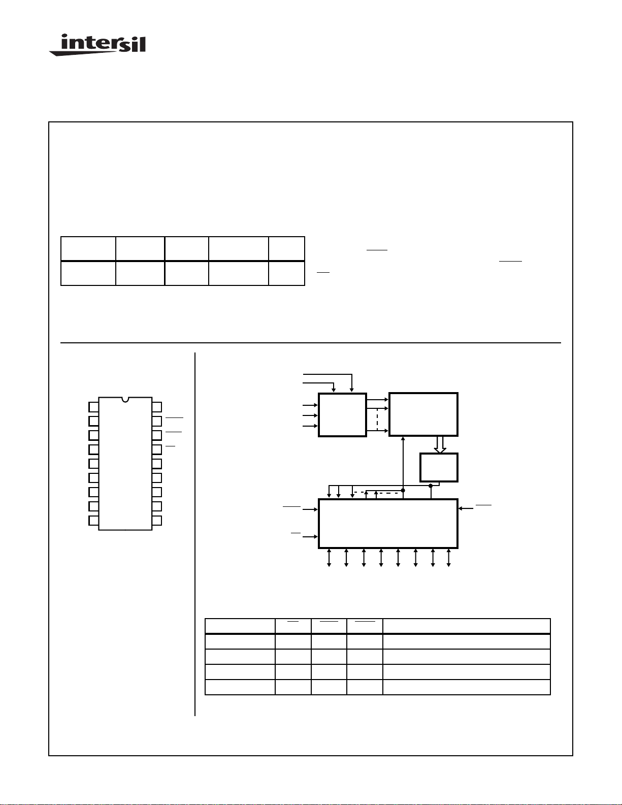
CDP1824/3, CDP1824C/3 (SBDIP)
TOP VIEW
1
MA4
2
MA3
3
MA2
4
MA1
5
MA0
6
BUS7
7
BUS6
8
BUS5
9
V
SS
AGE TEMP. RANGE
Functional Diagram
18
V
DD
17
MWR
16
MRD
15
CS
14
BUS0
13
BUS1
12
BUS2
BUS3
11
10
BUS4
+125oC
DD
DD
D18.3
V
V
= 5V
= 10V
PKG.
NO.
MA4
MA3
MA2
MA1
MA0
MWR
= 18
DD
= 9
SS
Description
The CDP1824/3 and CDP1824C/3 types are high-reliability
CMOS 32-word x 8-bit fully static random-access memories
for use in CDP1800-series microprocessor systems. These
parts are compatible with the CDP1802 microprocessor and
will interface directly without additional components.
The CDP1824/3 is fully decoded and does not require a precharge or clocking signal for proper operation. It has common input and output and is operated from a single voltage
supply. The
three-state output drivers, and overrides the
CS input is provided for memory expansion.
The CDP1824C/3 is functionally identical to the CDP1824/3.
The CDP1824/3 has a recommended operating voltage
range of 4V to 10.5V, and the CDP1824C/3 has an operating
voltage range of 4V to 6.5V.
21
3
ADDRESS
4
DECODER
5
17
I/O BUFFERS
15
CS
6 7 8 10 11 12 13 14
BUS7BUS6BUS5BUS4BUS3BUS2BUS1BUS
MRD signal (output disable control) enables the
MWR signal. A
32 X 8-BIT
ARRAY
SENSE
AMPL
16
MRD
0
OPERATIONAL MODES
FUNCTION CS MRD MWR DATA PINS STATUS
READ 0 0 X Output: High/Low Dependent on Data
WRITE 0 1 0 Input: Output Disabled
Not Selected 1 X X Output Disabled: High-Impedance State
Standby 0 1 1 Output Disabled: High-Impedance State
Logic 1 = High Logic 0 = Low X = Don’t Care
CAUTION: These devices are sensitive to electrostatic discharge; follow proper IC Handling Procedures.
http://www.intersil.com or 407-727-9207
| Copyright © Intersil Corporation 1999
6-42
File Number 1717.2
Page 2
CDP1824/3, CDP1824C/3
Absolute Maximum Ratings Thermal Information
DC Supply Voltage Range, (VDD)
(All Voltages Referenced to VSS Terminal)
CDP1824/3 . . . . . . . . . . . . . . . . . . . . . . . . . . . . . . . -0.5V to +11V
CDP1824C/3. . . . . . . . . . . . . . . . . . . . . . . . . . . . . . . . .-0.5 to +7V
Input Voltage Range, All Inputs . . . . . . . . . . . . . -0.5V to VDD +0.5V
DC Input Current, Any One Input. . . . . . . . . . . . . . . . . . . . . . . . .±10mA
Thermal Resistance (Typical, Note 1) θJA (oC/W) θJC (oC/W)
SBDIP Package. . . . . . . . . . . . . . . . . . 75 20
Device Dissipation Per Output Transistor
TA = Full Package Temperature Range
(All Package Types). . . . . . . . . . . . . . . . . . . . . . . . . . . . . . 100mW
Operating Temperature Range (TA)
Package Type D. . . . . . . . . . . . . . . . . . . . . . . . . .-55oC to +125oC
Storage Temperature Range (T
Lead Temperature (During Soldering)
At distance 1/16 ±1/32 In. (1.59 ± 0.79mm)
from case for 10s max. . . . . . . . . . . . . . . . . . . . . . . . . . . . +265oC
). . . . . . . . . . . .-65oC to +150oC
STG
Recommended Operating Conditions T
= Full Package-Temperature Range. For maximum reliability, nominal operating con-
A
ditions should be selected so that operation is always within the following ranges:
LIMITS
CDP1824/3 CDP1824C/3
PARAMETER
MIN MAX MIN MAX
UNITS
DC Operating Voltage Range 4 10.5 4 6.5 V
Input Voltage Range V
SS
V
DD
V
SS
V
DD
V
Static Electrical Specifications
CONDITIONS LIMITS
-55oC, +25oC +125oC
MIN MAX MIN MAX
UNITS
PARAMETER SYMBOL
Quiescent Device Current
(Note 1)
Output Voltage Low-Level
(Note 2)
Output Voltage High-Level
(Note 2)
Input Low Voltage V
V
O
(V)
I
DD
- 0, 5 5 - 50 - 500 µA
- 0, 10 10 - 500 - 1000 µA
V
OL
- 0, 5 5 - 0.1 - 0.2 V
- 10 - 0.1 - 0.2 V
V
OH
- 0, 5 5 4.9 - 4.8 - V
- - 10 9.9 - 4.8 - V
IL
0.5, 4.5 - 5 - 1.5 - 1.5 V
V
(V)
IN
V
DD
(V)
1, 9 - 10 - 3 - - V
Input High Voltage V
IH
0.5, 4.5 - 5 3.5 - 3.5 - V
1, 9 - 10 7 - 7 - V
Output Low Drive (Sink)
Current
Output High Drive (Source)
Current
Input Current I
Three-State Output
Leakage Current
Input Capacitance C
Output Capacitance C
I
OL
I
OH
I
OUT
OUT
0.4 0, 5 5 4 - 1.5 - mA
0.5 0, 10 10 4 - 2.9 - mA
4.6 0, 5 5 - -1 - -0.75 mA
9.5 0, 10 10 - -2 - -1.5 mA
IN
Any
Input
0, 55-1-5µA
0, 10 10 - 1 - 5 µA
0, 5 0, 5 5 - 2 - 5 µA
0, 10 0, 10 10 - 2 - 5 µA
IN
(Note 2) - 10 - 10 pF
(Note 2) - 15 - 15 pF
NOTES:
1. The CDP1824C/3 meets all 5V Static Electrical Characteristics of the CDP1824/3 except Quiescent Device Current for which the limits
are IDD = 200µA at +25oC/-55oC; IDD = 1000µA at +125oC.
2. Guaranteed, but not tested.
6-43
Page 3

CDP1824/3, CDP1824C/3
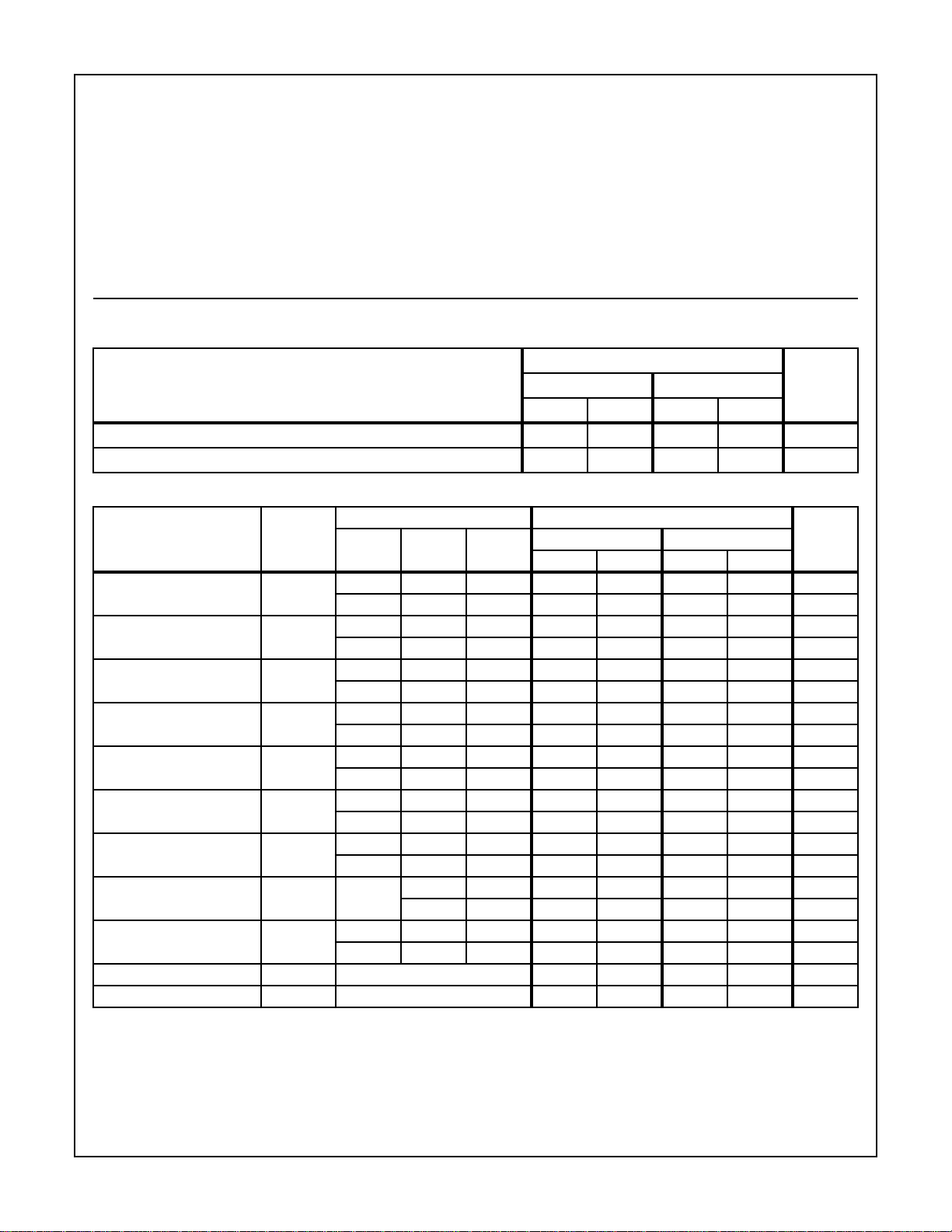
Read Cycle Dynamic Electrical Specifications Input t
TEST
CONDITIONS
V
PARAMETER SYMBOL
Access Time From Address Change t
Access Time From Chip Select t
Output Active From MRD t
MRD
MA
AA
DOA
AM
DD
(V) MIN MAX MIN MAX
5 - 610 - 825 ns
10 - 320 - 375 ns
5 - 610 - 825 ns
10 - 320 - 375 ns
5 - 610 - 825 ns
10 - 320 - 375 ns
t
AM
(NOTE 1)
, tF≤ 15ns, CL = 50pF
R
-55oC, +25oC +125oC
t
AA
LIMITS
UNITS
CS
t
DOA
DATA OUT
HIGH IMPEDANCE
(NOTE 1)
NOTE:
1. Minimum timing for valid data output longer times will initiate an earlier, but invalid output.
FIGURE 1. READ CYCLE TIMING DIAGRAM
6-44
Page 4

CDP1824/3, CDP1824C/3
Write Cycle Dynamic Electrical Specifications Input t
TEST
CONDITIONS
V
PARAMETER SYMBOL
Write Pulse Width t
Data Setup Time t
Data Hold Time t
Chip Select Setup Time t
Address Setup Time t
WRW
DS
DH
CS
AS
NOTE:
1. Time required by a device to allow for the indicated function.
DD
(V)
5 350 - 475 - ns
10 180 - 220 - ns
5 400 - 560 - ns
10 190 - 260 - ns
5 70 - 90 - ns
10 35 - 45 - ns
5 550 - 775 - ns
10 340 - 475 - ns
5 550 - 775 - ns
10 340 - 475 - ns
, tF≤ 15ns, CL = 50pF
R
-55oC, +25oC +125oC
(NOTE 1)
MIN MAX
LIMITS
(NOTE 1)
MIN MAX
UNITS
MA
t
AS
CS
t
CS
t
MWR
BUS
WRW
t
DS
t
DH
FIGURE 2. WRITE CYCLE TIMING DIAGRAM
All Intersil semiconductor products are manufactured, assembled and tested under ISO9000 quality systems certification.
Intersil products are sold by description only. Intersil Corporation reserves the right to make changes in circuit design and/or specifications at any time without
notice. Accordingly, the reader is cautioned to verify that data sheets are current before placing orders. Information furnished by Intersil is believed to be accurate
and reliable. However, no responsibility is assumed by Intersil or its subsidiaries for its use; nor for any infringements of patents or other rights of third parties which
may result from its use. No license is granted by implication or otherwise under an y patent or patent rights of Intersil or its subsidiaries.
For information regarding Intersil Corporation and its products, see web site http://www.intersil.com
6-45
Page 5

CDP1824/3, CDP1824C/3
Data Retention Specifications At T
PARAMETER SYMBOL
Data Retention Voltage V
Data Retention Quiescent Current I
Chip Deselect to Data Retention Time t
Recovery to Normal Operation Time t
V
DD
t
CDR
= +25oC
A
DR
DD
CDR
RC
TEST
LIMITS
CONDITIONS
V
DR
(V)
V
DD
(V) MIN MAX MIN MAX
CDP1824/3 CDP1824C/3
- - 2.5 - 2.5 - V
2.5 - - 10 - 40 µA
2.5 5 600 - 600 - ns
2.5 10 300 - - - ns
2.5 5 600 - 600 - ns
2.5 10 300 - - - ns
DATA RETENTION
MODE
0.95 V
DD
V
DD
t
F
(NOTE 1) (NOTE 1)
0.95 V
t
F
DD
t
RC
UNITS
CS
NOTE: tr, tf > 1µs.
FIGURE 3. LOW VDD DATA RETENTION WAVEFORMS AND TIMING DIAGRAM
Static Burn-In Circuit
V
IH
V
IL
V
DD V
V
SS
TYPE V
1
2
3
4
5
6
7
8
9
18
17
16
15
14
13
12
11
10
All Resistors 47kΩ (±20%)
DD
TEMPERATURE TIME
V
SS
CDP1824 11V +125oC 160 Hrs., Min.
DD
V
IH
V
IL
CDP1824C 7V +125oC 160 Hrs., Min.
6-46
 Loading...