

Page 1
March 1997
CDP1823C/3
High-Reliability CMOS
128-Word x 8-Bit Static RAM
Features
• For Applications in Aerospace, Military, and Critical
Industrial Equipment
• Compatible with CDP1800-Series Microprocessors at
Maximum Speed
• Interfaces with CDP1800-Series Microprocessors
without Additional Components
• Fast Access Time
• At V
= 5V, +25oC . . . . . . . . . . . . . . . . . . . . . . . .275ns
DD
• Single Voltage Supply
• Common Data Inputs and Outputs
• Multiple Chip Select Inputs to Simplify Memory
System Expansion
• High Noise Immunity. . . . . . . . . . . . . . . . . . 30% of V
• Memory Retention for Standby Battery Voltage Down
to 2V at 25
o
C
DD
• Latch-Up-Free Transient Radiation Tolerance
Ordering Information
PART NUMBER
PACKAGE TEMP. RANGE
SBDIP -55oC to +125oC CDP1823CD3 D24.6
(5V) PKG. NO.
Description
The CDP1823C/3 is a 128 word x 8-bit CMOS/SOS static
random access memory. It is compatible with the CDP1802,
CDP1804, CDP1805, and CDP1806 microprocessors, and
will interface directly without additional components. The
CDP1823C has a recommended operating voltage range of
4V to 6.5V.
The CDP1823C memory has 8 common data input and data
output terminals for direct connection to a bidirectional data
bus and is operated from a single voltage supply. Five chip
select inputs are provided to simplify memory system
expansion. In order to enable the CDP1823C , the chip select
inputs
CS2, CS3, and CS5 require a low input signal, and
the chip select inputs CS1 and CS4 require a high input
signal.
The
MRD signal enables all 8 output drivers when in the low
state and should be in a high state during a write cycle.
After valid data appear at the output, the address inputs may
be changed immediately. Output data will be valid until either
the
MRD signal goes high, the device is deselected, or t
(access time) after address changes.
AA
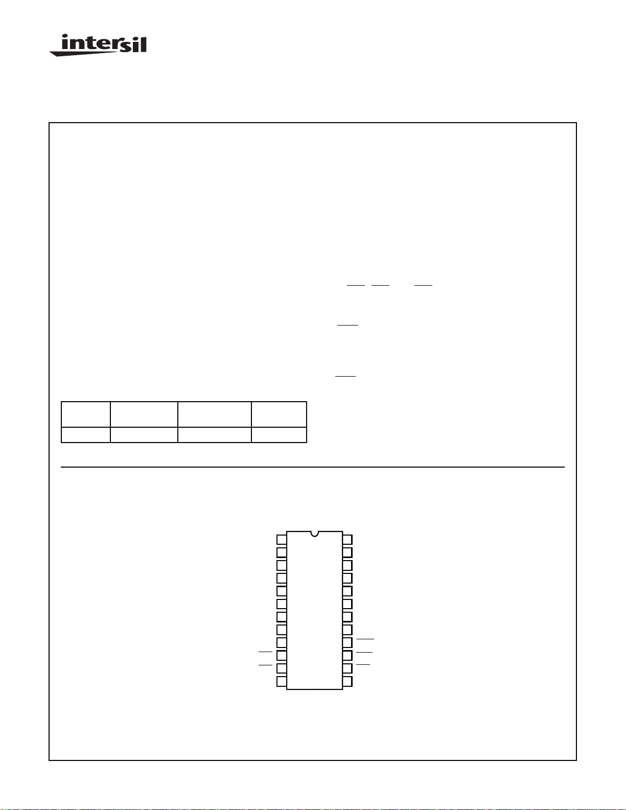
Pinout
CDP1823C/3
(SBDIP)
TOP VIEW
1
BUS 0
2
BUS 1
BUS 2
3
4
BUS 3
5
BUS 4
6
BUS 5
7
BUS 6
BUS 7
8
CS1
9
10
CS2
11
CS3
V
12
SS
CAUTION: These devices are sensitive to electrostatic discharge; follow proper IC Handling Procedures.
http://www.intersil.com or 407-727-9207
| Copyright © Intersil Corporation 1999
6-31
24
V
DD
A0
23
22
A1
A2
21
A3
20
A4
19
A5
18
A6
17
16
MWR
15
MRD
14
CS5
13
CS4
File Number 2982.1
Page 2
CDP1823C/3
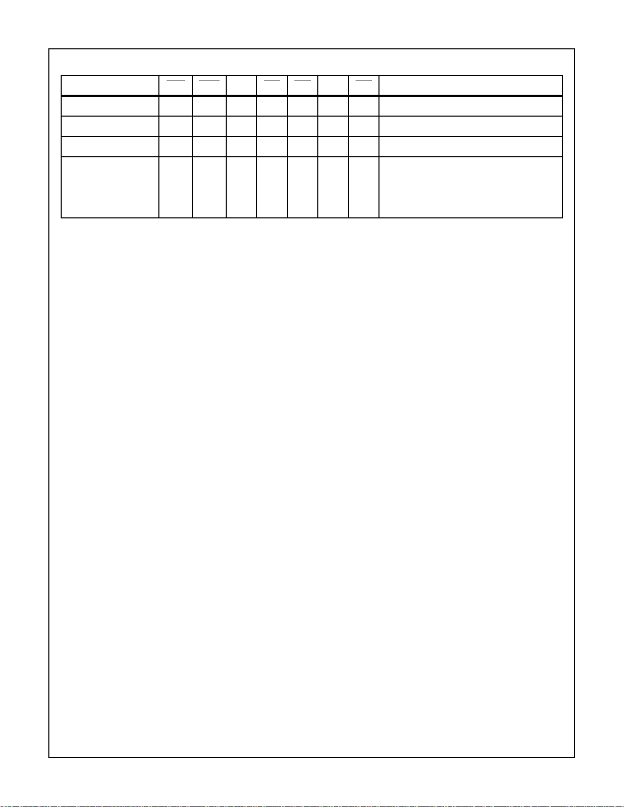
OPERATIONAL MODES
FUNCTION MRD MWR CS1 CS2 CS3 CS4 CS5 BUS TERMINAL STATE
Read 0 X 10010Storage State of Addressed Word
Write 1 0 10010Input High Impedance
Standby 1 1 10010High Impedance
Not Selected X
X
X
X
X
NOTE:
1. Logic 1 = High, Logic 0 = Low, X = Don’t Care.
X
X
X
X
X
0
X
X
X
X
High Impedance
X
1
X
X
X
X
X
1
X
X
X
X
X
0
X
X
X
X
X
1
6-32
Page 3

CDP1823C/3
Absolute Maximum Ratings
DC Supply Voltage Range, (VDD)
(All Voltages Referenced to VSS Terminal)
CDP1823C/3 . . . . . . . . . . . . . . . . . . . . . . . . . . . . . . -0.5V to +7V
Input Voltage Range, All Inputs . . . . . . . . . . . . .-0.5V to VDD +0.5V
DC Input Current, Any One Input. . . . . . . . . . . . . . . . . . . . . . . . .±10mA
Thermal Information
Thermal Resistance (Typical) θJA (oC/W) θJC (oC/W)
SBDIP Package. . . . . . . . . . . . . . . . . . 60 17
Maximum Operating Temperature Range (TA) . . . .-55oC to +125oC
Maximum Storage Temperature Range (T
Maximum Lead Temperature (During Soldering) . . . . . . . . .+265oC
) . . .-65oC to +150oC
STG
Maximum Junction Temperature. . . . . . . . . . . . . . . . . . . . . . +150oC
Recommended Operating Conditions At T
= Full Package Temperature Range. For maximum reliability, operating
A
conditions should be selected so that operation is always within the following ranges:
LIMITS
PARAMETER
UNITSMIN MAX
Supply Voltage Range 4 6.5 V
Recommended Input Voltage Range V
Static Electrical Specifications V
= 5V ±5%
DD
SS
V
DD
V
CONDITIONS LIMITS
-55oC, +25oC +125oC
PARAMETER
Quiescent Device Current (Note 1) I
Output Low (Sink) Current (Note 1) I
Output High (Source) Current (Note 1) I
Output Voltage Low-Level V
Output Voltage High-Level V
Input Low Voltage V
Input High Voltage V
Input Leakage Current (Note 1) I
Operating Current (Note 1) I
Three-State Output Leakage Current I
Input Capacitance C
Output Capacitance C
DD
OL
OH
OL
OH
IL
IH
IN
DD1
OUT
IN
OUT
V
O
(V)
- 0, 5 5 - 270 - 1000 µA
0.4 0, 5 5 2.7 - 1.5 - mA
4.6 0, 5 5 - -1.3 - -0.7 mA
- 0, 5 5 - 0.1 - 0.1 V
- 0, 5 5 VDD - 0.1 - VDD - 0.1 - V
0.5, 4.5 - 5 - 0.3 V
0.5, 4.5 - 5 0.7 V
- 0, 5 5 - ±2.6 - ±10 µA
- 0, 5 5 - 5 - 10 mA
0, 5 0, 5 5 - ±2.6 - ±10 µA
- - - - 7.5 - 7.5 pF
----15-15pF
V
(V)
V
IN
(V)
DD
MIN MAX MIN MAX
- 0.3 V
DD
-V
DD
DD
- 0.7 V
DD
UNITS
V
NOTE:
1. Limits designate 100% testing, all other limits are designer’s parameters under given test conditions and do not represent 100% testing.
Read Cycle Dynamic Electrical Specifications t
PARAMETER SYMBOL
Read Cycle t
Access Time from Address Change (Note 1) t
Access Time from Chip Select t
RC
AA
AC
, tF = 10ns, CL = 50pF
R
LIMITS
+25oC, -55oC +125oC
V
DD
(V)
MIN MAX MIN MAX
5 360 - 505 - ns
5 - 360 - 505 ns
5 - 360 - 505 ns
6-33
UNITS
Page 4

CDP1823C/3
Read Cycle Dynamic Electrical Specifications t
, tF = 10ns, CL = 50pF (Continued)
R
LIMITS
+25oC, -55oC +125oC
V
PARAMETER SYMBOL
Access Time from MRD (Note 1) t
Data Hold Time After Read t
AM
DH
DD
(V)
MIN MAX MIN MAX
UNITS
5 - 310 - 435 ns
5 50 - 70 - ns
NOTE:
1. Limits designate 100% testing. All other limits are designer’s parameters under given test conditions and do not represent 100% testing.
t
RC
t
AA
ADDRESS
t
AM
MRD
(NOTE 1)
CS2, CS3, CS5
(NOTE 1)
t
AC
CS1, CS4
HIGH IMPEDANCE
VALID DATA
NOTES:
1. Minimum timing for valid data output. Longer times will initiate an earlier but invalid output.
2. MWR is high during read operation. Timing measurement reference is 0.5VDD.
FIGURE 1. READ CYCLE TIMING DIAGRAM
Write Cycle Dynamic Electrical Specifications t
, tF= 10ns, CL = 50pF
R
+25oC, -55oC +125oC
PARAMETER SYMBOL
Write Cycle t
WC
V
DD
(V)
5 280 - 400 - ns
(NOTE 2)
MIN MAX
LIMITS
(NOTE 2)
t
DH
90%
10%
MIN MAX
UNITS
Address Setup Time (Note 1) t
Address Hold Time t
Write Pulse Width (Note 1) t
Data to MWR Setup Time (Note 1) t
AS
AH
WW
DS
5 70 - 100 - ns
5 70 - 100 - ns
5 140 - 200 - ns
5 70 - 100 - ns
6-34
Page 5

CDP1823C/3
Write Cycle Dynamic Electrical Specifications t
, tF= 10ns, CL = 50pF (Continued)
R
LIMITS
+25oC, -55oC +125oC
PARAMETER SYMBOL
Data Hold Time from MWR (Note 1) t
Chip Select Setup t
DH
CS
V
DD
(V)
5 50 - 70 - ns
5 210 - 300 - ns
(NOTE 2)
MIN MAX
(NOTE 2)
MIN MAX
UNITS
NOTES:
1. Limits designate 100% testing. All other limits are designer’s parameters under given test conditions and do not represent 100% testing.
2. Minimum timing to allow the indicated function to occur.
t
WC
t
AH
t
CS
ADDRESS
CS1, CS4
CS2, CS3, CS5
t
AS
t
MWR
BUS 0-7
WW
t
DS
VALID DATA
t
DH
NOTE:
1. MRD must be high during write operation.
FIGURE 2. WRITE CYCLE TIMING WAVEFORMS
Data Retention Specifications
TEST
CONDITIONS LIMITS
+25oC, -55oC +125oC
MIN MAX MIN MAX
UNITS
PARAMETER SYMBOL
Minimum Data Retention Voltage
V
DR
(V)
V
DR
- - - 2 - 2.5 V
V
DD
(V)
(Note 1)
Data Retention Quiescent Current I
Chip Deselect to Data Retention Time t
Recovery to Normal Operation Time t
DD
CDR
RC
2 - - 100 - 400 µA
- 5 450 - 650 - ns
- 5 450 - 650 - ns
NOTE:
1. Limits designate 100% testing. All other limits are designer’s parameters under given test conditions and do not represent 100% testing.
6-35
Page 6

CDP1823C/3
DATA RETENTION
V
DD
0.95 V
DD
t
CDR
CS
V
IH
V
IL
FIGURE 3. LOW VDD DATA RETENTION WAVEFORMS
MODE
0.95 V
V
DR
t
f
t
r
DD
t
RC
V
IH
V
IL
R
A15
R
A14
R
A13
R = 10kΩ ±20%
A12
A11
A10
1
2
3
4
5
6
7
8
9
10
11
12
24
23
22
21
20
19
18
17
16
15
14
13
PACKAGE TEMPERATURE DURATION V
D 125oC 160 Hrs 7V
0 1.6 2.2 5.0 6.6 7.2 10.0
01
V
A0
A1
A2
A3
A4
A5
A6
01
A7
A8
A9
DD
DD
V
DD
0
V
DD
A0
0
V
DD
0A1
NOTE:
1. A1 - A11 are division by 2 based on A0.
FIGURE 4. DYNAMIC/OPERATING BURN-IN CIRCUIT AND TIMING DIAGRAM
All Intersil semiconductor products are manufactured, assembled and tested under ISO9000 quality systems certification.
Intersil products are sold by description only. Intersil Corporation reserves the right to make changes in circuit design and/or specifications at any time without
notice. Accordingly, the reader is cautioned to verify that data sheets are current before placing orders. Information furnished by Intersil is believed to be accurate
and reliable. However, no responsibility is assumed by Intersil or its subsidiaries for its use; nor for any infringements of patents or other rights of third parties which
may result from its use. No license is granted by implication or otherwise under an y patent or patent rights of Intersil or its subsidiaries.
For information regarding Intersil Corporation and its products, see web site http://www.intersil.com
6-36
 Loading...