

Page 1
March 1997
CDP1823,
CDP1823C
128-Word x 8-Bit
LSI Static RAM
Features
• Fast Access Time
= 5V . . . . . . . . . . . . . . . . . . . . . . . . . . . . . . . 450ns
-V
DD
-V
= 10V . . . . . . . . . . . . . . . . . . . . . . . . . . . . . . 250ns
DD
• Common Data Inputs and Outputs
• Multiple Chip Select Inputs to Simplify Memory
System Expansion
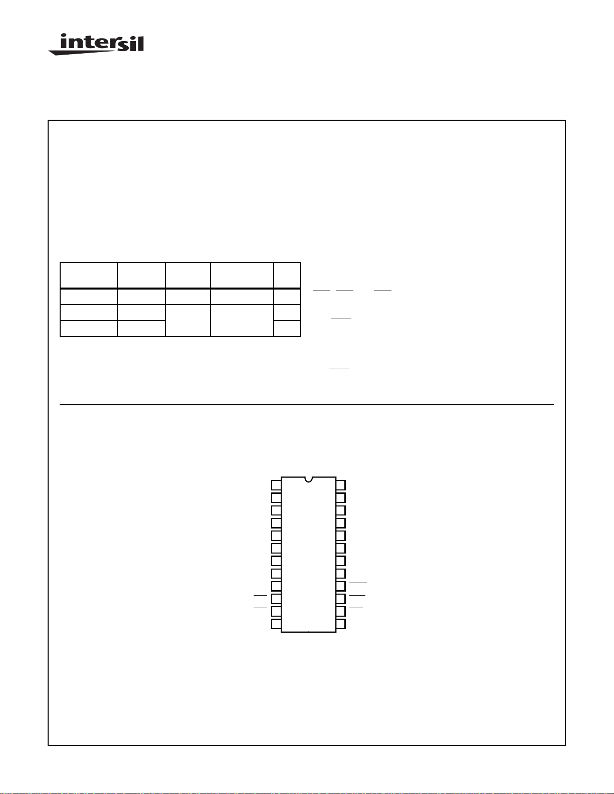
Ordering Information
PKG.
5V 10V P ACKAGE TEMP. RANGE
CDP1823CE CDP1823E PDIP -40oC to +85oC E24.6
CDP1823CD CDP1823D SBDIP -40oC to +85oC D24.6
CDP1823CDX - Burn-In D24.6
NO.
Pinout
CDP1823, CDP1823C
(PDIP, SBDIP)
Description
The CDP1823 and CDP1823C are 128-word by 8-bit CMOS
SOS static random-access memories. These memories are
compatible with general-purpose microprocessors. The two
memories are functionally identical. They differ in that the
CDP1823 has a recommended operating voltage range of
4V to 10.5V, and the CDP1823C has a recommended operating voltage range of 4V to 6.5V.
The CDP1823 memory has 8 common data input and data
output terminals for direct connection to a bidirectional data
bus and is operated from a single voltage supply. Five chipselect inputs are provided to simplify memory-system expansion. In order to enable the CDP1823, the chip-select inputs
CS2, CS3 and CS5 require a low input signal, and the chipselect inputs CS1 and CS4 require a high input signal.
The
MRD signal enables all 8 output drivers when in the low
state and should be in a high state during a write cycle.
After valid data appear at the output, the address inputs may
be changed immediately. Output data will be valid until either
the
MRD signal goes high, the device is deselected, or t
(access time) after address changes.
TOP VIEW
AA
1
BUS 0
2
BUS 1
BUS 2
3
BUS 3
4
5
BUS 4
6
BUS 5
BUS 6
7
BUS 7
8
CS1
9
10
CS2
11
CS3
12
V
SS
CAUTION: These devices are sensitive to electrostatic discharge; follow proper IC Handling Procedures.
http://www.intersil.com or 407-727-9207
| Copyright © Intersil Corporation 1999
6-24
24
V
DD
MA0
23
22
MA1
MA2
21
MA3
20
MA4
19
MA5
18
MA6
17
16
MWR
15
MRD
14
CS5
CS4
13
File Number 1198.2
Page 2
CDP1823, CDP1823C
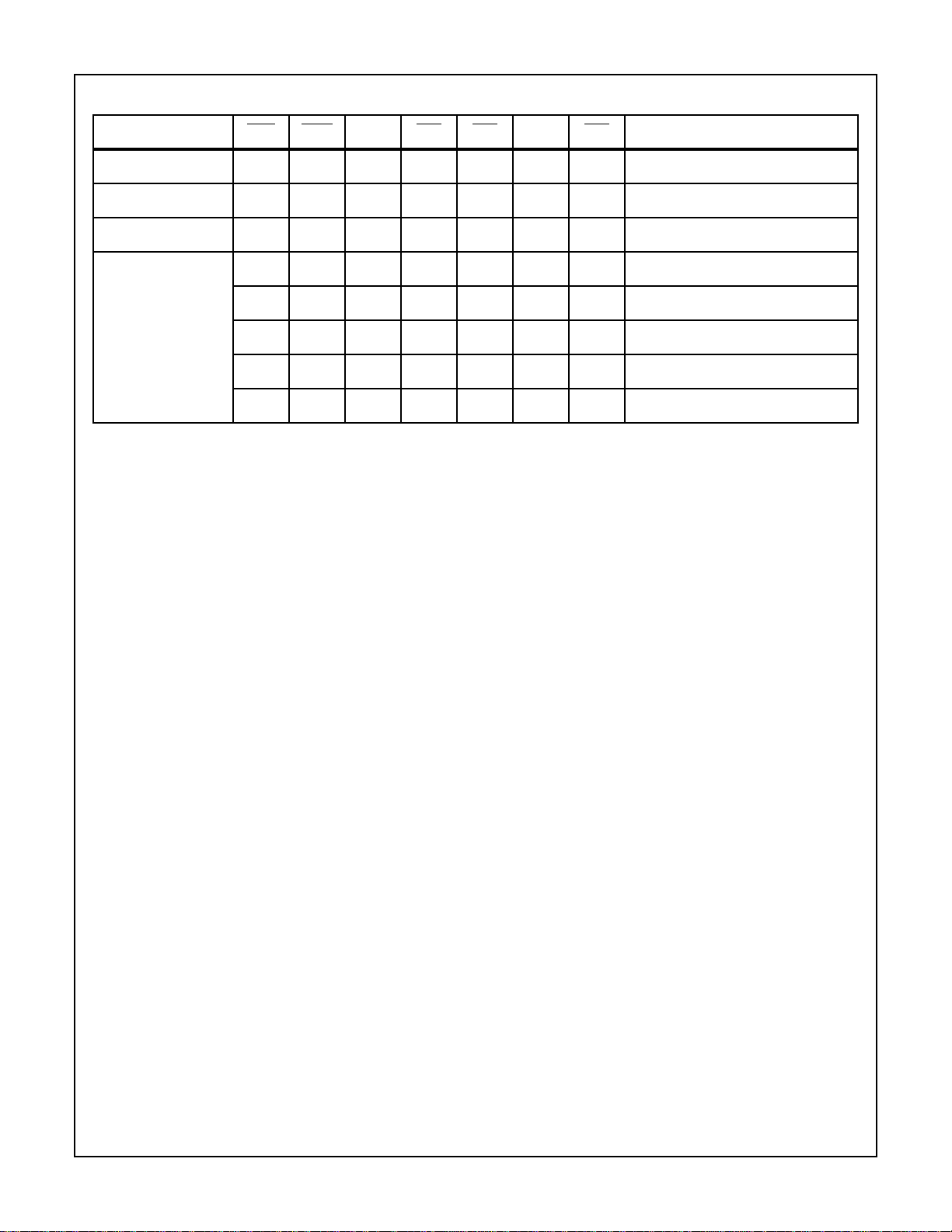
OPERATIONAL MODES
FUNCTION MRD MWR CS1 CS2 CS3 CS4 CS5 BUS TERMINAL STATE
Read 0 X 10010Storage State of Addressed Word
Write 1010010Input High-Impedance
Stand-By (Active) 1110010High Impedance
Not Selected X X 0 XXXXHigh Impedance
X X X 1 X X X High Impedance
XXXX1XXHigh Impedance
XXXXX0XHigh Impedance
XXXXXX1High Impedance
Logic 1 = High, Logic 0 = Low, X = Don’t Care
6-25
Page 3
CDP1823, CDP1823C
Absolute Maximum Ratings Thermal Information
DC Supply Voltage Range, (VDD)
(All Voltages Referenced to VSS Terminal)
CDP1823 . . . . . . . . . . . . . . . . . . . . . . . . . . . . . . . . -0.5V to +11V
CDP1823C. . . . . . . . . . . . . . . . . . . . . . . . . . . . . . . . -0.5V to +7V
Input Voltage Range, All Inputs . . . . . . . . . . . . .-0.5V to VDD +0.5V
DC Input Current, Any One Input. . . . . . . . . . . . . . . . . . . . . . . . .±10mA
Operating Temperature Range (TA)
Package Type D . . . . . . . . . . . . . . . . . . . . . . . . .-55oC to +125oC
Package Type E . . . . . . . . . . . . . . . . . . . . . . . . . . -40oC to +85oC
Thermal Resistance (Typical) θJA (oC/W) θJC (oC/W)
PDIP Package. . . . . . . . . . . . . . . . . . . 60 N/A
SBDIP Package. . . . . . . . . . . . . . . . . . 60 17
Maximum Storage Temperature Range (T
Maximum Junction Temperature
Plastic Package. . . . . . . . . . . . . . . . . . . . . . . . . . . . . . . . . +150oC
Maximum Lead Temperature (During Soldering) . . . . . . . . . . 300oC
) . . .-65oC to +150oC
STG
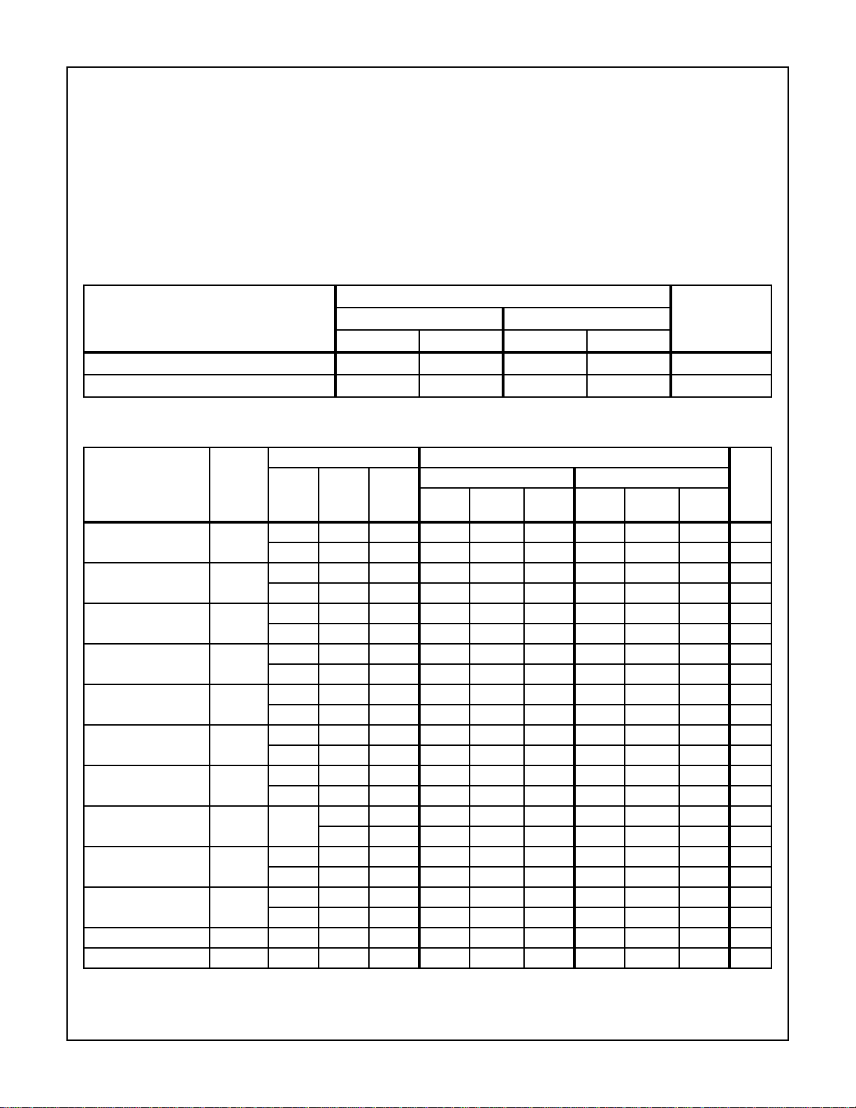
Recommended Operating Conditions At T
= Full Package Temperature Range. For maximum reliability, operating conditions
A
should be selected so that operation is always within the following ranges:
LIMITS
CDP1823D CDP1823CD
PARAMETER
MIN MAX MIN MAX
UNITS
Supply Voltage Range 4 10.5 4 6.5 V
Recommended Input Voltage Range V
Static Electrical Specifications At T
= -40oC to +85oC, Except as Noted:
A
SS
V
DD
V
SS
V
DD
CONDITIONS LIMITS
CDP1823 CDP1823C
PARAMETER SYMBOL
Quiescent Device
Current
Output Low (Sink)
Current
Output High (Source)
Current
Output Voltage
Low-Level
Output Voltage
High-Level
Input Low Voltage V
V
O
(V)
I
DD
- 0, 5 5 - - 500 - - 500 µA
- 0, 10 10 - - 1000 - - - µA
I
OL
0.4 0, 5 5 2 4 - 2 4 - mA
0.5 0, 10 10 4.5 9 - - - - mA
I
OH
4.6 0, 5 5 -1 -2 - -1 -2 - mA
9.5 0, 10 10 -2.2 -4.4 - - - - mA
V
OL
- 0, 5 5 - 0 0.1 - 0 0.1 V
- 0, 10 10 - 0 0.1 - - - V
V
OH
- 0, 5 5 4.9 5 - 4.9 5 - V
- 0, 10 10 9.9 10 - - - - V
0.5, 4.5 - 5 - - 1.5 - - 1.5 V
IL
V
(V)
V
IN
DD
(V)
MIN
(NOTE 1)
TYP MAX MIN
(NOTE 1)
TYP MAX
0.5, 9.5 - 10 - - 3 - - - V
Input High Voltage V
0.5, 9.5 - 5 3.5 - - 3.5 - - V
IH
0.5, 9.5 - 10 7 - - - - - V
Input Leakage Current I
Operating Current
(Note 2)
Three-State Output
Leakage Current
Input Capacitance C
Output Capacitance C
I
DD1
I
OUT
OUT
IN
IN
Any
Input
0, 5 5 - - ±5- - ±5 µA
0, 10 10 - - ±10 - - - µA
- 0, 5 5 - 4 8 - 4 8 mA
- 0, 10 10 - 8 16 - - - mA
0, 5 0, 5 5 - - ±5- -± 5 µA
0, 10 0, 10 10 - - ±10 - - - µA
----57.5-57.5pF
----1015-1015pF
NOTES:
1. Typical values are for TA = +25oC and nominal VDD.
2. Outputs open circuited; Cycle time = 1µs.
V
UNITS
6-26
Page 4

CDP1823, CDP1823C
Dynamic Electrical Specifications At T
PARAMETER SYMBOL
= -40 to +85oC, VDD ±5%, tR, tF = 20ns, CL = 100pF
A
V
(V)
DD
(NOTE 2)
MIN
Read Cycle (See Figure 1)
Access Time From Address
t
AA
5 - 275 450 - 275 450 ns
Change
10 - 150 250 - - - ns
Access Time From Chip
t
DOA
5 - 150 250 - 150 250 ns
Select
10 - 100 150 - - - ns
MRD to Output Active t
AM
5 - 150 250 - 150 250 ns
10 - 100 150 - - - ns
Data Hold Time After Read t
DOH
5 255075255075ns
10 15 25 40 - - - ns
NOTES:
1. Typical values are at TA = 25oC and nominal voltage.
2. Time required by a limit device to allow for the indicated function.
+
t
AA
LIMITS
CDP1823 CDP1823C
(NOTE 1)
TYP MAX
(NOTE 2)
MIN
(NOTE 1)
TYP MAX
UNITS
ADDRESS
t
AM
MRD
CS2, CS3, CS5
t
DOA
CS1, CS4
DATA OUT
HIGH IMPEDANCE
NOTE:
1. MWR is high during read operation. Timing measurement reference is 0.5 VDD.
FIGURE 1. READ CYCLE TIMING DIAGRAM
VALID DATA
t
DOH
90%
10%
6-27
Page 5

CDP1823, CDP1823C
Dynamic Electrical Specifications At T
PARAMETER SYMBOL
Write Cycle (See Figure 2)
Write Recovery t
Write Cycle t
Write Pulse Width t
Address Setup Time t
Data Setup Time t
Data Hold Time From MWR t
WR
WC
WRW
AS
DS
DH
= -40 to +85oC, VDD±5%, tR, tF = 20ns, CL = 100pF
A
LIMITS
CDP1823 CDP1823C
V
(V)
DD
(NOTE 2)
MIN
(NOTE 1)
TYP MAX
(NOTE 2)
MIN
(NOTE 1)
TYP MAX
UNITS
575- -75- -ns
1050-----ns
5 400 - - 400 - - ns
10225-----ns
5 200 - - 200 - - ns
10100-----ns
5 125 - - 125 - - ns
1075-----ns
5 100 - - 100 - - ns
1075-----ns
575- -75- -ns
1050-----ns
NOTES:
1. Typical values are at TA = 25oC and nominal voltage.
2. Time required by a limit device to allow for the indicated function.
t
AS
ADDRESS
CS1, CS4
CS2, CS3, CS5
MWR
BUS 0-7
t
WC
t
WRW
t
VALID DATA
DS
t
WR
t
DH
NOTE:
1. MRD must be high during write operation.
FIGURE 2. WRITE CYCLE TIMING DIAGRAM
6-28
Page 6

CDP1823, CDP1823C
Data Retention Specifications At T
= -40 to +85oC, see Figure 3
A
LIMITS
TEST
PARAMETER
Minimum Data Retention Voltage, V
Data Retention Quiescent Current, I
DD
DR
CONDITIONS
V
DR
(V)
V
DD
(V) MIN
- - - 1.5 2 - 1.5 2 V
2 - - 30 100 - 30 100 µA
CDP1823 CDP1823C
(NOTE 1)
TYP MAX MIN
(NOTE 1)
TYP MAX
Chip Deselect to Data Retention Time - 5 600 - - 600 - - ns
t
CDR
Recovery to Normal Operation
Time t
RC
VDD to VDR Rise and Fall Time tR, t
F
- 10300-----ns
- 5 600 - - 600 - - ns
- 10300-----ns
251--1--µs
NOTE:
Typical values are for TA = 25oC and nominal VDD.
DATA RETENTION
DD
MODE
0.95 V
DD
V
DR
t
F
t
R
t
RC
V
IH
V
IL
V
C
DD
t
CDR
S1
V
IH
V
IL
0.95 V
UNITS
FIGURE 3. LOW V
MA0
MA1
MA2
MA3
MA4
MA5
MA6
MRD
MWR
CS1
CS2
CS3
CS4
CS5
FIGURE 4. FUNCTIONAL DIAGRAM
DATA RETENTION TIMING WAVEFORMS
DD
BUFFER
AND
DECODER
BUFFER
CONTROL
16 x 8 x 8
STORAGE
ARRAY
DECODER
BUS 0-7
6-29
Page 7

CDP1823, CDP1823C
MA0 - MA7
TPA
MRD
MWR
CPU
CDP1802
BUS0 - BUS7
CPU/ROM SYSTEM RAM INTERFACE
ADDRESS
MA0- MA7
TPA
MRD
ROM
CDP1833
CE0
BUS0 - BUS7
DAT A
RAM SYSTEM
MA0 - MA6
MRD
MWR
RAM
CDP1823
CS
BUS0 - BUS7
FIGURE 5. CDP1823 (128 x 8) MINIMUM SYSTEM (128 x 8)
All Intersil semiconductor products are manufactured, assembled and tested under ISO9000 quality systems certification.
Intersil products are sold by description only. Intersil Corporation reser ves the right to make changes in circuit design and/or specifications at any time without
notice. Accordingly, the reader is cautioned to verify that data sheets are current before placing orders. Information furnished by Intersil is believed to be accurate
and reliable. However, no responsibility is assumed by Intersil or its subsidiaries for its use; nor for any infringements of patents or other rights of third parties which
may result from its use. No license is granted by implication or otherwise under an y patent or patent rights of Intersil or its subsidiaries.
For information regarding Intersil Corporation and its products, see web site http://www.intersil.com
Sales Office Headquarters
NORTH AMERICA
Intersil Corporation
P. O. Box 883, Mail Stop 53-204
Melbourne, FL 32902
TEL: (407) 724-7000
FAX: (407) 724-7240
EUROPE
Intersil SA
Mercure Center
100, Rue de la Fusee
1130 Brussels, Belgium
TEL: (32) 2.724.2111
FAX: (32) 2.724.22.05
ASIA
Intersil (Taiwan) Ltd.
Taiwan Limited
7F-6, No. 101 Fu Hsing North Road
Taipei, Taiwan
Republic of China
TEL: (886) 2 2716 9310
FAX: (886) 2 2715 3029
6-30
 Loading...