

Page 1
March 1997
CDP1821C/3
High-Reliability CMOS
1024-Word x 1-Bit Static RAM
Features
• Static CMOS Silicon-On-Sapphire Circuitry CD4000Series Compatible
• Compatible with CDP1800-Series Microprocessors at
Maximum Speed
• Fast Access Time. . . . . . . . . . . 100ns Typ. at V
DD
= 5V
• Single Voltage Supply
• No Precharge or External Clocks Required
• Low Quiescent and Operating Power
• Separate Data Inputs and Outputs
• High Noise Immunity. . . . . . . . . . . . . . . . . . 30% of V
• Memory Retention for Standby Battery Voltage Down
to 2V at +25
o
C
• Latch-Up-Free Transient-Radiation Tolerance
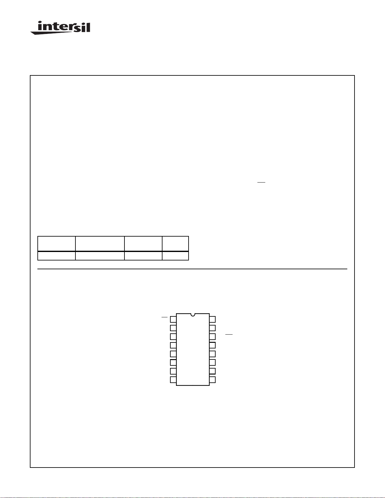
Ordering Information
PART
PACKAGE TEMP. RANGE
SBDIP -55oC to +125oC CDP1821CD3 D16.3
NUMBER PKG. NO.
Description
The CDP1821C/3 is a 1024-word x 1-bit CMOS silicon-on-sapphire (SOS), fully static, random-access memory designed for
use in CDP1800 microprocessor systems. This device has a
recommended operating voltage range of 4V to 6.5V.
The output state of the CDP1821C/3 is a function of the
input address and chip-select states only. Valid data will
appear at the output in one access time following the latest
address change to a selected chip. After valid data appears,
the address may be changed immediately. It is not necessary to clock the chip-select input or any other input terminal
for fully static operation; therefore the chip-select input may
be used as an additional address input. When the device is
in an unselected state (
DD
and output sense amplifier are disabled. This feature allows
the three-state data outputs from many arrays to be OR-tied
to a common bus for easy memory expansion.
CS = 1), the internal write circuitry
Pinout
CS
A0
A1
A2
A3
A4
DO
V
SS
CDP1821C/3
(SBDIP)
TOP VIEW
1
2
3
4
5
6
7
8
16
15
14
13
12
11
10
9
V
DD
DI
RD/WR
A9
A8
A7
A6
A5
CAUTION: These devices are sensitive to electrostatic discharge; follow proper IC Handling Procedures.
http://www.intersil.com or 407-727-9207
| Copyright © Intersil Corporation 1999
6-5
File Number 2983.1
Page 2
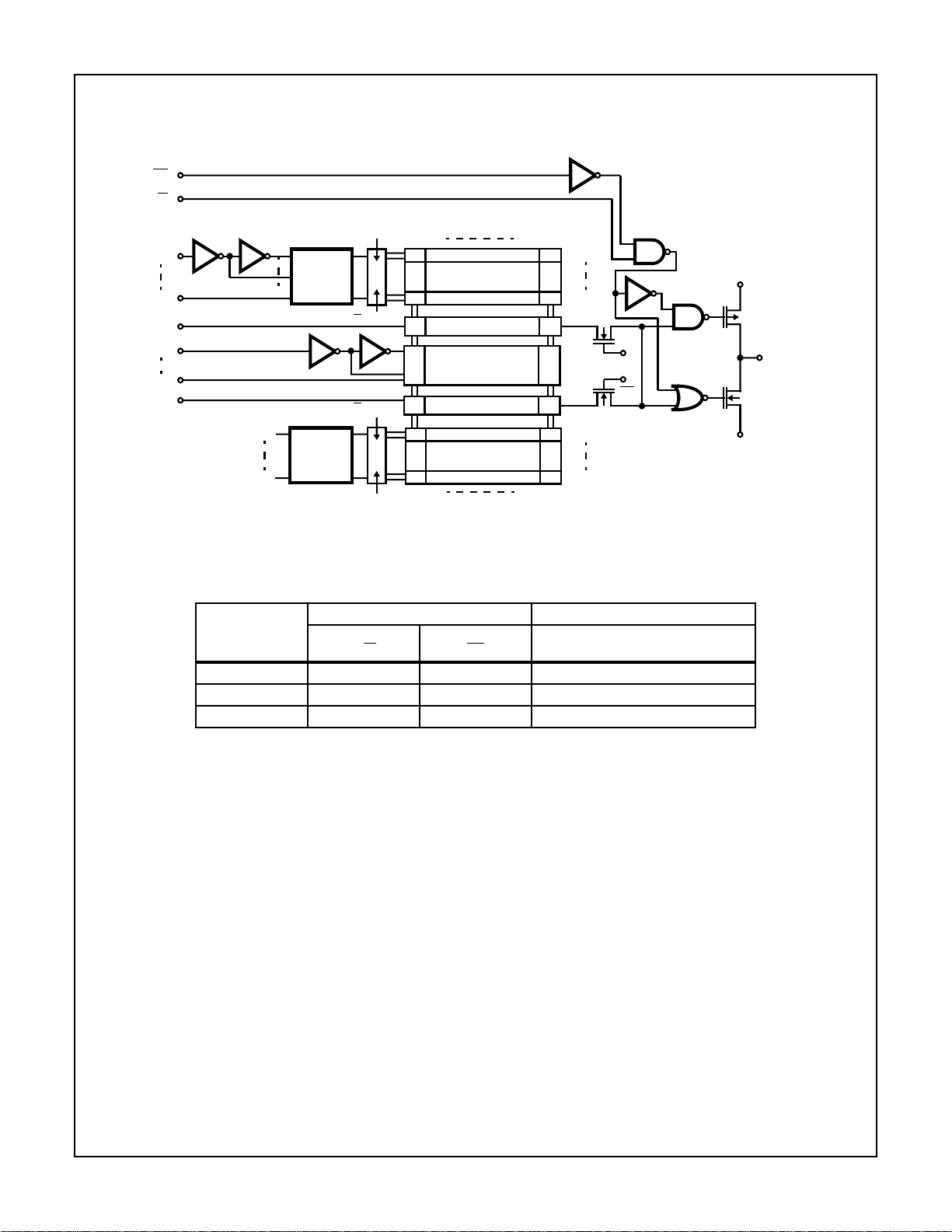
Functional Block Diagram
CS
W
R/
a0
a3
a0
a3
1/16
ROW
DECODER
1/16
ROW
DECODER
A0
A3
DI
A5
A9
DI
ROW
BUFFERS
CS • R/W • A4
CS •
R/W • A4
ROW
BUFFERS
CDP1821C/3
COL. 0 COL. 31
16 x 32
CELL ARRAY
COLUMN BUFFERS
1/32
COLUMN DECODER
COLUMN BUFFERS
16 x 32
CELL ARRAY
COL. 0 COL. 31
ROW 0
ROW 15
ROW 16
ROW 31
A4
A4
V
DD
DO
V
SS
OPERATIONAL MODES
INPUTS OUTPUT
MODE
READ/WRITE
R/W
CHIP-SELECT
CS DATA OUTPUT DO
Standby X 1 High Impedance
Write 0 0 High Impedance
Read 1 0 Contents of Addressed Call
X = Don’t Care Logic 1 = High Logic 0 = Low
6-6
Page 3
CDP1821C/3
Absolute Maximum Ratings Thermal Information
DC Supply Voltage Range, (VDD)
(All Voltages Referenced to VSS Terminal). . . . . . . . -0.5V to +7V
Input Voltage Range, All Inputs . . . . . . . . . . . . . -0.5V to VDD +0.5V
DC Input Current, Any One Input. . . . . . . . . . . . . . . . . . . . . . . . .±10mA
Thermal Resistance (Typical) θJA (oC/W) θJC (oC/W)
SBDIP Package. . . . . . . . . . . . . . . . . . 75 20
Maximum Operating Temperature Range (TA) . . . .-55oC to +125oC
Maximum Storage Temperature Range (T
Maximum Lead Temperature (During Soldering) . . . . . . . . .+265oC
Maximum Junction Temperature . . . . . . . . . . . . . . . . . . . . . . +150oC
) . . .-65oC to +150oC
STG
Recommended Operating Conditions T
= Full Package-Temperature Range. For maximum reliability, nominal operating con-
A
ditions should be selected so that operation is always within the following ranges:
CDP1821CD/3
PARAMETER
DC Operating Voltage Range 4 6.5 V
Input Voltage Range V
Static Electrical Specifications V
= 5V ±5%
DD
SS
V
DD
-55oC, +25oC +125oC
PARAMETER SYMBOL CONDITIONS
Quiescent Device Current (Note 1) I
Output Low Drive (Sink) Current (Note 1) I
Output High Drive (Source) Current
I
DD
OL
OH
VIN = 0V or V
V
OUT
V
OUT
DD
= 0.4V 2.7 - 1.6 - mA
= VDD -0.4V -1.3 - -0.8 - mA
- 260 - 1000 µA
(Note 1)
Output Voltage Low-Level V
Output Voltage High-Level V
OL
OH
- - 0.1 - 0.5 V
-V
-0.1 - VDD -0.5 - V
DD
UNITSMIN MAX
V
UNITSMIN MAX MIN MAX
Input Low Voltage V
Input High Voltage V
Input Current (Note 1) I
Three-State Output Leakage Current
I
IL
IH
IN
OUT
VIN = 0V or V
VIN = 0V or V
- - 0.3 V
- 0.7 V
DD
DD
DD
- 2.6 - 10 µA
- 2.6 - 10 µA
DD
- 0.7 V
- 0.3 V
DD
DD
V
-V
(Note 1)
Operating Current (Note 2) I
Input Capacitance C
Output Capacitance C
DD1
IN
OUT
- - 5 - 10 mA
- - 7.5 - 7.5 pF
- - 15 - 15 pF
NOTES:
1. Limits designate 100% testing. All other limits are designer’s parameters under given test conditions and do not represent 100% testing
2. Measured with 1µs read-cycle time and outputs floating.
6-7
Page 4

CDP1821C/3
Read Cycle Dynamic Electrical Specifications t
, tF = 10ns, CL = 50pF
R
-55oC, +25oC +125oC
V
PARAMETER SYMBOL
Data Access Time (Note 1) t
Read Cycle Time t
Output Enable Time t
Output Disable Time t
DA
RC
EN
DIS
DD
(V)
5 - 190 - 255 ns
5 190 - 255 - ns
5 65 - 90 - ns
5 - 65 - 90 ns
NOTE:
1. 100% testing. All other limits are designer’s parameters under given test conditions and do not represent 100% testing.
t
CS
A0 - A9
R/
(NOTE 3)
DATA OUT
(NOTE 5)
(NOTE 1)
t
RC
W
t
AA
DOA
(NOTE 4)
DATA OUT
VALID
(NOTE 2)
t
DOH
(NOTE 5)
HIGH
IMPEDANCE
UNITSMIN MAX MIN MAX
NOTES:
1. Chip-Select (CS) permitted to change from high to low level or remain low on a selected device.
2. Chip-Select (CS) permitted to change from low to high level or remain low.
3. Read/Write (R/W) must be at a high level during all address transitions.
4. Don’t care.
5. Data-Out (DO) is a high impedance within t
ns after the falling edge of R/W or the rising edge of CS.
DIS
FIGURE 1. READ CYCLE TIMING DIAGRAM
6-8
Page 5

CDP1821C/3
Write Cycle Dynamic Electrical Specifications t
, tF = 10ns, CL = 50pF
R
-55oC, +25oC +125oC
V
PARAMETER SYMBOL
Write Cycle Time t
Address Setup Time (Note 1) t
Address Hold Time (Note1) t
Input Data Setup Time (Note 1) t
Input Data Hold Time (Note 1) t
Read/Write Pulse Width Low (Note 1) t
WC
AS
AH
DS
DH
WL
DD
(V)
5 300 - 420 - ns
5 60 - 84 - ns
5 130 - 180 - ns
5 90 - 125 - ns
5 60 - 84 - ns
5 110 - 155 - ns
NOTE:
1. 100% testing. All other limits are designer’s parameters under given test conditions and do not represent 100% testing.
CS
A0 - A9
(NOTE 1)
t
WC
(NOTE 2)
UNITSMIN MAX MIN MAX
t
WL
W
R/
(NOTE 3)
t
AS
t
DS
t
AH
t
DH
NOTES:
1. Chip-Select (CS) permitted to change from high to low level or remain low on a selected device.
2. Chip-Select (CS) permitted to change from low to high level or remain low.
3. Don’t care.
FIGURE 2. WRITE CYCLE TIMING DIAGRAM
(NOTE 3)(NOTE 3)DI
6-9
Page 6

Data Retention Specifications
CDP1821C/3
TEST CONDITIONS -55oC, +25oC +125oC
PARAMETER SYMBOL
Minimum Data Retention Voltage
V
DR
(V)
V
DD
- - - 2 - 2.5 V
V
DD
(V) MIN MAX MIN MAX
(Note 1)
Data Retention Quiescent Current
I
DD
2 - - 50 - 200 µA
(Note 1)
Chip Deselect to Data Retention Time t
Recovery to Normal Operation Time t
CDR
RC
- 5 450 - 650 - ns
- 5 450 - 650 - ns
NOTE:
1. 100% testing. All other limits are designer’s parameters under given test conditions and do not represent 100% testing
DATA RETENTION MODE
V
DD
0.95 V
t
R
DD
t
RC
V
IH
V
IL
t
CDR
V
CS
0.95 V
DD
VDR
t
F
V
IH
IL
UNITS
FIGURE 3. LOW VDD DATA RETENTION WAVEFORMS AND TIMING DIAGRAM
Burn-In Circuit
R
A11
A0
A1
A2
A3
A4
VDD/2
R
I
R = 8.2kΩ 20%
R
= 2kΩ 20%
I
PACKAGE V
1
R
2
R
3
R
4
R
5
R
6
7
8
TEMPERATURE DURATION
DD
D 7V +125oC 160 Hrs.
FIGURE 4. DYNAMIC/OPERATING BURN-IN CIRCUIT AND TIMING DIAGRAM
16
R
15
R
14
R
13
R
12
R
11
R
10
R
9
V
A10
O1
A9
A8
A7
A6
A5
DD
0 1.6 2.2 5.0 6.6 7.2 10.0
O1
A0
A1
A1 - A11 ARE DIVISION BY 2 BASED ON A0
µs
V
DD
0
V
DD
0
V
DD
0
6-10
Page 7

CDP1821C/3
All Intersil semiconductor products are manufactured, assembled and tested under ISO9000 quality systems certification.
Intersil products are sold by description only. Intersil Corporation reserves the right to make changes in circuit design and/or specifications at any time without
notice. Accordingly, the reader is cautioned to verify that data sheets are current before placing orders. Information furnished by Intersil is believed to be accurate
and reliable. However, no responsibility is assumed by Intersil or its subsidiaries for its use; nor for any infringements of patents or other rights of third parties which
may result from its use. No license is granted by implication or otherwise under an y patent or patent rights of Intersil or its subsidiaries.
For information regarding Intersil Corporation and its products, see web site http://www.intersil.com
Sales Office Headquarters
NORTH AMERICA
Intersil Corporation
P. O. Box 883, Mail Stop 53-204
Melbourne, FL 32902
TEL: (407) 724-7000
FAX: (407) 724-7240
EUROPE
Intersil SA
Mercure Center
100, Rue de la Fusee
1130 Brussels, Belgium
TEL: (32) 2.724.2111
FAX: (32) 2.724.22.05
6-11
ASIA
Intersil (Taiwan) Ltd.
Taiwan Limited
7F-6, No. 101 Fu Hsing North Road
Taipei, Taiwan
Republic of China
TEL: (886) 2 2716 9310
FAX: (886) 2 2715 3029
 Loading...