

Page 1
3-30
March 1997
CDP1802AC/3
High-Reliability CMOS 8-Bit Microprocessor
Features
• For Use In Aerospace, Military, and Critical Industrial
Equipment
• Minimum Instruction Fetch
-Execute Time of 4.5µs
(Maximum ClockFrequency of 3.6MHz) at V
DD
= 5V , T
A
= +25oC
• Operation Over the Full Military
Temperature Range. . . . . . . . . . . . . . . -55
o
C to +125oC
• Any Combination of Standard RAM and ROM Up to
65,536 Bytes
• 8–Bit Parallel Organization With Bidirectional Data
Bus and Multiplexed Address Bus
• 16 x 16 Matrix of Registers for Use as Multiple Program Counters, Data Pointers, or Data Registers
• On-Chip DMA, Interrupt, and Flag Inputs
• High Noise Immunity. . . . . . . . . . . . . . . . . . 30% of V
DD
Description
The CDP1802A/3 High-Reliability LSI CMOS 8-bit register
oriented Central
-Processing Unit (CPU) is designed for use
as a general purpose computing or control element in a wide
range of stored
-program systems or products.
The CDP1802A/3 includes all of the circuits required for
fetching, interpreting, and executing instructions which have
been stored in standard types of memories. Extensive
input/output (I/O) control features are also provided to facilitate system design.
The 1800 Series Architecture is designed with emphasis on
the total microcomputer system as an integral entity so that
systems having maximum flexibility and minimum cost can be
realized. The 1800 Series CPU also provides a synchronous
interface to memories and external controllers for I/O devices,
and minimizes the cost of interface controllers. Further, the I/O
interface is capable of supporting devices operating in polled,
interrupt
-driven, or direct memory-access modes.
The CDP1802AC/3 is functionally identical to its predecessor, the CDP1802. The “A” version includes some performance enhancements and can be used as a direct
replacement in systems using the CDP1802.
This type is supplied in 40 lead dual
-in-line sidebrazed
ceramic packages (D suffix).
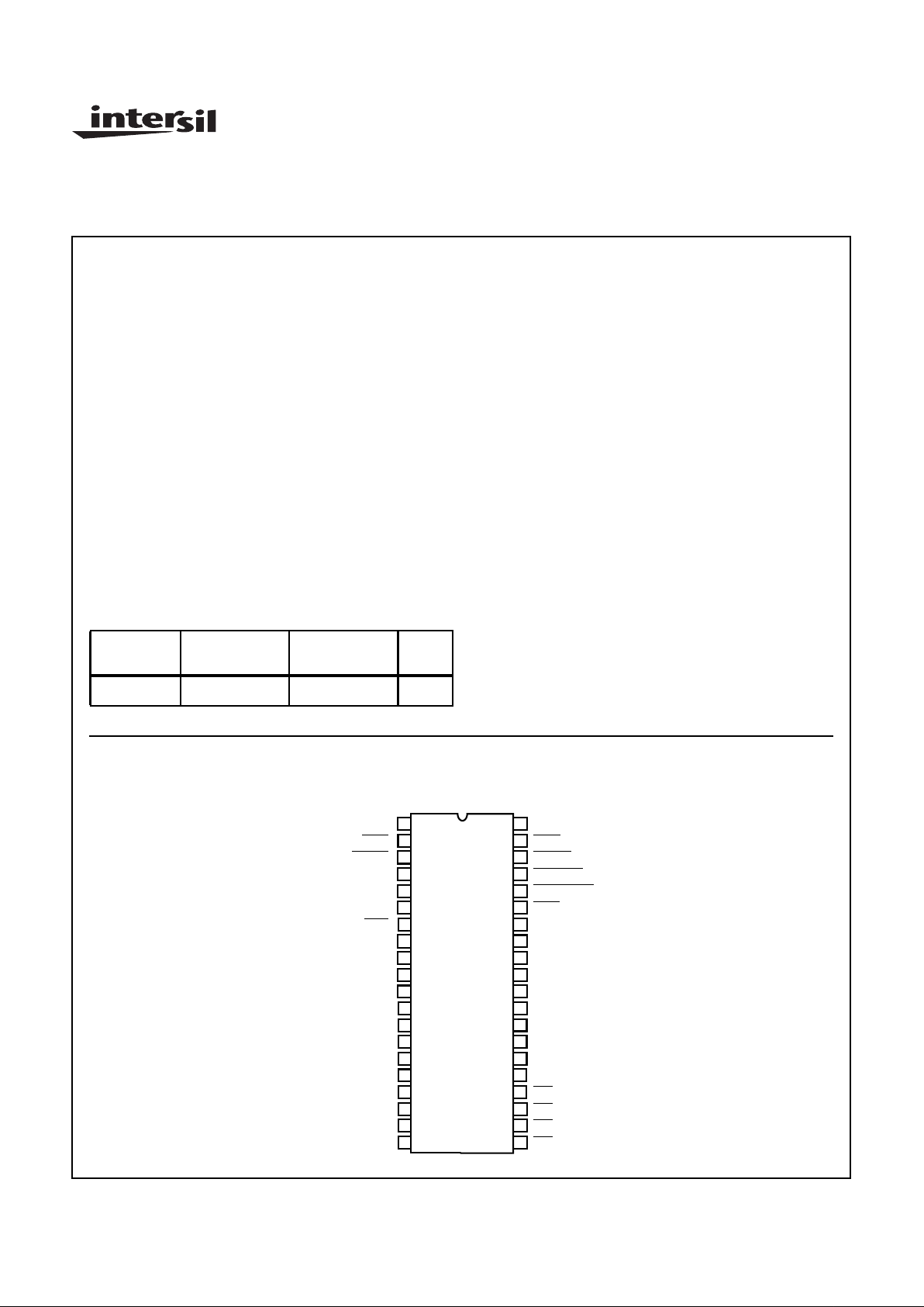
Pinout
CDP1802AC/3 (SBDIP)
TOP VIEW
Ordering Information
PACKAGE
TEMP. RANGE
(oC) 5V - 3.2MHz
PKG
NO.
SBDIP -55 to 125 CDP1802ACD3 D40.6
13
1
2
3
4
5
6
7
8
9
10
11
12
14
15
16
17
18
19
20
CLOCK
WAIT
CLEAR
Q
SC1
SC0
MRD
BUS 7
BUS 6
BUS 5
BUS 4
BUS 3
BUS 2
BUS 1
BUS 0
V
CC
N2
N1
N0
V
SS
28
40
39
38
37
36
35
34
33
32
31
30
29
27
26
25
24
23
22
21
V
DD
XTAL
DMA IN
DMA OUT
INTERRUPT
MWR
TPA
TPB
MA7
MA6
MA5
MA4
MA3
MA2
MA1
MA0
EF1
EF2
EF3
EF4
File Number 1441.2
CAUTION: These devices are sensitive to electrostatic discharge; follow proper IC Handling Procedures.
http://www.intersil.com or 407-727-9207
| Copyright © Intersil Corporation 1999
[ /Title
(CDP1
802AC
/
3)
/
Sub-
j
ect
(HighReliability
CMOS
8-Bit
Microprocessor)
/
Autho
r ()
/
Keywords
(Intersil
Corporation,
8-bit
microprocessors, 8
bit
microprocessors,
peripherals)
/
Creator ()
/
DOCI
NFO
pdfmark
Page 2
3-31
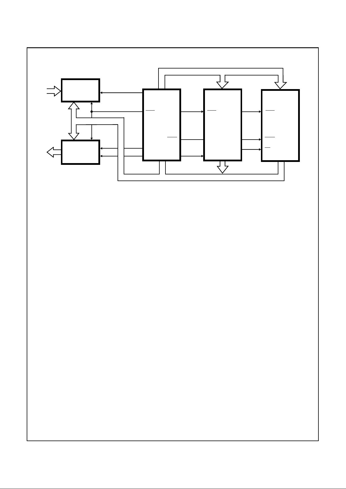
CDP1852
INPUT PORT
DAT A
CS1
CS2
CDP1852
OUTPUT
PORT
CLOCK
CS1
CS2
MA0–7
N0
MRD
MWR
N1
TPB DATA TPA
CDP1802
8–BIT CPU
MRD
MA0–4
MWR
CS
CDP1824
32 BYTE RAM
MA0–7
DAT A
CEO
TPA
MRD
8–BIT DATA BUS
ADDRESS BUS
CDP1833
1K–ROM
DATA
FIGURE 1. TYPICAL CDP1802A/3 SMALL MICROPROCESSOR SYSTEM
CDP1802AC/3
Page 3
3-32
Absolute Maximum Ratings Thermal Information
DC Supply Voltage Range, (VDD)
(All Voltages Referenced to VSS Terminal)
CDP1802AC/3 . . . . . . . . . . . . . . . . . . . . . . . . . . . . . . -0.5V to +7V
Input Voltage Range, All Inputs . . . . . . . . . . . . . -0.5V to VDD +0.5V
DC Input Current, any One Input. . . . . . . . . . . . . . . . . . . . . . . . .±10mA
Thermal Resistance (Typical) θJA (oC/W) θJC (oC/W)
SBDIP Package. . . . . . . . . . . . . . . . . . . . 55 15
Device Dissipation Per Output Transistor
TA = Full Package Temperature Range. . . . . . . . . . . . . . . . . 100mW
Operating Temperature Range (TA)
Package Type D. . . . . . . . . . . . . . . . . . . . . . . . . .-55oC to +125oC
Storage Temperature Range (T
STG
). . . . . . . . . . . .-65oC to +150oC
Lead Temperature (During Soldering)
At distance 1/16 ±1/32 In. (1.59 ±0.79mm)
from case for 10s max . . . . . . . . . . . . . . . . . . . . . . . . . . . +265oC
CAUTION: Stresses above those listed in “Absolute Maximum Ratings” may cause permanent damage to the device. This is a stress only rating and operation
of the device at these or any other conditions above those indicated in the operational sections of this specification is not implied.
Recommended Operating Conditions T
A
= Full Package Temperature Range. For maximum reliability, operating conditions
should be selected so that operation is always within the following ranges
PARAMETER MIN MAX UNITS
DC Operating Voltage Range 4 6.5 V
Input Voltage Range V
SS
V
DD
V
Maximum Clock Input Rise or Fall Time - 1 µs
Performance Specifications
PARAMETER VDD (V) -55oC TO +25oC +125oC UNITS
Minimum Instruction Time (Note 1) 5 4.5 5.9 µs
Maximum DMA Transfer Rate 5 450 340 Kbytes/s
Maximum Clock Input Frequency,
Load Capacitance (CL) = 50pF, f
CL
5 DC-3.6 DC-2.7 MHz
NOTE:
1. Equals 2 machine cycles - one Fetch and one Execute operation for all instructions except Long Branch and Long Skip, which require 3
machine cycles - one Fetch and two Execute operations.
Static Electrical Specifications All Limits are 100% Tested
PARAMETER
CONDITIONS -55oC, +25oC +125oC
UNITS
V
OUT
(V) V
IN,
(V) V
CC,VDD
(V) MIN MAX MIN MAX
Quiescent Device Current, I
DD
- - 5 - 100 - 250 µA
Output Low Drive (Sink) Current
(Except XTAL), I
OL
0.4 0, 5 5 1.20 - 0.90 - mA
XTAL 0.4 5 5 185 - 140 - µA
Output High Drive (Source)
Current (Except XTAL), I
OH
4.6 0, 5 5 - -0.30 - -0.20 mA
XTAL 4.6 0 5 - -135 - -100 µA
Output Voltage Low-Level, V
OL
- 0, 5 5 - 0.1 - 0.2 V
Output Voltage High-Level, V
OH
- 0, 5 5 4.9 - 4.8 - V
CDP1802AC/3
Page 4

3-33
Input Low Voltage, V
IL
0.5, 4.5 - 5 - 1.5 - 1.5 V
Input High Voltage, V
IH
0.5, 4.5 - 5 3.5 - 3.5 - V
Input Leakage Current, I
IN
Any
Input
0, 5 5 - ±1-±5 µA
Three-State Output Leakage
Current, I
OUT
0, 5 0, 5 5 - ±1-±5 µA
NOTE:
2. 5V level characteristics apply to Part No. CDP1802AC/3, and 5V and 10V level characteristics apply to part No. CDP1802A/3.
Timing Specifications As a Function of T (T = 1/fCLOCK), C
L
= 50 pF
PARAMETER VDD (V)
LIMITS (NOTE 3)
-55oC, +25oC +125oC UNITS
High-Order Memory-Address Byte Setup to TPA Time, t
SU
5 2T-450 2T-580 ns
High-Order Memory-Address Byte Hold After TPA Time, t
H
5 T/2 +0 T/2 +0 ns
Low-Order Memory-Address Byte Hold After WR Time, t
H
5 T-30 T-40 ns
CPU Data to Bus Hold After WR Time, t
H
5 T-170 T-250 ns
Required Memory Access Time Address to Data, t
ACC
5 5T-300 5T-400 ns
NOTE:
3. These limits are not directly tested.
Implicit Specifications (Note 4) T
A
= -55oC to +25oC
PARAMETER SYMBOL VDD (V)
TYPICAL
VALUES UNITS
Typical Total Power Dissipation
Idle “00” at M(0000), CL = 50pF
f = 2MHz - 5 4 mW
Effective Input Capacitance any Input - C
IN
-5pF
Effective Three-State Terminal Capacitance Data Bus - - 7.5 pF
Minimum Data Retention Voltage - V
DR
- 2.4 V
Data Retention Current - I
DR
2.4 10 µA
NOTE:
4. These specifications are not tested. Typical values are provided for guidance only.
Static Electrical Specifications All Limits are 100% Tested (Continued)
PARAMETER
CONDITIONS -55oC, +25oC +125oC
UNITS
V
OUT
(V) V
IN,
(V) V
CC,VDD
(V) MIN MAX MIN MAX
CDP1802AC/3
Page 5

3-34
Dynamic Electrical Specifications C
L
= 50pF, Timing Measurement at 0.5 VDD Point
PARAMETERS VDD (V)
-55oC TO +25oC +125oC
UNITSMIN MAX MIN MAX
Progagation Delay Times, t
PLH
, t
PHL
Clock to TPA, TPB 5 - 275 - 370 ns
Clock-to-Memory High Address Byte, t
PLH
, t
PHL
5 - 725 - 950 ns
Clock-to-Memory Low Address Byte Valid, t
PLH
, t
PHL
5 - 340 - 425 ns
Clock to MRD, t
PLH
, t
PHL
5 - 340 - 425 ns
Clock to MWR,t
PLH
, t
PHL
5 - 275 - 370 ns
Clock to (CPU DATA to BUS) Valid, t
PLH
, t
PHL
5 - 430 - 550 ns
Clock to State Code, t
PLH
, t
PHL
5 - 440 - 550 ns
Clock to Q, t
PLH
, t
PHL
5 - 375 - 475 ns
Clock to N (0 - 2), t
PLH
, t
PHL
5 - 400 - 525 ns
Interface Timing Requirements (Note 5)
Data Bus Input Setup, t
SU
5 10 - 10 - ns
Data Bus Input Hold, t
H
5 175 - 230 - ns
DMA Setup, t
SU
5 10 - 10 - ns
DMA Hold, t
H
5 200 - 270 - ns
Interrupt Setup, t
SU
5 10 - 10 - ns
Interrupt Hold, t
H
5 175 - 230 - ns
WAIT Setup, t
SU
5 30 - 30 - ns
EF1-4 Setup, t
SU
5 20 - 20 - ns
EF1-4 Hold, t
H
5 100 - 135 - ns
Required Pulse Width Times
CLEAR Pulse Width, t
WL
5 150 - 200 - ns
CLOCK Pulse Width, t
WL
5 140 - 185 - ns
NOTE:
5. Minimum input setup and hold times required by Part CDP1802AC/3.
CDP1802AC/3
Page 6

3-35
NOTES:
6. This timing diagram is used to show signal relationships only, and does not represent any specific machine cycle.
7. All measurements are referenced to 50% point of the waveforms.
8. Shaded areas indicate “don’t care” or undefined state. Multiple transitions may occur during this period.
FIGURE 2. TIMING WAVEFORMS
0 2 3 4 5 6 7 0
00 10 20 30 40 50 60 70 00
01 11 21 31 41 51 61 71 01
t
W
CLOCK
t
PLH
t
PHL
TPA
TPB
t
SU
t
H
t
PLH
t
PHL
t
PLH,tPHL
LOW ORDER
ADDRESS BYTE
MEMORY
ADDRESS
t
PLH
MRD
(MEMORY
READ CYCLE)
t
PHL
t
PLH
t
PLH
t
PHL
t
PHL
MWR
(MEMORY
WRITE CYCLE)
DATA FROM
CPU TO BUS
STATE
CODES
t
PLH
t
PHL
t
PLH
t
PHL
Q
t
PLH,tPHL
N0, N1, N2
(I/O
EXECUTION
CYCLE)
t
PLH
DAT A
LATCHED IN CPU
DATA FROM
BUS TO CPU
t
H
DMA
INTERRUPT
SAMPLED (S1, S2)
t
SUtH
t
SUtH
DMA
REQUEST
INTERRUPT
REQUEST
FLAG LINES
SAMPLED (IN SI)
EF 1-4
t
SUtH
WAIT
CLEAR
t
W
t
SU
ANY NEGATIVE
TRANSITION
t
PLH,tPHL
t
PLH
t
PHL
SAMPLED (S1, S2, S3)
t
SU
1
HIGH ORDER
ADDRESS BYTE
t
PLH,tPHL
t
PLH,tPHL
CDP1802AC/3
Page 7

3-36
Performance Curves
FIGURE 3. TYPICAL MAXIMUM CLOCK FREQUENCY AS A
FUNCTION OF TEMPERATURE
FIGURE 4. TYPICAL MAXIMUM CLOCK FREQUENCY AS A
FUNCTION OF SUPPLY VOLTAGE
FIGURE 5. TYPICAL TRANSITION TIME vs LOAD
CAPACITANCE
FIGURE 6. MINIMUM OUTPUT HIGH (SOURCE) CURRENT
CHARACTERISTICS
FIGURE 7. MINIMUM OUTPUT LOW (SINK) CURRENT
CHARACTERISTICS
NOTES:
9. Idle = “00” at M (0000)
10. Branch = “3707” at M (8107)
FIGURE 8. TYPICAL POWER DISSIPATION AS A FUNCTION
OF CLOCK FREQUENCY FOR BRANCH
INSTRUCTION AND IDLE INSTRUCTION
5
4
3
2
1
0
6
7
8
35 45 55 65 75 85 95 105 11525 125
SYSTEM MAXIMUM CLOCK FREQUENCY
(f
CL
) (MHz)
VDD = 5V
LOAD CAPACITANCE (CL) = 50pF
AMBIENT TEMPERATURE (T
A
) (oC)
345678910 122
SUPPLY VOLTAGE (V
DD
) (V)
11
5
4
3
2
1
0
6
7
SYSTEM MAXIMUM CLOCK FREQUENCY
(f
CL
) (MHz)
8
LOAD CAPACITANCE (CL) = 50pF
TA = 25oC
TA = 125oC
EXTRAPOLA
TED
50 75 100 125 150 175 20025
300
250
200
150
100
350
400
0
50
TRANSITION TIME (t
THL
, t
TLH
) (ns)
AMBIENT TEMPERATURE (TA) = 25oC
0
LOAD CAPACITANCE (C
L
) (pF)
t
TLH
t
THL
-9 -8 -7 -6 -5 -4 -3-10
2
3
4
5
6
1
0-2 -1
OUTPUT HIGH (SOURCE) CURRENT
(I
OH
-mA)
DRAIN TO SOURCE VOLTAGE (VDS) (V)
GATE TO SOURCE VOLTAGE (VGS) = -5V
AMBIENT TEMPERATURE = -40 TO +85oC
0
25
20
15
10
5
30
35
123456708910
GATE TO SOURCE VOLTAGE (VGS) = 5V
AMBIENT TEMPERATURE = -40oC TO +85oC
OUTPUT LOW (SINK) CURRENT (I
OL
) (mA)
0
DRAIN-TO-SOURCE VOLTAGE (V
DS
) (V)
10
1
0.1
100
1000
0.01 0.1 1 10
AMBIENT TEMPERATURE (TA) = 25oC
CLOCK INPUT FREQUENCY (f
CL
) (MHz)
TYPICAL POWER DISSIPATION
(P
D
) (mW)
V
CC
= V
DD
= +5V
V
CC
= V
DD
= 5V
“BRANCH”
“IDLE”
CDP1802AC/3
Page 8

3-37
All Intersil semiconductor products are manufactured, assembled and tested under ISO9000 quality systems certification.
Intersil products are sold by description only. Intersil Corporation reserves the right to make changes in circuit design and/or specifications at any time without
notice. Accordingly, the reader is cautioned to verify that data sheets are current before placing orders. Information furnished by Intersil is believed to be accurate
and reliable. However, no responsibility is assumed by Intersil or its subsidiaries for its use; nor for any infringements of patents or other rights of third parties which
may result from its use. No license is granted by implication or otherwise under an y patent or patent rights of Intersil or its subsidiaries.
For information regarding Intersil Corporation and its products, see web site http://www.intersil.com
Burn-In Circuit
NOTE: Any output except XTAL.
FIGURE 9. TYPICAL CHANGE IN PROPAGATION DELAY AS A FUNCTION OF A CHANGE IN LOAD CAPACITANCE
TYPE V
DD
TEMPERATURE TIME
CDP1802AC 7V +125oC 160 Hours
FIGURE 10. BIAS/STATIC BURN-IN CIRCUIT
Performance Curves
(Continued)
100
75
50
25
0
125
150
∆ PROPAGATION DELAY TIME
(∆t
PLH
, ∆t
PHL
) (ns)
50 100 150 2000
∆ LOAD CAPACITANCE (∆C
L
) (pF)
AMBIENT TEMPERATURE
(T
A
) = 25oC
V
CC
= V
DD
= 5V
∆
t
PHL
∆
t
PLH
V
CC
= V
DD
= 5V
V
DD
V
DD
NC
NC
V
DD
V
DD
NC
13
1
2
3
4
5
6
7
8
9
10
11
12
14
15
16
17
18
19
20
28
40
39
38
37
36
35
34
33
32
31
30
29
27
26
25
24
23
22
21
ALL RESISTORS ARE 47kΩ±20%
CDP1802AC/3
 Loading...