

Page 1
CD-G15000/CP-G15000S
In the interests of user-safety the set should be restored to its
origina
l condition and only parts identical to those specified be
used
.
SERVICE MANUAL
No.S2605CDG15000
MINI COMPONENT SYSTEM
CONTENTS
PRECAUTIONS FOR USING LEAD FREE SOLDER
CHAPTER 1. GENERAL DESCRIPTION
[1] Important service notes ................................1-1
[2] Specifications.................................................1-2
[3] Names of parts ..............................................1-3
CHAPTER 2. ADJUSTMENTS
[1] Mechanism section........................................2-1
[2] Test mode ......................................................2-2
[3] CD section .....................................................2-4
[4] CD Changer mechanism section ...................2-5
CHAPTER 3. MECHANISM BLOCKS
[1] Caution on disassembly ................................3-1
Removing and reinstalling the main parts ........3-4
[2]
CHAPTER 4. DIAGRAMS
[1] CD Block diagrams........................................4-1
[2] Main Block diagrams .....................................4-2
[3] Sub Woofer Block diagram............................4-3
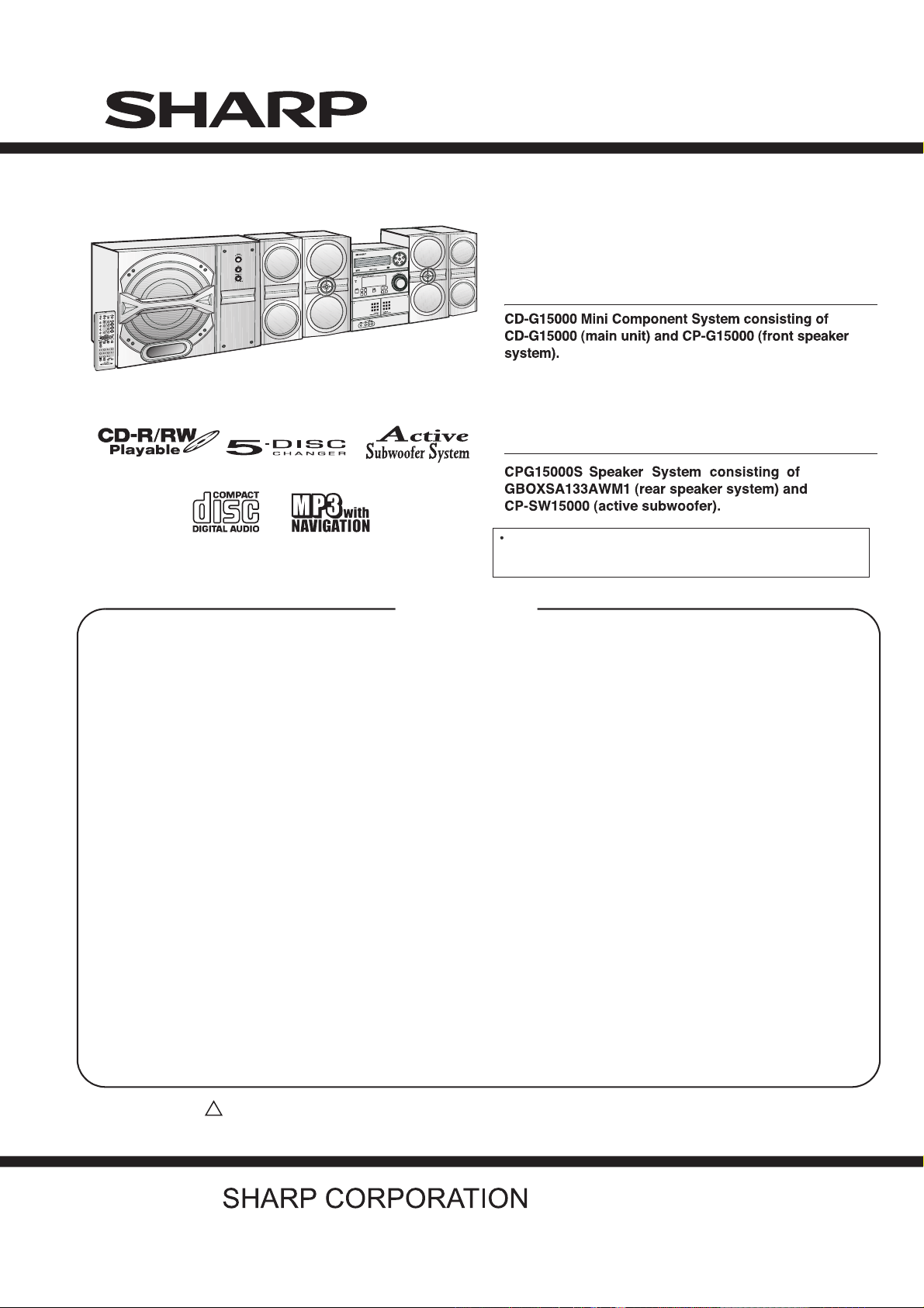
MODEL
CD-G15000
SPEAKER SYSTEM
CP-G15000SMODEL
CHAPTER 6. CIRCUIT SCHEMATICS AND PARTS
LAYOUT
[1] Notes on schematic diagram.......................... 6-1
[2] Types of transistor and LED.......................... 6-1
[3] Schematic diagram ........................................ 6-2
[4] Wiring side of PWB ...................................... 6-10
CHAPTER 7. FLOWCHART
[1] Troubleshooting ............................................. 7-1
CHAPTER 8. OTHERS
[1] Function table of IC ........................................ 8-1
[2] FL Display ...................................................... 8-8
Parts Guide (CD-G15000)
ts Guide (CP-G15000S)
Par
CHAPTER 5. CIRCUIT DESCRIPTION
[1] Waveforms of CD circuit ................................5-1
[2] Voltage...........................................................5-2
Parts marked with " " are important for maintaining the safety of the set. Be sure to replace these parts with specified ones
for maintaining the safety and performance of the set.
!
– 1
This document has been published to be used
fo
r after sales service only.
Th
e contents are subject to change without notice.
Page 2
CD-G15000/CP-G15000S
AudioXL-MP150Service ManualXLMP150MarketE
PRECAUTIONS FOR USING LEAD-FREE SOLDER
1. Employing lead-free solder
"MAIN,DISPLAY,POWER,GAME INPUT,SPEAKER,CD SERVO,CD MOTOR(PWB ONLY),CD CHANGER MOTOR
B ONLY), SUB WOOFER SPEAKER LED,SUB WOOFER AMP,PRIMARY POWER,LED
(PW
FLASHING,JACK,VOLUME,POWE
The LF symbol indicates lead-free solder, and is attached on the PWB and service manuals.The alphabetical
characte
Example:
r following LF shows the type of lead-free solder.
2. Using lead-free wire solder
When fixing the PWB soldered with the lead-free solder, apply lead-free wire solder. Repairing with
conventiona
l lead wire solder may cause damage or accident due to cracks.
As the melting point of lead-free solder (Sn-Ag-Cu) is higher than the lead wire solder by 40 C, were
commen
solderin
d you to use a dedicated soldring bit,if you are not familiar with how to obtain lead-free wire solder or
g bit,contact our service station or service branch in your area.
3. Soldering
As the melting point of lead-free solder (Sn-Ag-Cu) is about 220 C which is higher than the conventional lead
r by 40 C, and as it has poor solder wettability, you may be apt to keep the soldering bit in contact with the
solde
B for extended period of time. However, since the land may be peeled off or the maximum heat-resistance
PW
temperatur
solderin
Lead-fre
e of parts may be exceeded, remove the bit from the PWB as soon as you confirm the steady
g condition.
e solder contains more tin, and the end of the soldering bit may be easily corrected. Make sure to turn
on and off the power of the bit as required.
If a different type of solder stays on the tip of the soldering bit, it is alloyed with lead-free solder.Clean the bit
r every use of it.
afte
Whe
n the tip of the soldering bit is blackened during use, file it with steel wool or fine sandpaper.
Be careful when replacing parts with polarity indication on the PWB silk.
Lead-fre
PWB-A 92LPWB6529MANS
PWB-B 92LPWB6529DPLS
PWB-
PWB-
PWB-
PWB-
e wire solder for servicing
Ref No.
C
D
E
F
Parts No.
92LPWB6514CDU
92LPWB6230LED
QPWBF0027AWZZ
QPWBF1055AWZ
PWB6512AMPSPWB-H
PWB6512CTRSPWB-J
R SWITCH PWB"of this model employs lead-free solder.
Indicates lead-free solder of tin,silver and copper.
MAIN (A1), POWER (A2)
DISPLAY (B1), GAME INPUT (B2), SPEAKER (B3)
S
CD SERVO
SU
S
CD MOTOR (PWB ONLY)
CD CHANGER MOTOR (PWB ONLY)
Z
SUB WOOFER AMP(H1),PRIMARY POWER(H2),LED FLASHING(H3),JACK(H4)
VOLUME (J1),POWER SWITCH (J2)
Description
B WOOFER SPEAKER LED
– 2
i
Page 3

TO EXPOSED
METAL PARTS
CONNECT TO
KNOWN EARTH
GROUND
TEST PROBE
0.15 mF
1.5 kohms
10 W
VTVM
AC SCALE
CHAPTER 1: GENERAL DESCRIPTION
[1] Important service notes
BEFORE RETURNING THE AUDIO PRODUCT
(Fire & Shock Hazard)
Before returning the audio product to the use r, perform
the following safety checks.
1. Inspect all lead dress to make certain that leads are
not pinched or that hardware is not lodged between
the chassis and other metal parts in the audio product.
2. Inspect all protective devices such as insulating
materials, cabinet, terminal board, adjustment and
compartment covers or shields, mechanical insulators etc.
3. To be sure that no shock hazard exists, check for
leakage current in the following manner.
* Plug the AC line cord directly into a 120 volt AC out-
let.
* Using two clip leads, connect a 1.5 kohm, 10 watt
resistor paralleled by a 0.15 µF capacitor in series
with all exposed metal cabinet parts and a known
earth ground, such as conduit or electrical ground
connected to earth ground.
* Use a VTVM or VOM with 1000 ohm per volt, or
higher, sensitivity to measure the AC voltage drop
across the resistor (See diagram).
* Connect the resistor connection to all exposed metal
parts having a return path to the chassis (antenna,
metal cabinet, screw heads, knobs and control
shafts, escutcheon, etc.) and measure the AC voltage drop across the resistor.
CD-G15000/CP-G15000S
All check must be repeated with the AC line cord plug
connection reversed.
Any reading of 0.3 volt RMS (this corresponds to 0.2
milliamp. AC.) or more is excessive and indicates a
potential shock hazard which must be corrected
before returning the audio product to the owner.
1 – 1
– 3
Page 4
CD-G15000/CP-G15000S
[2] Specifications
FOR A COMPLETE DESCRIPTION OF THE OPERATION OF THIS UNIT, PLEASE REFER
TO THE OPERATION MANUAL.
As part of our policy of continuous improvement,
SHARP reserves the right to make design and
specifcation changes for product improvement
without prior notice. The performance specification
figures indicated are nominal values of production
units .There maybe some deviations from these
values in individual units.
CD-G15000 CP-G15000
■ General
Power source AC 120 V, 60 Hz
Power consumption 175 W
Dimensions Width: 10-1/4" (260 mm)
Height: 13" (330 mm)
Depth: 12-7/8" (322 mm)
Weight 21.35 lbs. (9.67 kg)
■ CD player
Type 5-disc multi-play compact disc player
Signal readout Non-contact, 3-beam semiconductor laser
pickup
D/A converter 1-bit D/A converter
Frequency response 20 - 20,000 Hz
Dynamic range 90 dB (1 kHz)
■ Amplifier
Output power
Front speakers 150 watts minimum RMS per channel into
8 ohms from 100 Hz to 20 kHz, 10% total
harmonic distortion
Rear speakers 75 watts minimum RMS per channel into
16 ohms from 5 kHz to 20 kHz, 10% total
harmonic distortion
Output terminals Front speakers: 8 ohms
Rear speakers: 16 ohms
Headphones: 16 - 50 ohms
(recommended: 32 ohms)
Subwoofer pre-out (audio signal):
200 mV/10 k ohms at 70 Hz
Video output: 1Vp-p (75 ohms)
Input terminals Game/Auxiliary (audio signal):
500 mV/47 k ohms
Game/Video: 1Vp-p (75 ohms)
■ Tuner
Frequency range FM: 87.5 - 108.0 MHz
AM: 530 - 1,720 kHz
■ Cassette deck
Frequency response 50 - 14,000 Hz (normal tape)
Signal/noise ratio 55 dB (TAPE-1 playback)
50 dB (TAPE-2 recording/playback)
Wow and flutter 0.3 % (WRMS)
Type 2-way type speaker system
Maximum input
power
Rated input power 150 W
Impedance 8 ohms
Dimensions Width: 7-11/16" (195 mm)
Weight 10.8 lbs. (4.9 kg)/each
Type Full-range speaker system
Maximum input
power
Rated input power 75 W
Impedance 16 ohms
Dimensions Width: 5-11/16" (145 mm)
Weight 6.4 lbs. (2.9 kg)/each
Power source AC 120 V, 60 Hz
Power
consumption
Output power 400 watts minimum RMS into 6 ohms from
Input terminals Subwoofer input (audio signal):
Speaker type 10" (25 cm) woofer
Impedance 6 ohms
Dimensions Width: 18-1/8" (460 mm)
Weight 46.2 lbs. (21 kg)
Specifications for this model are subject to change without prior
notice.
2" (5 cm) tweeter x 1
5-1/8" (13 cm) woofer x 2
300 W
Height: 15-3/4" (400 mm)
Depth: 9-5/8" (244 mm)
GBOXSA133AWM1
4" (10 cm) speaker x 2
150 W
Height: 15-3/4" (400 mm)
Depth: 9-1/8" (231 mm)
CP-SW15000
120 W
50 Hz to 120 Hz, 10% total harmonic
distortion
200mV / 10 k ohms at 70 Hz
Height: 15-3/4" (400 mm)
Depth: 15-13/16" (402 mm)
– 3
1 – 2
Page 5
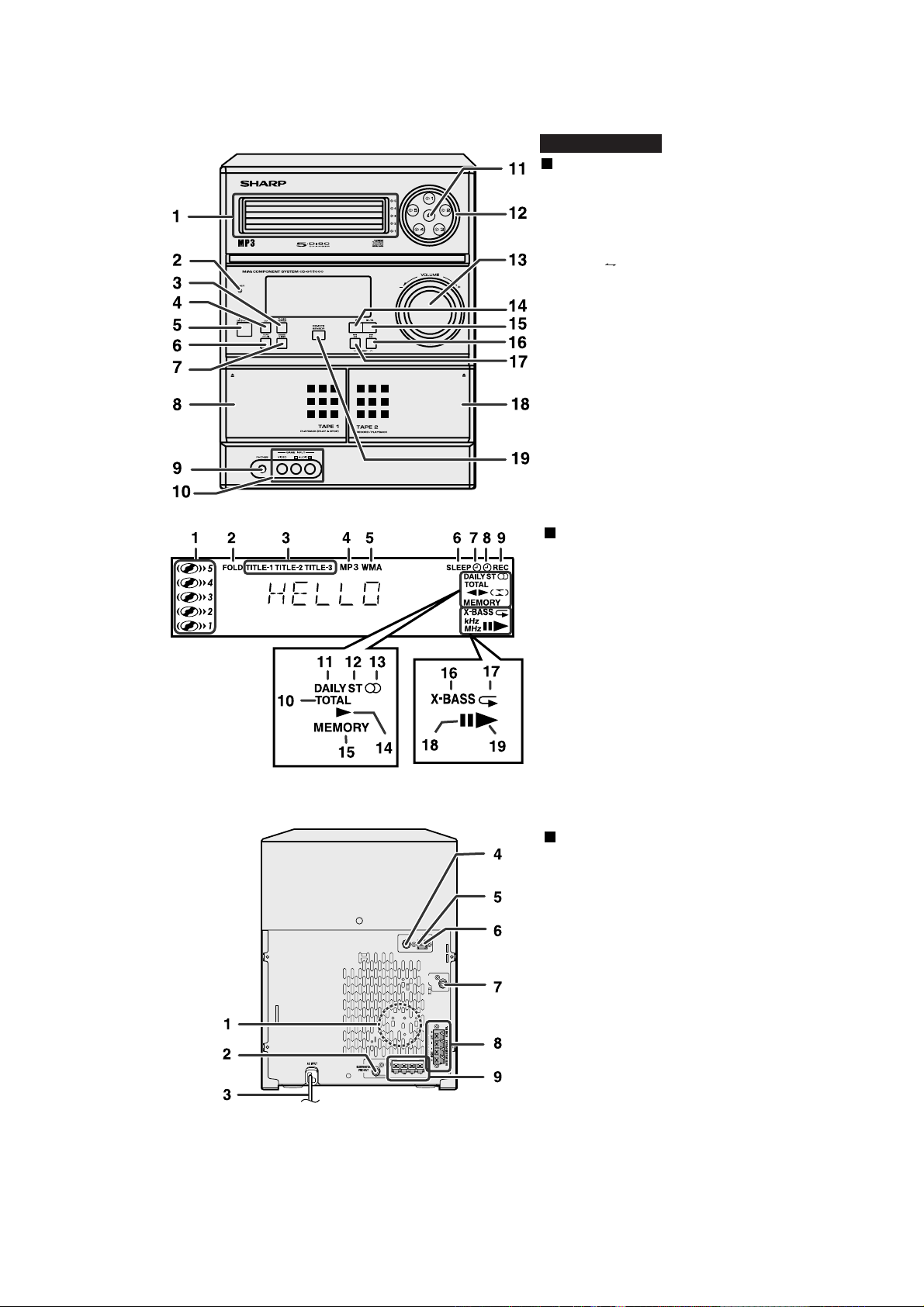
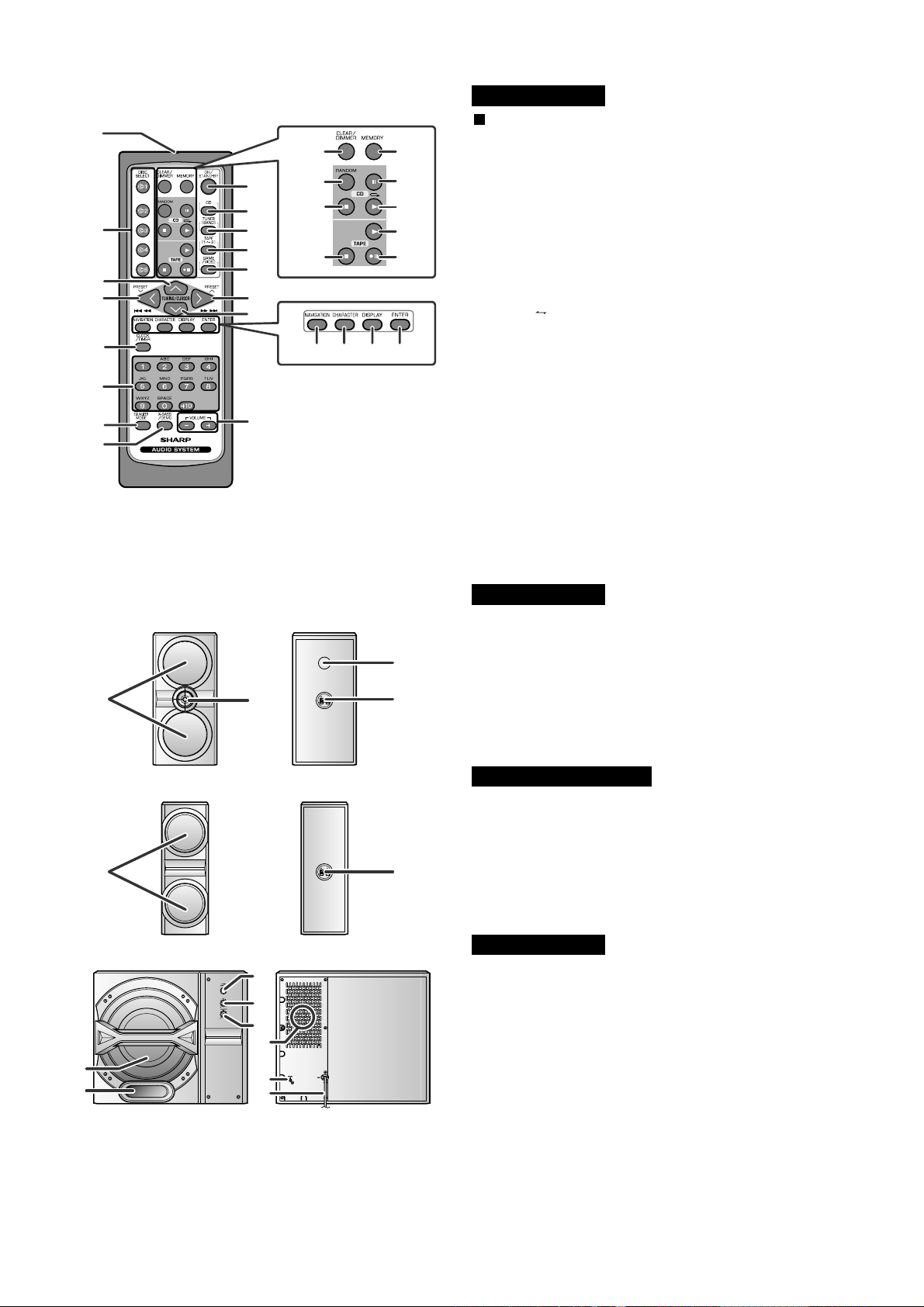
[3] Names of parts
CD-G15000/CP-G15000S
CD-G15000
Front panel
1. Disc Trays
2. Timer Indicator
3. Tuner (Band) Button
4. CD Button
5. Power On/Stand-by Button
6. Tape (1 2) Button
7. Game/Video Button
8. Tape 1 Cassette Compartment
9. Headphone Jack
10. Game/Video Input Jacks
11. Disc Tray Open/Close Button
12. Disc Number Select Buttons
13. Volume Control
14. CD or Tape Stop Button
15. CD Play or Repeat, Tape Play Button
16. CD Track Up or Fast Forward, Tape 2 Fast Forward,
Tuner Preset Up, Time Up Button
17. CD Track Down or Fast Reverse, Tape 2 Rewind,
Tuner Preset Down, Time Down Button
18. Tape 2 Cassette Compartment
19. Remote Sensor
FM GND AM
75OHMS
ANTENNA
Display
1. Disc Number Indicators
2. MP3/WMA Folder Indicator
3. MP3/WMA Title Indicators
4. MP3 Indicator
5. WMA Indicator
6. Sleep Indicator
7. Timer Play Indicator
8. Timer Recording Indicator
9. Tape 2 Record Indicator
10. MP3/WMA Total Indicator
11. Daily Timer Indicator
12. FM Stereo Mode Indicator
13. FM Stereo Receiving Indicator
14. Tape Forward Play Indicator
15. Memory Indicator
16. Extra Bass Indicator
17. Disc Repeat Play Indicator
18. Disc Pause Indicator
19. Disc Play Indicator
Rear panel
1. Cooling Fan
2. Subwoofer Pre-output Jack
3. AC Power Cord
4. FM 75 Ohms Antenna Jack
5. AM Antenna Ground Terminal
6. AM Loop Antenna Terminal
7. Video Output Jack
8. Front Speaker Terminals
VIDEO
OUT
9. Rear Speaker Terminals
REARSPEAKERS
RIGHT
LEFT
RATEDSPEAKERIMPEDANCE:16OHMSMIN.
1 – 3
–2
Page 6
CD-G15000/CP-G15000S
1
2
3
4
5
6
7
8
9
10
11
12
13
14
15
16
17
18
19
20
26
27
28
29
21
22
23
24
25
CD-G15000
Remote control
1. Remote Contr ol Transmitter
2. Disc Number Select Buttons
3. Tuning Up, Cursor Up Button
4. Disc Track Down or Fast Reverse, Tape 2 Rewind,
Tuner Preset Down, Time Down, Cursor Left Button
5. Clock/Timer Button
6. Character Input/Disc Direct Search Buttons
7. Equaliz er Mode Select Button
8. Extra Bass Button
9. On/Stand-by Button
10. CD Button
11. Tuner (Band) Button
12. Tape (1 2) Button
13. Game/Video Button
14. Disc Track Up or Fast Forward, Tape 2 Fast Forward,
Tuner Preset Up, Time Up, Cursor Right Button
15. Tuning Down, Cursor Down Button
16. Volume Up and Down Buttons
17. Clear/Dimmer Button
18. Disc Random Button
19. Disc Stop Button
20. Tape Stop Button
21. Memory Button
22. Disc Pause Button
23. Disc Play or Repeat Button
24. Tape Play Button
25. Tape 2 Record Pause Button
26. MP3/WMA Navigation Mode Select Button
27. Character Button
28. MP3/WMA Display Button
29. Enter Button
CP-G15000
1. Woofers
2. Tweeter
3. Bass Reflex Duct
3
1
2
4
4. Speaker Terminals
GBOXSA133AWM1
1. Full-range Speakers
2. Speaker Terminals
1
2
CP-SW15000
3
4
5
6
1
2
7
8
1. Subwoofer
2. Bass Reflex Duct
3. Power Switch
4. Volume Control
5. Crossover Frequency Control
6. Cooling Fan
7. Subwoofer Input jack
8. AC Power Cord
1 – 4
– 3
Page 7
CD-ES700/CD-ES77CD-ES700/CD-ES77Service ManualCD-ES700/CD-ES77MarketE
CHAPTER 2. ADJUSTMENTS
[1] Mechanism section
• Driving Force Check
Torque Meter Specified Value
Play: TW-2111 Tape 1: Over 80 g
Tape 2: Over 80 g
• Torque Check
Torque Meter Specified Value
Tape 1 Tape 2
Play: TW-2111 30 to 80 g.cm 30 to 80 g.cm
Fast forward: TW-2231 — 70 to 180 g.cm
— 70 to 180 g.cm
• Tape Speed
CD-G15000/CP-G15000S
Test Tape Adjust-
ing Point
Normal
speed
Figure 1
MTT-111 Variable
Resistor in
motor.
TAPE MECHANISM
Tape
Motor
Specified
Value
3,000 ± 30 Hz
Speaker
Variable Resistor in motor
Instrument
Connection
Speaker Terminal (Load
resistance: 6
ohms)
2 – 1
Page 8
CD-G15000/CP-G15000S
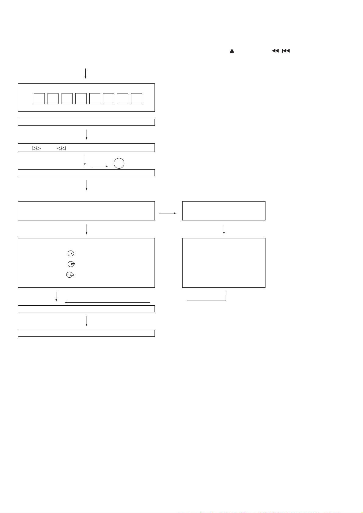
[2] Test mode
• Setting the test mode
During stand-by mode, press GAME/VIDEO button while pressing down the button and button. then,
press the CD button to enter the test mode.
C D T E S T
OPEN/CLOSE operation is using manual. IL isn’t done
<< >>,<< >>buttons make pick's slide possible.
to page 2-3
<<PLAY>> key input.
Do TOC IL. Do normal play.
When these following key is input into PLAY key, track number can be appoint directly.
<< 1>> key: Track 4
<< 2>> key: Track 9
<< 3>> key: Track 15
A
IL isn’t done
IL isn’t done
<<MEMORY>>
key input.
Adjustment result automatically will
display as below for each 2 sec:
a) "FOF_XXXX"
b) "TOF_XXXX"
c) "TBAL_XX"
d) "TGAN_XX"
f) "FGAN_XX"
g) "RFLS_XX"
<<STOP>> key input.
STOP
explanation:
a) Focus off set = "FOF_XXXX"
b)Tracking off set = "TOF_XXXX"
c)Tracking balance = "TBAL_XX"
d)Tracking Gain = "TGAN_XX"
f) Focus Gain = "FGAN_XX"
g) RF level shift = "RFLS_XX"
VOL — Last memory
P.GEQ — FLAT
X-BASS — OFF
To cancel : Power OFF
––––––––
2 – 2
Page 9
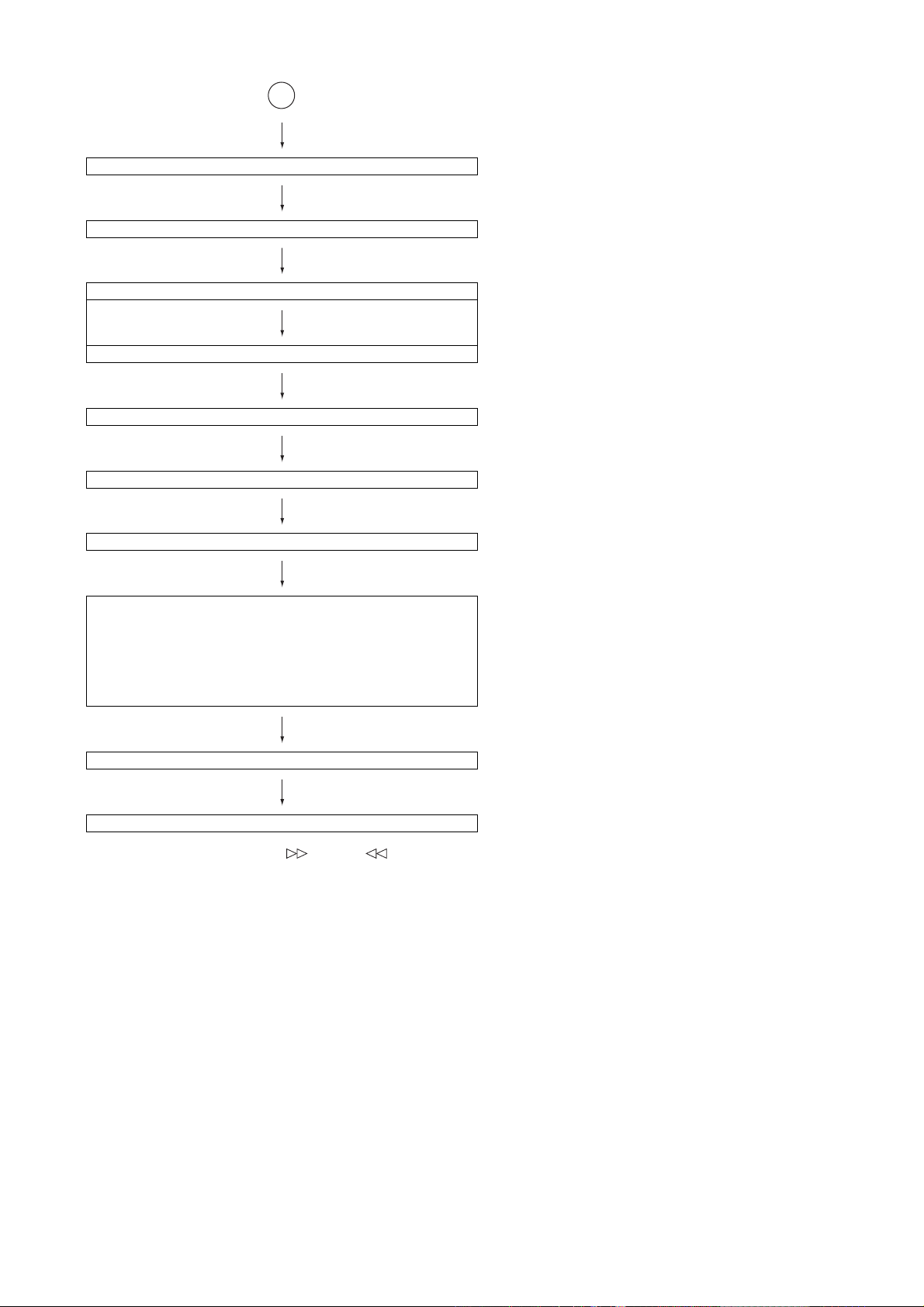
A
<<MEMORY>> key input.
Laser ON.
<<MEMORY>> key input.
Tracking OFF play at that specific point.
<<MEMORY>> key input.
Tracking ON play from that specific point.
CD-G15000/CP-G15000S
<<MEMORY>> key input.
Adjustment result automatically will display as below for each 2 sec :
a) "FOF_XXXX"
b) "TOF_XXXX"
c) "TBAL_XX"
d) "TGAN_XX"
f) "FGAN_XX"
g) "RFLS_XX"
<<STOP>> key input.
STOP
Sliding the PICKUP with<< >>, << >> button
must only be in STOP mode.
explanation:
a) Focus off set = "FOF_XXXX"
b)Tracking off set = "TOF_XXXX"
c)Tracking balance = "TBAL_XX"
d)Tracking Gain = "TGAN_XX"
f) Focus Gain = "FGAN_XX"
g) RF level shift = "RFLS_XX"
VOL — Last memory
P.GEQ — FLAT
X-BASS — OFF
To cancel : Power OFF
2 – 3
Page 10
CD-G15000/CP-G15000S
[3] CD section
CD Error code description
Error Explanation
10* CAM error. Can't detect CAM switch when CAM is moving.
11* When it detect cam operation error during initialize pro-
cess.
20* TRAY error. Can't detect TRAY switch when TRAY is mov-
ing.
21* When it detect TRAY operation error during initialize pro-
cess.
31 When it change to CD function, DSP cannot read initial
data.
* 'CHECKING'
If Error is detected, 'CHECKING' will be displayed
instead of 'ER-CD**'. 'ER-CD**' display will only be
displayed when error had been detected for the 5
times.
Standard Specification of Stereo System Error Message Display Contents
Error Contents Display Notes
CD CD Changer Mechanism Error. 'ER-CD**' (*) 10: CAM SW Detection NG during normal operation
CD DSP Communication Error. 'ER-CD31' DSP COMMUNICATION ERROR.
Focus Not Match/IL Time Over. 'NO DISC'
TUNER PLL Unlock. PLL Unlock.
th
11: CAM SW Detection NG during initialize process
20:TRAY SW Detection NG during normal operation
21:TRAY SW Detection NG during initialize process
(*) CHECKING:
If CD changer mechanism error is detected, 'CHECKING' will be display instead of 'ER-CD**'. 'ER-CD**'
display will only be display when error had been
detected for the 5
th
times.
Speaker abnormal detection and +B PROTECTION
display
In case speaker abnormal detection or +B PROTECTION had occurred, the unit will automatically enter to
stand - by mode and Timer indicator will be flashing as
below.
Example : In case of speaker abnormal
TIMER
LED
ON
OFF
NO. 1
NO.1 : +B Protection
NO.2 : Speaker abnormal
OFF
FLASHING
NO. 2
1 FRAME
OFF
NO. 1
+B PROTECTION is condition when irregular process
occur on power supply line.
BEFORE TRANSPORTING THE UNIT
The following process need to be taken after set taper-
ing/parts replacement.
ON
3. Press button until "WAIT"→ "FINISHED"
appears.
4. Unplug the AC cord and the unit is ready for transporting.
FLASHING
OFF
NO. 2
(REPEAT)
1. Press the ON/STAND-BY button to enter stand-by
mode.
2. While pressing down the button and the
button, press the GAME/VIDEO button. The Micro
Computer version number will be displayed as
"CM*****".
2 – 4
Page 11
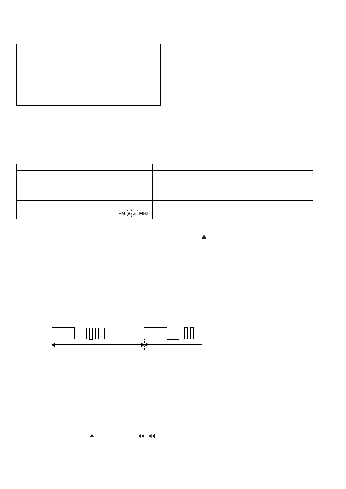
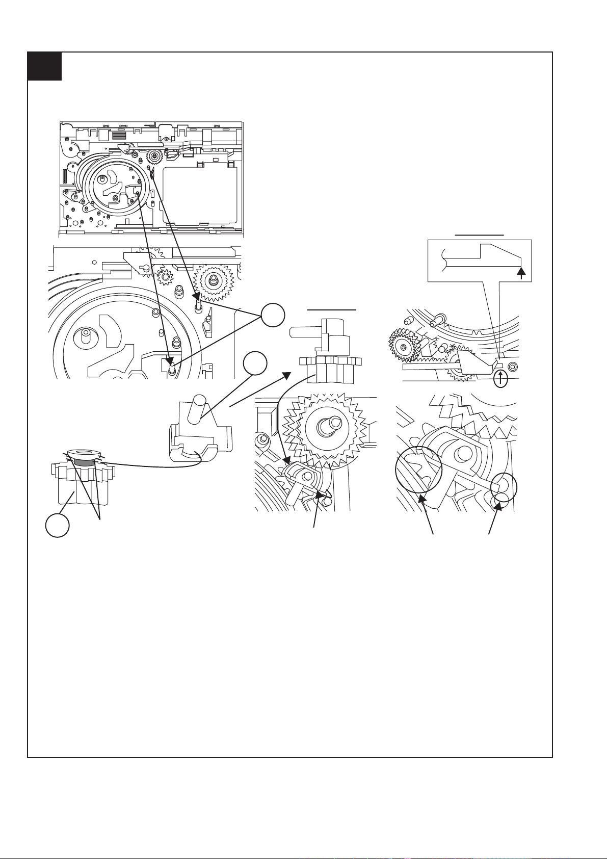
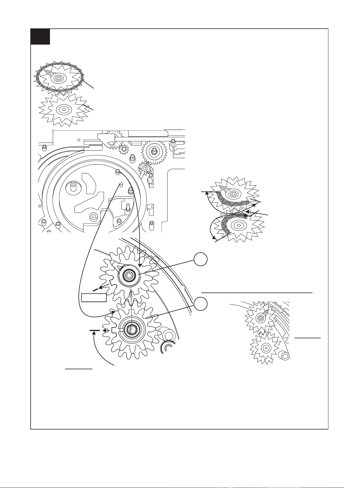
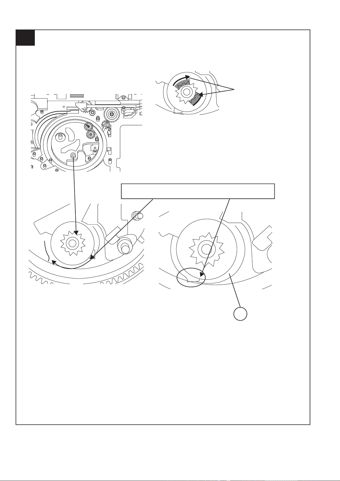
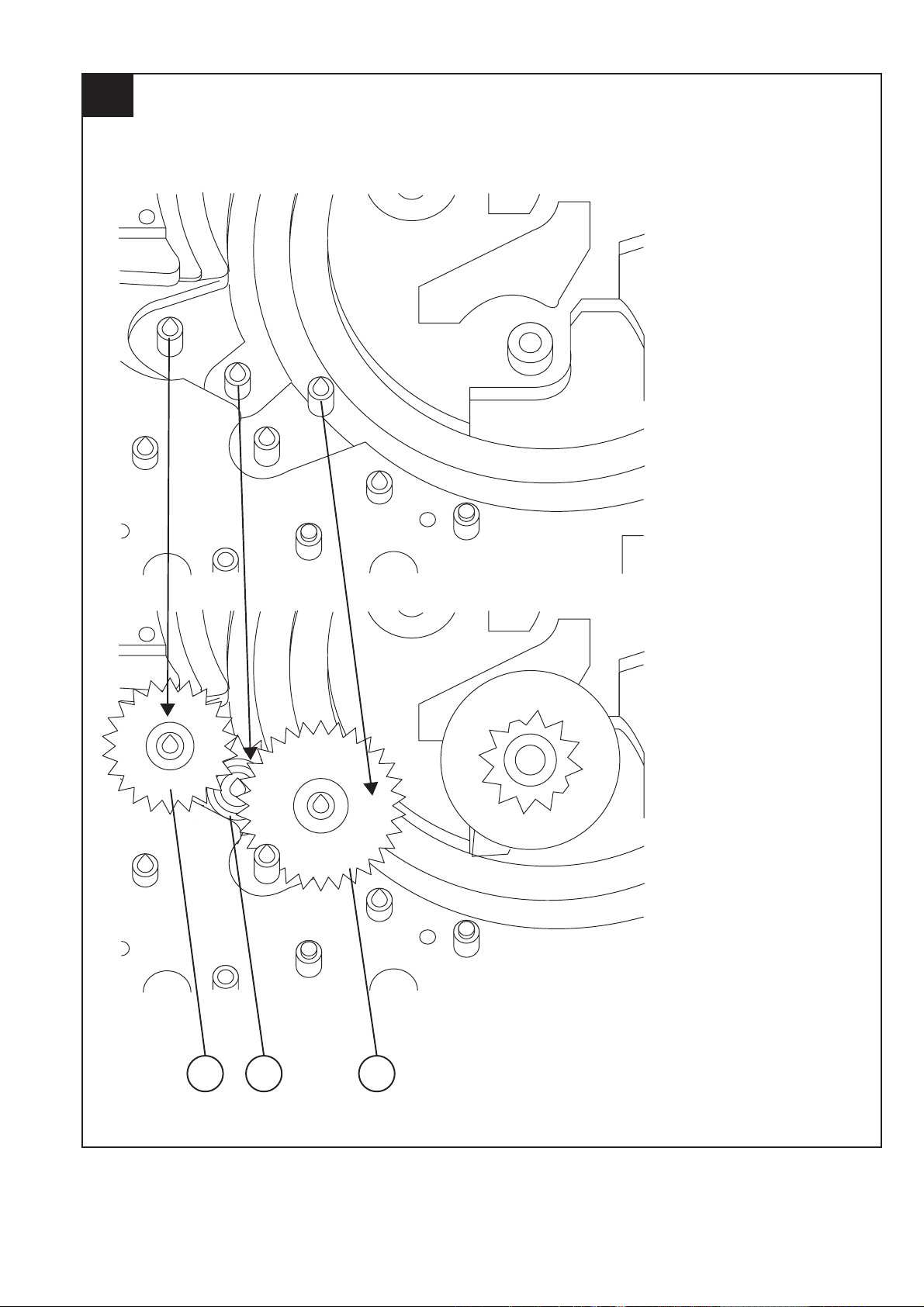
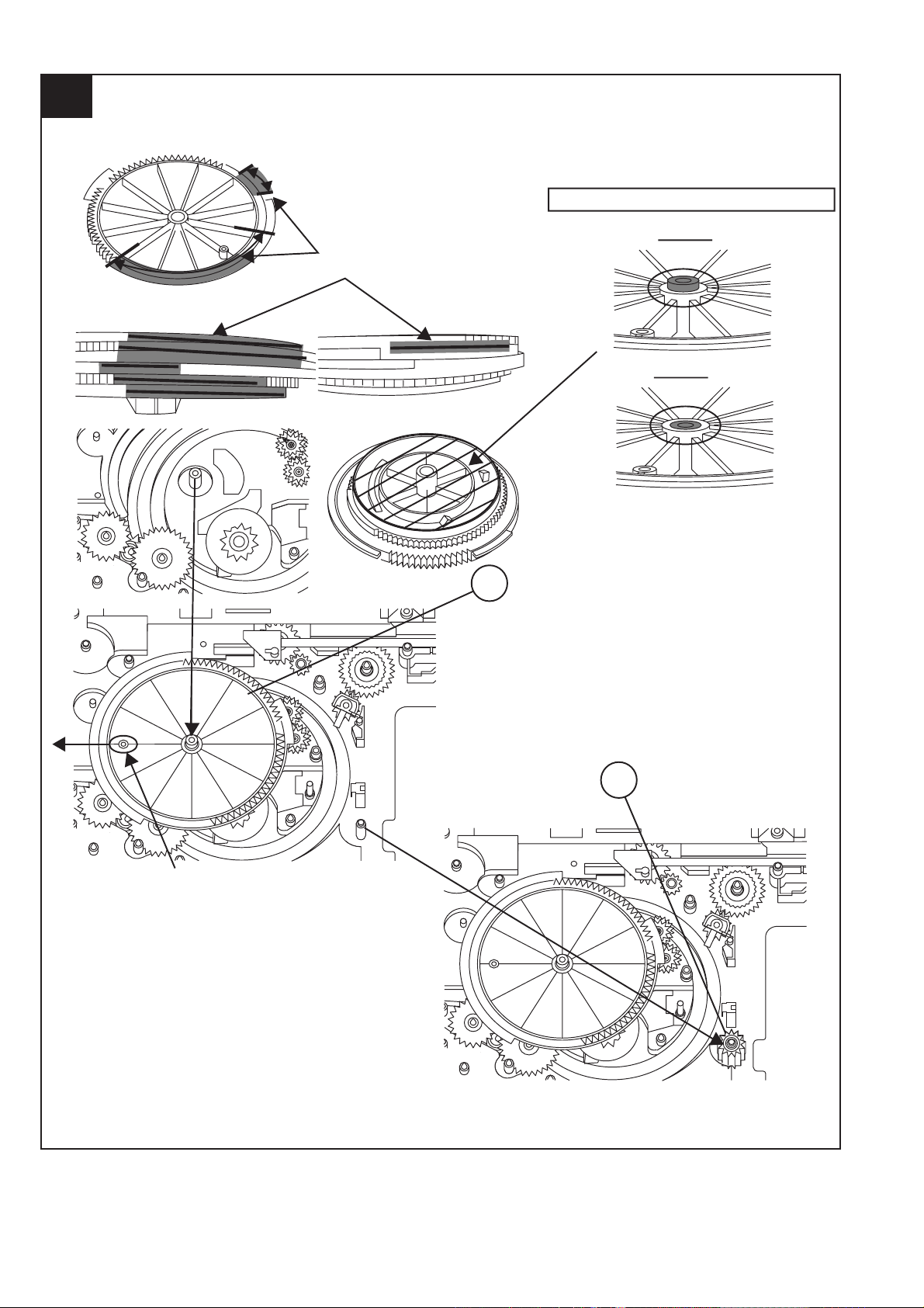
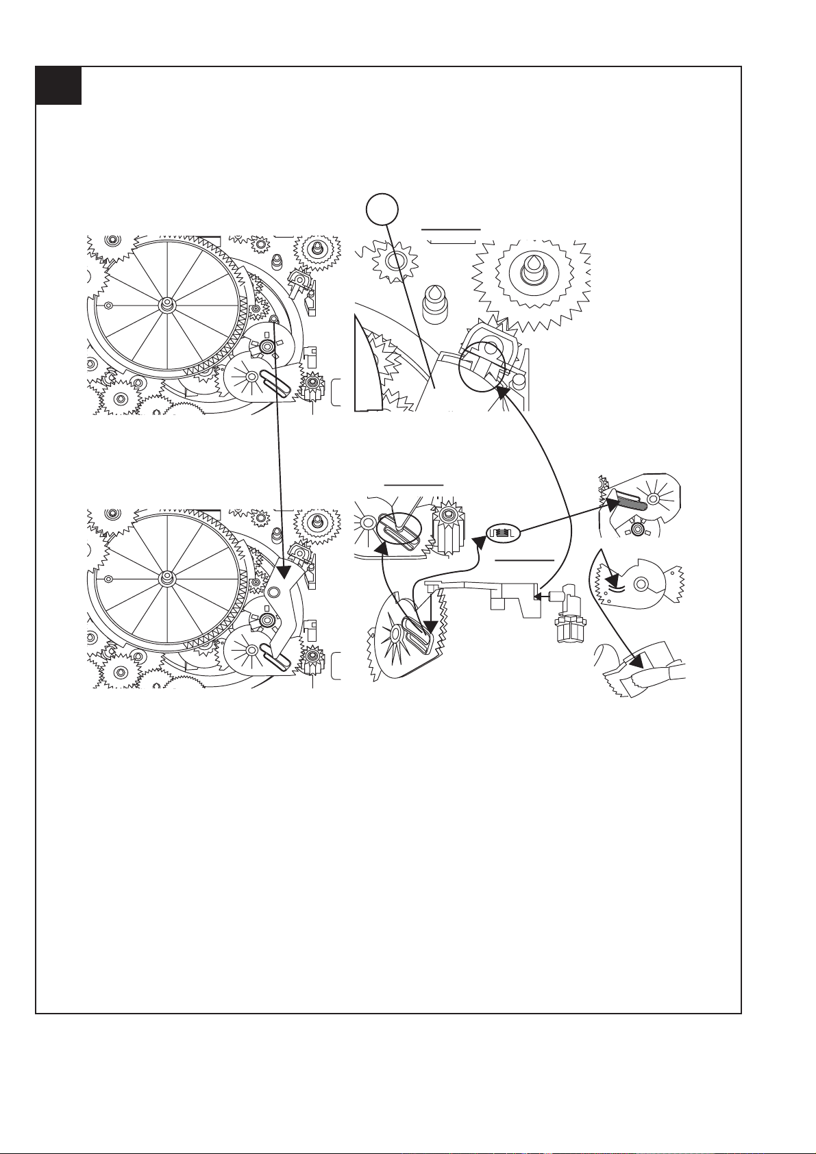
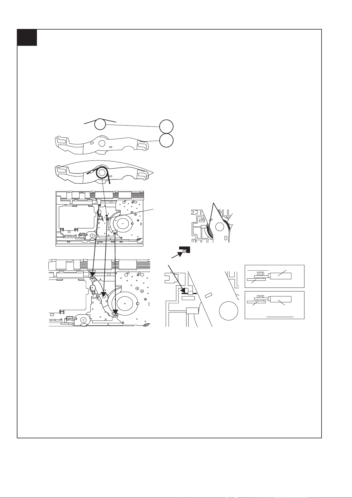
[4] CD Changer mechanism section
• All numbers in the drawing correspond to those in
parts guide (CHANGER MECHANISM PARTS).
1
CD-G15000/CP-G15000S
141
2 – 5
140
HALF GEAR
MUST BE ARRANGED AS SHOWN
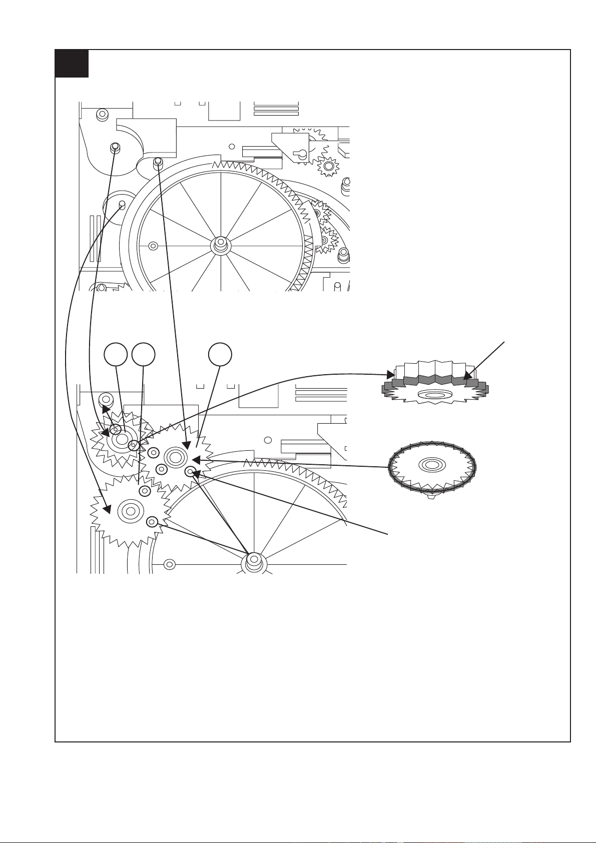
Page 12
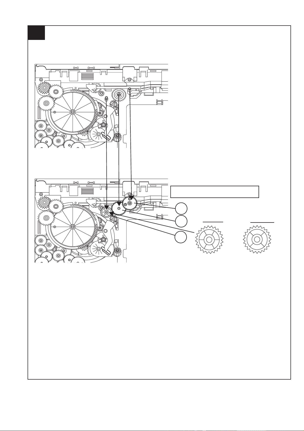
CD-G15000/CP-G15000S
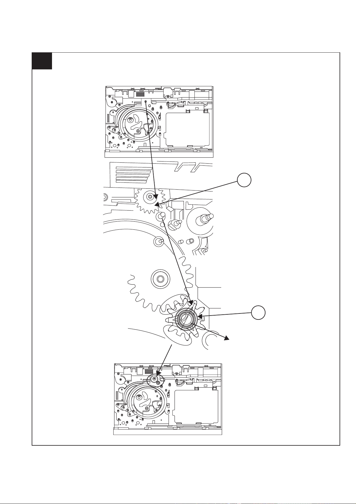
2
APPLY SANKOL SHS1001 BEFORE FIX
139
FIX ITEM 139 ACCORDING TO THE
PICTURE AS SHOWN ABOVE
ROTATE MODE BIG GEAR UNTIL REACH AS SHOWN IN PICTURE
2 – 6
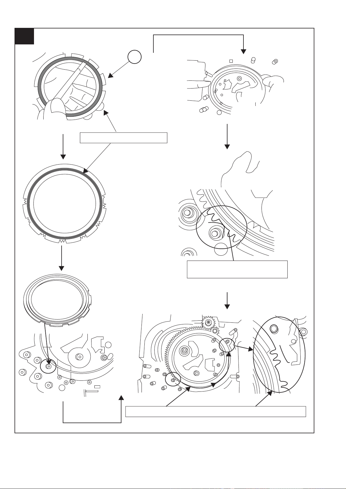
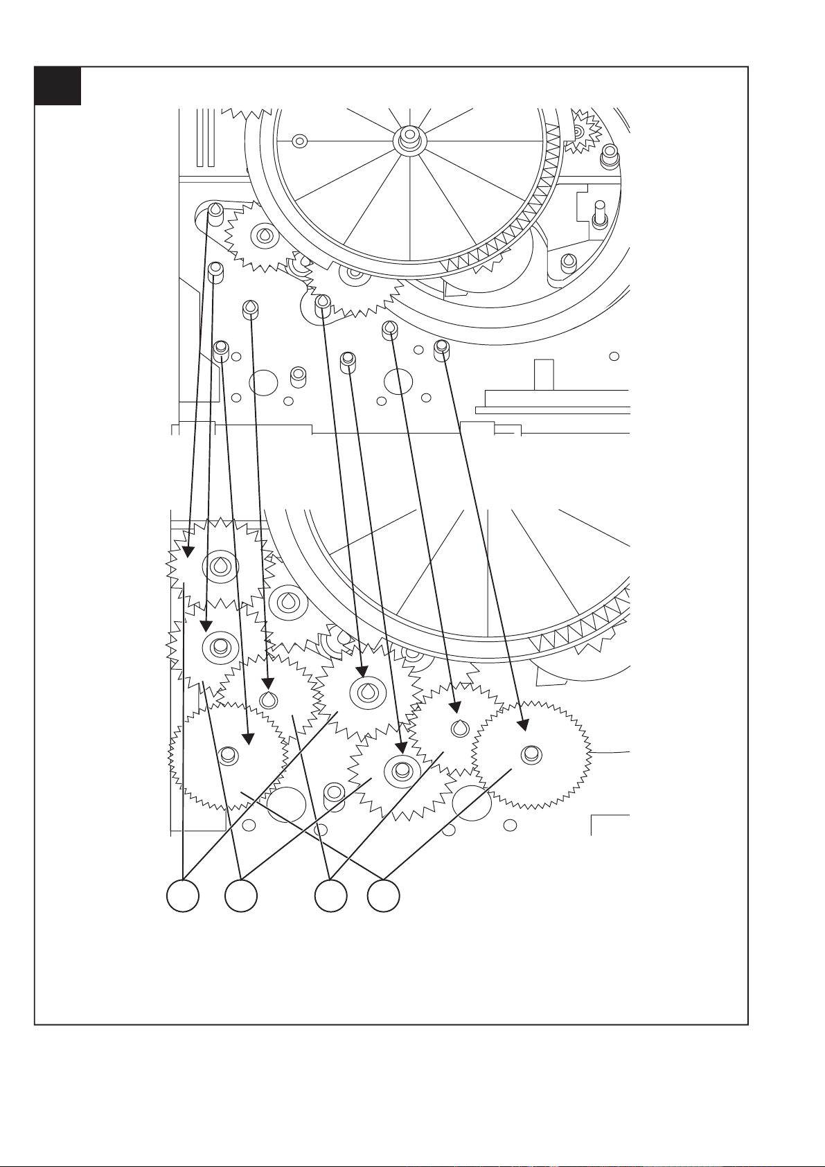
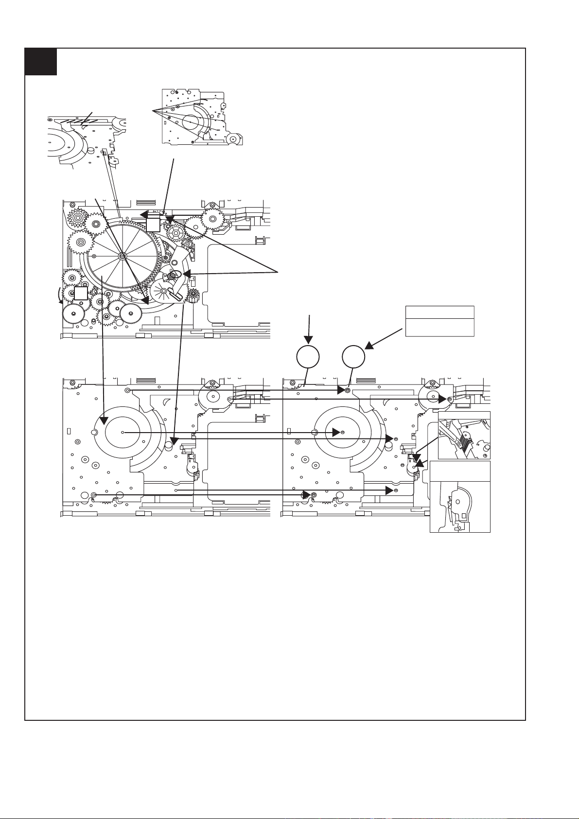
Page 13
APPLY GREASE SC141
PULL THE LEVER UNITIL
REACH THE ARROW MARK
143
112
3
CD-G15000/CP-G15000S
2 – 7
Page 14
CD-G15000/CP-G15000S
4
FIGURE 2
FIGURE 1
152
142
APPLY GREASE SC141
118
SLOT CLAMP
SWITCH ARM INSIDE BASE SLOT
HALF GEAR MUST BE
ARRANGED AS SHOWN
2 – 8
Page 15
5
CD-G15000/CP-G15000S
APPLY GREASE SC141 AT BOTTOM SIDE
OF GEAR FOLLOW MARKING (REFER TO GRAY AREA)
NO NEED TO APPLY GREASE AT BOTTOM
SIDE
FIGURE 1
APPLY GREASE SC141
AT TOP SIDE OF GEAR
FOLLOW MARKING
(REFER TO GRAY AREA)
127
IF DIRECTION IS OTHER THAN DIRECTION
SHOWN IN FIGURE 1, IT IS INCORRECT
CORRECT
128
INCORRECT
BLACK MARK
2 – 9
Page 16
CD-G15000/CP-G15000S
6
APPLY GREASE SC141 AT
HALF GEAR AREA
ROTATE CLOCKWISE UNTIL REACH HERE (MAXIMUM)
129
2 – 10
Page 17
7
CD-G15000/CP-G15000S
151150149
2 – 11
Page 18
CD-G15000/CP-G15000S
8
THE SHOW N AREA MUST FREE FROM GREASE
CORRECT
GREASE SC141 APPLICATION LENGTH
GREASE APPLICATION PORTION
INCORRECT
SHOWN HOLE MUST FACING ARROW DIRECTION
124
131
2 – 12
Page 19
9
138 126 125
CD-G15000/CP-G15000S
APPLY GREASE SC141
AT BOTTOM SIDE
ONLY
TR-RE JOINT GEAR C
APPLY GREASE SC141 ONLY AT TOP SIDE GEAR
MUST BE FIXED ACCORDINGLY TO
THE HOLE'S
2 – 13
Page 20
CD-G15000/CP-G15000S
10
148 147 146 145
2 – 14
Page 21
11
CD-G15000/CP-G15000S
121
144
WHEN FIXING ITEM 144 MUST FOLLOW AS SHOWN
APPLY GREASE SC141
130
2 – 15
Page 22
CD-G15000/CP-G15000S
12
117
FIGURE 2
FIGURE 1
APPLY GREASE
SC141
FIGURE 3
APPLY GREASE SC141
2 – 16
Page 23
13
CD-G15000/CP-G15000S
ITEM 133 , 134 MUST APPLY GREASE SC141
ON TOP SIDE GEAR ONLY
134
GEAR 112 GEAR 112
133
132
CORRECT
TOP VIEW AFTER
BEING ASSEMBLED
INCORRECT
IT IS INCORRECT TO
FIX IT IN REVERSED
DIRECTION
2 – 17
Page 24
CD-G15000/CP-G15000S
14
APPLY GREASE SC141
BEFORE FIX
MOVE 112 UNTIL TOUCH THE WALL
A
B
DURING GEAR A ROTATE
MUST PRESS SHOWN AREA
AND LEVER B WILL MOVE
ARROW DIRECTION THEN
FIX PART 108
SCREW TORQUE
+0.5
2 kgf-cm
-0
108 803 x6
APPLY GREASE SC141
CONFIRM WHETHER
FIXED
PROPELY OR NOT
2 – 18
Page 25
15
CD-G15000/CP-G15000S
APPLY GREASE SC141
113
BEHIND THE LEVER NEED TO APPLY GREASE SC141
PULL IT THEN LEVER WILL
MOVE IN
2 – 19
Page 26
CD-G15000/CP-G15000S
16
123
115
APPLY GREASE SC141
APPLY GREASE SC141 BEFORE FIX
APPLY GREASE
SC141 AT BOSS
SPRING MUST BE ARRANGED UNDER THE HOOK
CORRECT LR JOINT LEV
BOARD R
BOARD R
LR JOINT LEV
INCORRECT
2 – 20
Page 27
17
CD-G15000/CP-G15000S
IT IS INCORRECT IF ASSEMBLED IN
REVERSED DIRECTION
103 137 136
APPLY GREASE SC141
BIG SLOT MUST FACING OUT
WHEN FIX AND AFTER FIXED TO BASE CHASSIS.
AFTER ASSEMBLY, CONFIRM WITH FREE DROP TEST
GEAR POSITION DURING FIXING
2 – 21
Page 28
CD-G15000/CP-G15000S
18
IT IS INCORRECT IF ASSEMBLED IN
REVERSED DIRECTION
APPLY GREASE SC141
104
135
136
BIG SLOT MUST FACING OUT
WHEN FIX AND AFTER FIXED TO BASE CHASSIS
AFTER ASSEMBLY, CONFIRM WITH FREE DROP TEST
GEAR POSITION DURING FIXING
CONFIRM BOTH GEARS SIT PROPERLY AND LOCKED
2 – 22
Page 29
AFTER FIX OUTER UP/DOWN LEVER HOLD AS SHOWN PORTION AND
MOVE UP/DOWN THEN CONFIRM WHETHER LEVER GO INSIDE THE HOLE OR NOT
IT IS INCORRECT IF THE LEVER HOLD DOES NOT
ENTER THE HOLE
IT IS CORRECT IF THE LEVER HOLD
ENTERS THE HOLE
19
ALL OF THIS 135 AND 137 GEAR FIX TOGETHER WITH 119
AND 120 LEVER ( MOVE TOGETHER )
BIGGER SLOT FACING OUT
119
135
BIGGER SLOT FACING OUT
120
137
CD-G15000/CP-G15000S
2 – 23
Page 30
CD-G15000/CP-G15000S
20
BIGSLOTFACINGOUT
110
2 – 24
Page 31

21
CD-G15000/CP-G15000S
PUSH THE LEVER ACCORDING TO ARROW
DIRECTION THEN FIX
WHEN FIXING MAIN BASE ASSEMBLY FOLLOW ACCORDING TO PICTURE 1
PICTURE 1
CORRECT INCORRECT INCORRECT
MAKE SURE MECHA HOLDER SHAFT FIX PROPERLY TO LEVER
PICTURE 3
PICTURE 2
2 – 25
Page 32

CD-G15000/CP-G15000S
22
APPLY SANKOL (SHS1001)
101
102
APPLY SANKOL
(SHS1001) ON TOP
APPLY SANKOL (SHS1001) INSIDE
THE SLOT & OTHER SHOWN PORTION
APPLY SANKOL
(SHS1001)
APPLY SANKOL (SHS1001) AT
TRAY SLIDING PORTION
FIX TRAY NO 1 FIRST THAN
FOLLOW OTHER
APPLY SANKOL (SHS1001) AT BACK PORTION
COSMO GUIDE TRAY HAVE
MARKING AS SHOWN
2 – 26
Page 33

AFTER ASSEMBLY GEAR UP/DOWN BOARD
APPLY GREASE SC141 AT INNER & OUTER GEAR SLIDING PORTION
WHEN FIX GEAR UP/
DOWN BOARD THE
TWO LEVER MUST AT
PARALLEL LINE AND
POSITIONED AT TOP
MAX SIDE
111
23
GEAR UP/DOW N BOARD
CD-G15000/CP-G15000S
2 – 27
Page 34

CD-G15000/CP-G15000S
24
SCREW TORQUE
+0.5
3 kgf-cm
-0
ROTATE THE GEAR TO MOVE UP 111 GEAR
UP AND DOWN BOARD BEFORE SCREW
804
2 – 28
Page 35

25
CD-G15000/CP-G15000S
AFTER ASSEMBLY TOP PLATE
FIX THE FFC
FFC4
AFTER PUSH, MAKE SURE SNAP PROPERLY
AFTER FIX, PUSH FOLLOW ARROW DIRECTION
BEFORE LOCK
AFTER LOCK
BACK
PORTION
107
122
BEFORE LOCK
PRESS IN
SLOT IN
BEFORE LOCK
AFTER LOCK
AFTER LOCK
MUST CONFIRM
MUST CONFIRM
2 – 29
Page 36

CD-G15000/CP-G15000S
26
CORRECT
INCORRECT
CAUTION
1. MAKE SURE NO PWB CHIP INSIDE SET .( BEFORE FIX MAKE
SURE PW B IS FREE FROM DUST , GREASE & ETC )
803
2 – 30
Page 37

27
THE TW O SLOT MUST FREE
FROM GREASE SC141
APPLY GREASE SC141
BELOW THE MARKING
FOR BOTH PORTION
CD-G15000/CP-G15000S
ASSEMBLY SEQUENCE
1. APPLY GREASE SC141 TO MAIN BASE
GREASE SC141 APPLICATION AREA
ALL BOSS
APPLY GREASE SC141
APPLY GREASE
SC141
CAUTION
TRAY SLIDING
AREA MUST
FREE FROM
GREASE SC141
APPLY GREASE
SC141
APPLY GREASE
APPLY GREASE SC141 AT WALL
APPLY GREASE
SC141
SC141
105
APPLY GREASE SC141
AT BOTH SLOT
APPLY GREASE SC141 AT 3 HALF MOON
1 RIB ONLY
APPLY GREASE
SC141
APPLY GREASE SC141
INSIDE SLOT
2 – 31
Page 38

CD-G15000/CP-G15000S
28
REFERENCE ONLY
MOTOR GEAR HEIGHT FROM
MAIN BASE 12.2
+
0.1
-
0.1
-
+
12.2
MOTOR SCREWING HOLE
MUST HAVE GAP
M1,2
801
-0
13.8 + 0.2
APPLY GREASE SC141
SCREW TORQUE
1.5 + 0.5
-0
AFTER SCREW MOTOR, CONFIRM THE
ARRANGEMENT AS IN FIGURE 2
FIGURE 2
2 – 32
Page 39

29
APPLY SANKOL (SHS1001)
CD-G15000/CP-G15000S
3.1 + 0.1
SHAFT X 3 DIM AFTER INSERTION
MUST CONFIRM EVERYDAY
109-2
APPLY GREASE AT THE SLIDING PORTION
114
116
UP / DOWN
HOLDER CHANGE
TO NATURE
COLOR
SANKOL
APPLICATION AREA
(SHS1001)
APPLY GREASE SC141
2 – 33
Page 40

CD-G15000/CP-G15000S
30
BEFORE MELT IT
AFTER MELT IT ( MUST FLAT )
CHANGE COLOR
TO NATURE
WHEN FITTING STABILIZER PLATE TO STABILIZER,
ROTATE STABILIZER ANTI CLOCKW ISE BY JIG
( ! STRICLY CANNOT FIT USING HAND )
AFTER ASSEMBLED TO
HOLDER, STABILIZER
NEED TO BE CLEANED
WITH ALCOHOL DISC
TOUCHING SURFACE
BELOW
2 – 34
Page 41

31
CD-G15000/CP-G15000S
106
APPLY GREASE SC141
MUST MAKE SURE SNAP PROPERLY BOTH SIDE
ALL SURFACE MUST TOUCH
CORRECT INCORRECT
GAP
INCORRECT
2 – 35
Page 42

CD-G15000/CP-G15000S
32
NO GAP HAVE GAP
CORRECT INCORRECT
2 – 36
Page 43

Note:
After removing the connector for the optical pickup from the
connector, wrap the conductive aluminium foil around the front end
of the connector so as to protect the optical pickup from electrostatic damage.
Figure 2
Figure 1
Figure 3
(C1)x1
PULL
PULL
Lug wire
(E1)x1
3x10mm
Fan Motor
Rear Panel
(C1)x1
Hook
Hook
3x10mm
(D1)x9
3x10mm
(E2)x1
(E3)x1
Power PWB
Main PWB
Front Panel
(F1)x1
O
O
O
(C2) x1
(C3) x1
CD Changer
Unit
CD Servo PWB
(A1)x1
3x12mm
Rear Panel
3x12mm
(Left)
(B1)x2
3x10mm
(B1)x2
3x10mm
(B1)x2
3x10mm
(B1)x2
3x10mm
Side Panel
(Right)
(A1)x2
3x12mm
Side Panel
(A1)x2
Front Panel
Top Cabinet
STEP REMOVAL PROCEDURE FIGURE
1
Top Cabinet
1. Screw…………..……….(A1) X 5 1
2
Side Panel (Left/
2. Screw……….…………..(B1) X 8
1
Right)
3 CD Changer unit 1. Hook ……………………(C1) X 2 2
2. Socket………………..…(C2) X 1
3. Flat Cable ……… …….(C3) X 1
4 Rear Panel with
1. Screw………..………….(D1) X 9 2
Fan motor
5 Front Panel
1. Screw………………..….(E1) X 3 2,3
2. Flat Cable ………..…….(E2) X 1 2
3. Socket……..……………(E3) X 1 2
4. Hook …………….…...…(E4) X 2 3
6 Main PWB 1. Screw………………..….(F1) X 5
2,3
2. Socket……..……………(F2) X 4 3
3. Flat Cable ……………...(F3) X 1
3
7 Power PWB 1. Screw………………..….(G1) X 4 3
8 Tape Mechanism 1. Screw…….…………..….(H1) X 6 4
2. Flat Cable ………..…….(H2) X 1
9 Game Input PWB 1. Screw………………..….(J1) X 2 5
10 Display PW B 1. Knob……..…………..….(K1) X 1
2. Nut……………..……..….(K2) X 1 5
3. W asher……..….………..(K3) X 1
4. Screw……..……………..(K4) X 6
11 Speaker PWB 1. Screw………………..….(L1) X 3 6
12 CD Servo PWB
1. Screw…….………….….(M1) X 3
7
2. Flat Cable ………..…….(M2) X 2
3. Socket……..……………(M3) X 1
13
Changer 1. Screw…….………….….(N1) X 4 8
Mechanism Unit
2. Changer Chassis………(N2) X 1
14 CD Mechanism 1. Screw…….………….….(P1) X 4 9
PULL
PULL
Hoo k
(E4)x1
4x8mm
(G1)x4
Power PWB
(F2)x1
(F2)x2
(F3)x1
Front Panel
(F2)x1
3x8mm
(E1)x2
3x6mm
(F1)x4
(E4)x1
CD-G15000/CP-G15000S
CD-ES700/CD-ES77CD-ES700/CD-ES77Service ManualCD-ES700/CD-ES77MarketE
CHAPTER 3. MECHANISM BLOCKS
CHAPTER 3.
[1] Caution on disassembly
Caution on Disassembly
Follow the below-mentioned notes when disassembling the unit and reassembling it, to keep it safe and ensure
excellent performance:
1. Take cassette tape and compact disc out of the unit.
2. Be sure to remove the power supply plug from the wall outlet before starting to disassemble the unit.
3. Take off nylon bands or wire holders where they need to b e remove d when disassemb ling the unit. After servicing
the unit, be sure to rearrange the leads where they were before disassembling.
3 – 1
Page 44

CD-G15000/CP-G15000S
O
(H1)x6
3x10mm
Figure 4
Tape
Mechanism
(K4)x6
2.6x10mm
(H2)x1
Lug wire
Front Panel
Front Panel
Display PWB
(K2)x1
(K1)x1
(K3)x1
(M2)x1
Figure 7
(M1)x3
3x10mm
(N1)x4
3x10mm
(M3)x1
CD Servo
PWB
(M2)x1
Changer
Mechanism
Unit
Figure 5
(J1)x2
Special
(L1)x3
Ø3x10mm
Figure 6
Game Input
PWB
Speaker PWB
Figure 8
(P1)x4
2.6x10mm
CD Mechanism
(N2)x1
Changer
Mechanism
Unit
Changer
Mechanism
Unit
3 – 2
Figure 9
Page 45

STEP
1 Woofer 1. Front Panel Ass'y…..(A1) X 1 10
Tweeter 1. Screw……...….....….(B1) X 2 12
2. Screw.…….……...…(A2) X 8 11
1 Woofer 1. Front Panel Ass'y…..(A1) X 1 13
2. Screw.…….……...…(A2) X 8 14
2
REMOVAL PROCEDURE FIGURE STEP REMOVAL PROCEDURE FIGURE
CP-G15000 GBOXSA133AWM1
(A1)x1
Speaker Box Assembly
Driver should
be pried away
from Speaker Box.
Figure 13
Screwdriver
Ø3.5x16mm
Ø3.5x16mm
(A2)x4
(A2)x4
Speaker Box Assembly
WOOFER
WOOFER
Figure 14
Figure 12
(A1)x1
Speaker Box Assembly
from Speaker Box.
be pried away
Driver should
Figure 10
Screwdriver
Ø4x16mm
Ø4x16mm
WOOFER
WOOFER
(A2)x4
(A2)x4
Speaker Box Assembly
Figure 11
Ø3x10mm
TWEETER
(B1)x2
Front Panel Assembly
CD-G15000/CP-G15000S
3 – 3
Page 46

CD-G15000/CP-G15000S
CP-SW15000
STEP PROCEDURE FIGURE
REMOVAL
Subwoofer Panel
1 1. Screw Cover……. ……..(A1) X 4 15
2. Catching Holder……..…(A2) X 4
3. Screw …………………..(A3) X 4
4. Socket ………………….(A4) X 1
2 1. Screw Cover……. ……..(B1) X 4 15
AMP Front Panel
2. Catching Holder……..…(B2) X 4
3. Screw …………………..(B3) X 4
4. Socket ………………….(B4) X 3
Rear Plate
3 1. Screw …………………..(C1) X 8 15
Subwoofer Speaker
4 1. Screw …………………..(D1) X 2 16
LED PWB
Power Switch PWB
5 1. Screw …………………..(E1) X 2 17
Volume PWB
6 1. Screw …………………..(F1) X 4 17
LED Flashing PW B
7 1. Screw …………………..(G1) X 2 17
Subwoofer
8 1. Screw …………………..(H1) X 8 18
AMP Chassis Assembly
9 1. Screw …………………...(J1) X 8 18
10 1. Screw …………………..(K1) X 2 19
Fan Assembly
11 1. Screw …………………...(L1) X 1 19
Jack PWB
12 Subwoofer AMP PWB 1. Screw …………………..(M1) X 9 20
13 1. Screw …………………..(N1) X 2 20
Primary Power PW B
(A1)x4
2. Screw …………………..(C2) X 1
2. Socket ………………….(G2) X 1
2. Screw …………………...(J2) X 2
3. Screw …………………...(J3) X 6
2. Socket …………….…….(K2) X 1
2. Socket …………….…….(L2) X 1
2. Socket …………….…….(M2) X 4
2. Socket ………………….(N2) X 3
(A2)x4
(A3)x4
M4x40mm
Subwoofer Panel
Figure 17
Subwoofer Panel
Figure 16
AMP Front Panel
Power switch PWB
(F1)x4
M3x10mm
Volume PWB
(G2)x1
LED Flashing PWB
(G1)x2
M3x10mm
Subwoofer speaker
LED PWB
(D1)x2
M2.6x8mm
(E1)x2
Washer Screw
(B1)x4
(B2)x4
(B3)x4
M4x40mm
AMP Front Panel
(B4)x3
Rear Plate
Figure 15
(A4)x1
Speaker Box Assembly
(C1)x8
M4x16mm
(C2)x1
M3x10mm
(H1)x8
M4x16mm
M4x16mm
(J1)x8
Subwoofer
(J2)x2
Washer Screw
Figure 18
Speaker Box Assembly
AMP Chassis
Assembly
(J3)x6
M4x16mm
3 – 4
Page 47

CD-G15000/CP-G15000S
(M2)x3
(M2)x1
AMP PWB
Subwoofer
(K1)x2
(K2)x1
Fan
Assembly
AMP Chassis
Assembly
Washer Screw
(L2)x1
M3x8mm
(L1)x1
Jack PWB
Figure 19
Figure 20
(M1)x9
M3x8mm
M3x8mm
Primary
Power PWB
(N2)x3
(N1)x2
3 – 5
Page 48

CD-G15000/CP-G15000S
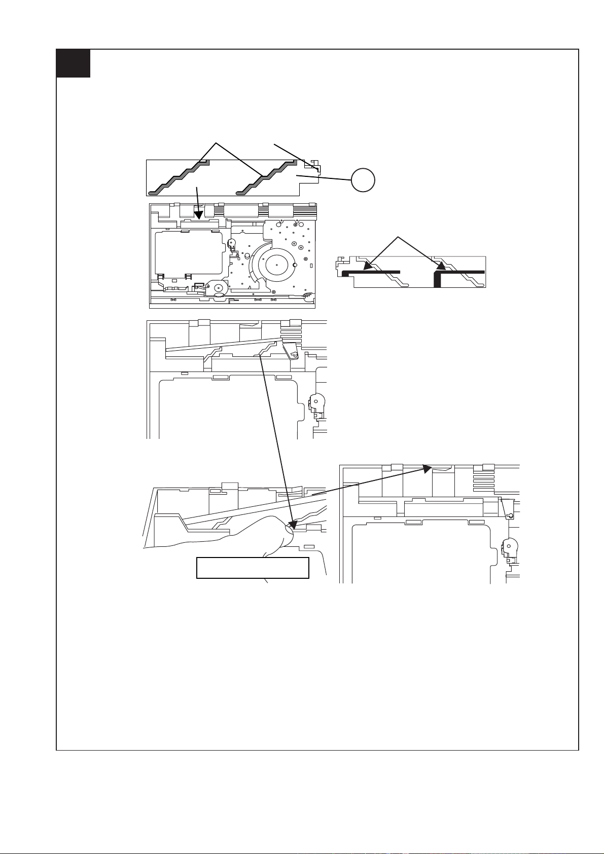
[2] Removing and reinstalling the main parts
1. TAPE MECHANISM SECTION
Perform steps 1 to 5 and 6 of the disassembly method
to remove the tape mechanism.
1.1. How to remove the record/playback and erase
heads (TAPE 2) (See Fig. 1)
1. When you remove the screws (A1) x 2 pcs., the
recording/playback head and three-dimensional
head of the erasing head can be removed.
Erase Head
(A1)x2
φ2x9mm
TAPE 2
Clutch Ass'y
Record/Playback
Head
Figure 1
1.2. How to remove the playback head (TAPE
1)(See Fig. 2)
1. When you remove the screws (B1) x 2 pcs., the
playback head can be removed.
TAPE 1
Clutch Ass'y
Playback
Head
Pinch
Pinch Roller
(C1)x1
Pull
<B>
<A>
Roller
Pawl
Figure 3
1.4. How to remove the belt (TAPE 2) (See Fig. 4)
1. Remove the main belt (D1) x 1 pc., from the motor
side.
2. Remove the FF/REW belt (D2) x 1 pc.
1.5. How to remove the belt (TAPE 1) (See Fig. 4)
1. Remove the main belt (E1) x 1 pc., from the motor
side.
2. Remove the FF/REW belt (E2) x 1 pc.
Tape
Motor
TAPE 2
Main Belt
(D1)x1
TAPE 1
Main Belt
(E1)x1
TAPE 1
FF/REW
Belt
(E2)x1
TAPE 2
FF/REW
Belt
(D2)x1
Main Belt
(D1)x1
Main Belt
(E1)x1
Tape
Motor
Figure 4
1.6. How to remove the motor (See Fig. 5)
1. Remove the screws (F1) x 2 pcs., to remove the
motor.
Tape
Motor
(B1)x2
φ2x9mm
Figure 2
1.3. How to remove the pinch roller (TAPE 1/2) (See
Fig. 3)
1. Carefully bend the pinch roller pawl in the direction
of the arrow <A>, and remove the pinch roller (C1) x
1 pc., in the direction of the arrow <B>.
Note:
When installing the pinch roller, pay attention to the
spring mounting position.
Clutch Ass'y
(F1)x2
φ2.6x5mm
Figure 5
2. CD MECHANISM SECTION
Perform steps 1, 2, 9, 10, 11 and 12 of the disassembly method to remove the CD mechanism.
3 – 6
Page 49

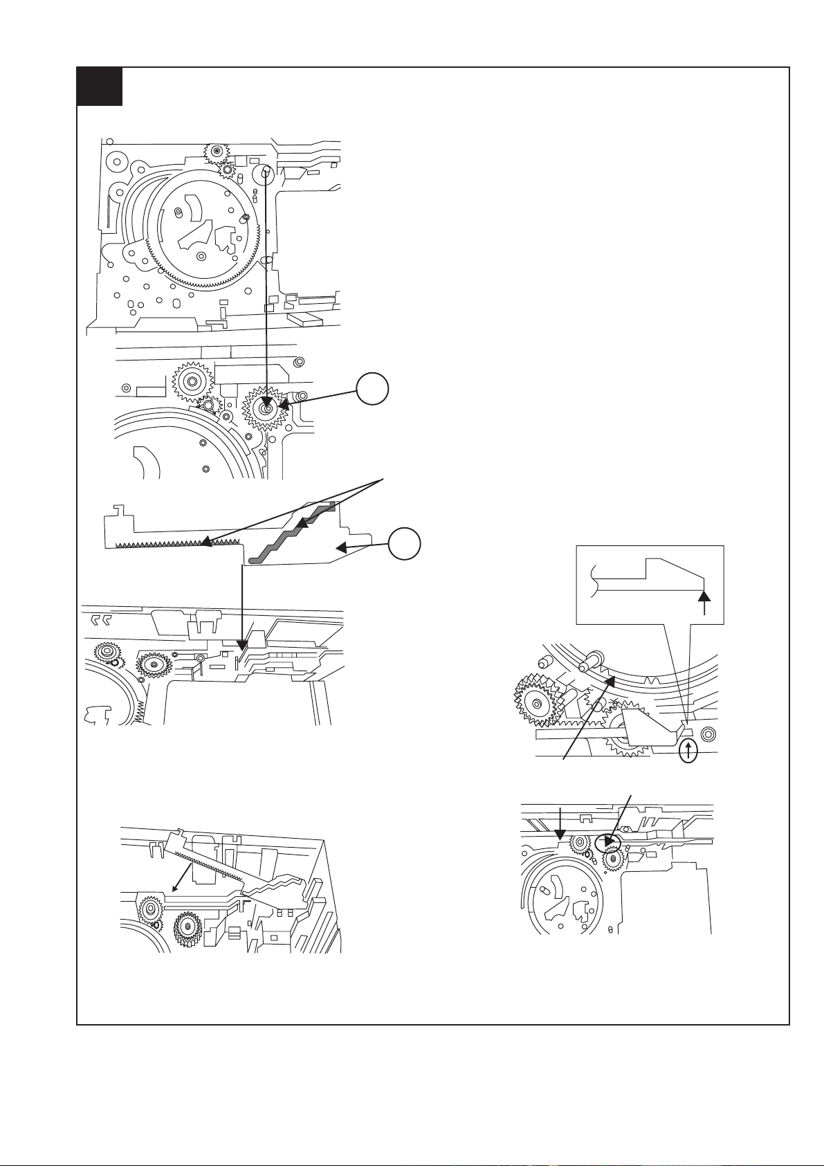
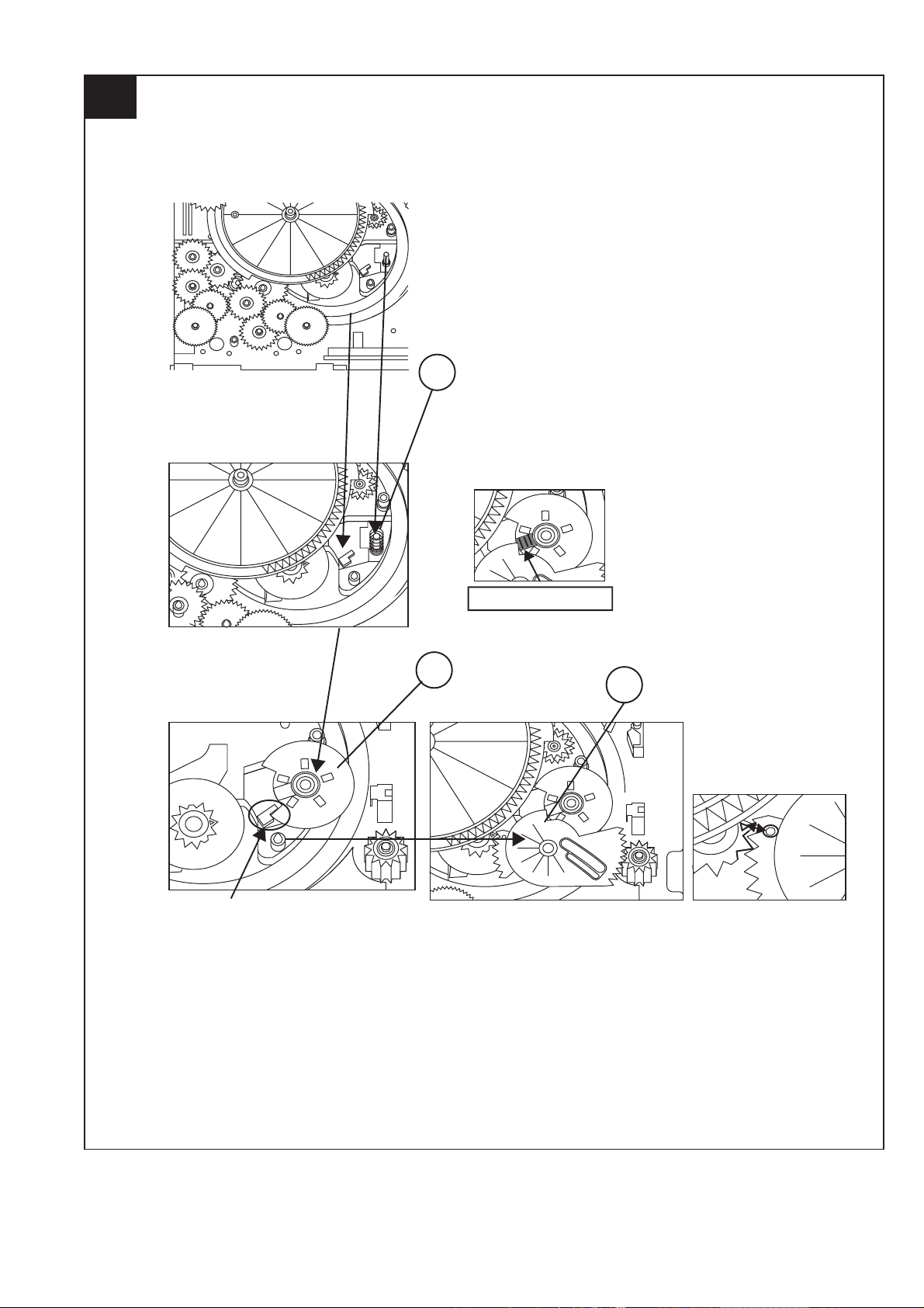
2.1. Remove the pickup. (See Fig. 1)
Mark 1
(DISC 1)
(DISC 2)
(DISC 3)
(DISC 4)
(DISC 5)
Gear up down board
Mark 3 Mark 5
Mark 2 Mark 4
1. Remove the stop washer (A1) x 1 pc., to remove the
gear (A2) x 1 pc.
2. Remove the screws (A3) x 2 pcs., to remove the
shaft (A4) x 1 pc.
3. Remove the pickup.
Note:
After removing the connector for the optical pickup
from the connector wrap the conductive aluminium foil
around the front end of connector so as to protect the
optical pickup from electrostatic damage.
(A3)x2
φ2.6x6mm
CD Mechanism
Shaft
(A4)x1
Gear
(A2)x1
Stop Washer
(A1)x1
CD-G15000/CP-G15000S
Reduction gear C
Front Rear
Figure 3
2. In another case, if CD mechanism is at tray No.1
play position and to remove CD located in tr ay No.3,
the procedure is as follows:
If the gear up down board is located at tray No.1
position, then rotate gear clock-wise until it at stock
position. Rotate reduction gear D clockwise (Figure
4) to move the CD mechanism to tray No.3 position.This is confirmed by checking the gear up down
board position by the marking as indicated on the
main chassis as shown in Figure 5.
Reduction gear D
Pickup Unit
Figure 1
3. CHANGER MECHANISM SECTION
Perform steps 1, 2, 9 and 10 of the disassembly
method to remove the CD changer mechanism.
3.1. How to remove CD Disc (See Fig. 2~5)
1. When CD is at play position (Figure 2), rotate r eduction gear C clock-wise as shown in Figure 3 Until
disc tray is at stock position, then rotate further to
eject the disc tray so that CD can be removed from
the tray.
CD Disc
Disc Tray
Guide Tray
CD At play position.
CD Disc
Up Down
Figure 4
Figure 5
CD At stalk position.
Figure 2
3 – 7
Page 50

CD-G15000/CP-G15000S
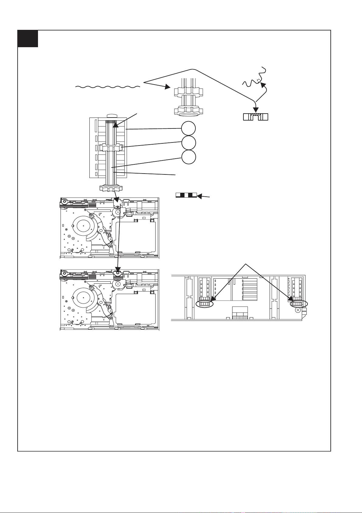
3.2. How to Remove the tray motor/main cam
motor/5-Changer Motor PWB (See Fig. 1)
1. Remove the screws (A1)x 2 pcs., to remove tray
motor/main cam motor/5-Changer Motor PWB.
Changer Mechanism Unit
Main Cam Motor
(A1)X2
φ2x10mm
Figure 1
Tray Motor
5-Changer
Motor PWB
NOTE:There are 2 more screws tighten the motors at
the bottom of main chassis. Before performing
procedure 1 above, disc stop spring, top plate
sear up down board and trays must be
removed, then only the 2 screws can be
untighten.
3 – 8
Page 51

CHAPTER 4. DIAGRAMS
CHAPTER 4. DIAGRAMS
[1] CD Block diagrams
CD-G15000/CP-G15000S
XL1
16.9344 MHz
+3.3V
CONSTANT
VOLTAGE
TO MAIN SECTION
R-CH
AGND
L-CH
CE
43
CL
44
DI
45
DO
46
RESB
47
INTB0
48
INTB1
49
XOUT
72
XIN
73
DVDD
AVDD
36 41
+3.3V
D_+5V(+B5)
DGND
7875
LCHO
+8V(+B7)
MGND
7123 456
CNP3
RCHO
LC78690E
CD SERVO
XVDD
74
LRVDD
76 876521
IC1
Q1
TO DISPLAY SECTION
+B6
GND
PHOTO
MO_A-
BIN
CIN
AIN
LASER
DRIVER
MO_A+
DIN
EIN
CD_RESB
CD_DI
CD_CLK
5251
CONT1
CONT0
FIN
1413
CD_DO
10
SLDO
SPDO
LDS
181968
CD_CE
PUIN
FDO
TDO
LDD
MP3_INT11CD_INT12TRAY SW1/SW2
DISC/CLAMP
13
14319876524
77
71
67
57
56
55
54
53
42
40
37
26
20
32
24
25
22
23
CNP7
+5V
SW3 TRAY SW2
SW2 TRAY SW1
SW1 CLAMP
SW4 DISC
RX1
GND
17151311
22
23
VIN4
VIN3
VIN2
28
VIN1
PVCC2
REV6
IC2
FWD6
LA6261
FOCUS/TRACKING/
9
27
SPIN/SLIDE
DRIVER
M1
M1
MAIN CAM
TRAY MOTOR
M
M
+
+
--
10 11319876524
32 3331 34
VO6-
VO6+
VO5+
FWD5
REV5
MOTOR
CNP4
VO5-
19
20
30
7
26
PICKUP UNIT
+3.3V
COIL
TRACKING
FOCUS COIL
Figure 4-1: BLOCK DIAGRAM (1/5)
4 – 1
NM1
SPINDLE
MOTOR
NM2
SLED
MOTOR
M
M
4
3363521
56
NSW 1
PICKUP
IN
Page 52

CD-G15000/CP-G15000S
IC101
AN7345K
PLAYBACK AND RECORD/
PLAYBACK AMP.
AUX
VIDEO
R
L
R
L
JK690
GAME INPUT
JK691
VIDEO OUT
-20dB
ATT
Q101~
Q104
Q107
Q108
Q601
Q602
Q603
Q604
REC/PLAY
CLK
CE
DI
+B4
L
R
BIAS
T1/T2
MUTING
P.B.
REC.
AC BIAS
L
L
R
R
R
L
TAPE
TUNER
CD
PB
CNP2
FROM CD SECTION
HEAD
ERASE
SWITCHING
SWITCHING
SWITCHING
BIAS
Q113
Q114
Q112
Q110
LED
DRIVER
Q710
Q706
Q711
Q712
Q707
Q708
Q714~
Q717
SWITCHING
Q109
BIAS
OSC
Q111
L103
Q105
Q106
REC./P.B.
HEAD
TAPE 2
P.B. HEAD
TAPE 1
R-CH
L-CH
R-CH
L-CH
IC601
LC75341
AUDIO PROCESSOR
TUNER
PACK
UNIT
RTUNSA007AWZZ
+B4
R
L
RECRL
ALC
R REC
L REC
POP REDUCE
SWITCHING
L(T2)
R(T2)
R(T1)
L(T1)
21
4
24
2
1
18
11
16
3
15
10
9
1
2
3
4
5
6
7
8
9
10
11
7
23
14
12
13
19
7
18
10
58
30
48
13
21
4
2
24
23
6
9
16
12
11
15
1
H/N
P.B
REC
T1/T2
T1/T2
NOR/
HIGH
+B4
+B4
+B4
SYSTEM
TAPE
MECHANISM
ASS'Y
MOTOR
DRIVER
SOLENOID
DRIVER
+B7
+B7
LED703
JOG701
VOLUME
IC701
IXA092AW
SYSTEM
MICROCOMPUTER
(2/2)
BI601CNS601
CHASIS_GND
FM_DETNC
NO USE TUN_SM
R_CH
+9V
L_CH
CHASIS_GND
DO
CL
D1
CE
CNP 303
1
3
4
1
3
2
[2] Main Block diagrams
Figure 4-2: BLOCK DIAGRAM (2/5)
4 – 2
Page 53

T
FL701
FL DISPLAY
812 45
~
27
26
CD-G15000/CP-G15000S
+B5
5150
TAPE
MECHANISM
ASS'Y
47
~
603
604
Y
MUTE
SYSTEM
SP DET.
D905~D907
IC901
STK41244
POWER AMP.
18
L
14
R
7
1
5
2
6
+B1
-B1
38 28 26
~
VLOAD
~
MICROCOMPUTER
VDD
12345 67
L-OUT
R-OUT
80
100
+B5
11
8
58
78
79
97
99
IC701
IXA092AW
SYSTEM
(1/2)
RESET
Q709
Q901~
Q904
59
40
46
47
RESET
XL701
4.19 MHz
VDD
11 1210 16 21 24 20 17 18 19
+B5
+B5
SP RELAY
ON-OFF
D801
VDD
~
25 13 27
AVDD
CLK
CEDIDO
Q905
39
+B5
34
33
~~
31
53
56
15
41
FAN MOTOR
DRIVER
RL914
RX701
REMOTE
3
SENSOR
2
KEY
SW701-SW705
SW707-SW716
TO CD
SECTION
Q906
MAIN POWER
TRANSFORMER
1
+B5
+B8
M901
M
FAN
MOTOR
SO901
SPEAKER
TERMINAL
PT801
SO901
REAR
SPEAKER
TERMINAL
D803,
D804
D842~
D845
F802
5A/125V
F801
5A/125V
Q801
F804
2A/125V
F803
2A/125V
VOLTAGE
REGULATOR
T.F.
F805
6A/125V
RL841
AC POWER
SUPPLY CORD
AC 120 V, 60 Hz
-B2
+B2
LD+8V
+B3
M+13V
1/T2
VF2
VF1
BIAS
R
ÐVF
+B5
+B7
+B4
+B9
+B6
+B8
AC_RLY
UNSW_5.6V
A+10V
A_+5V
SW5V
D+5V
RELAY
DRIVER
Q841
IC854
31
AN78L05
IC851
AN80T53
MULTI REGULATOR
7
2
6
+5V
1
D802
3
D863
VOLTAGE REGULATOR
PT841
SUB POWER
TRANSFORMER
Figure 4-3: BLOCK DIAGRAM (3/5)
4 – 3
Page 54

CD-G15000/CP-G15000S
L
D
8
9
[3] Sub Woofer Block Diagrams
+
-
VR502
VOLUME
-
+
1114151718
GND
VH-
VL-
Q902
Q901
VL+
D902
D901
IC901
STK41244
POWER AMP.
VH+
125678
VL-
VH-
VL+
D903
VH+
Q907
Q903
Q904
D910
D911
L902
L901
Q90
Q90
LED502
IC502
KIA4558P
OPE AMP.
IC501
KIA4558P
OPE AMP.
LED501
Q501
1
7
5
VR501
CROSSOVER
FREQUENCY
32
5
4
+12V
7
4
SO501
SUBWOOFER
INPUT
IC801
KIA7812AP
VOLTAGE
REGULATOR
31
2
8
32
1
8
VH-
VH+
VL-
VL+
D803~D806
D801
D802
Figure 4-4: BLOCK DIAGRAM (4/5)
4 – 4
Page 55

L902
0
CD-G15000/CP-G15000S
M401
FAN MOTOR
+
M
D908
RL901
L
R
L1_OUT
R1_OUT
-
D906
Q905
Q906
L901
L
D912
Q908
11
Q909
F805
T6.3A L 250V
D907
Q401
D909
R401
Q403
Q402
CNP901
1
2
3
4
SW802
POWER
CNS901
1
2
3
4
SP1
SUBWOOFER
F804
T6.3A L 250V
F806
800mA L 250V
T.F.
PT801
POWER
TRANSFORMER
Figure 4-5: BLOCK DIAGRAM (5/5)
4 – 5
F801
T6.3A L 250V
212
AC POWER SUPPLY CORD
120 V, 60Hz
1
Page 56

CD-G15000/CP-G15000S
CHAPTER 5. CIRCUIT DISCRIPTION
CHAPTER 5.
[1] Waveforms of CD circuit
1
3
1
2
IC1 22
IC1 23
IC1 22
IC1 16
Stopped
CH1=500 mV
DC 10:1
T
FDO
1
TDO
3
Smoothing : ON CH1 : 0.000 V
BW : FULL
Stopped
1
T
2
3
-3 div -1 div 0 div +1 div +3 div
Smoothing : ON CH1 : 0.000 V
BW : FULL
CH1=500 mV
DC 10:1
FDO
TE
CH2 : 0.0 V
CH3 : 0.000 V
CH4 : 0.00 V
CH2=10 V
DC 10:1
CH Position To
CH2 : 0.0 V
CH3 : 0.00 V
CH4 : 0.00 V
CH3=500 mV
DC 10:1
=Record Length=
Main : 100 K
Zoom : 2K
CH3=1 V
DC 10:1
=Record Length=
Main : 100 K
Zoom : 2K
500 ms/div
(500 ms/div)
NORM:20 kS/s
CH1
v/DIV
500 mV
=Trigger==Filter= =Offset=
Mode : AUTO
Type : EDGE CH1
Delay : 0.0 ns
Hold off : 0.2 µs
500 ms/div
(500 ms/div)
NORM:20 kS/s
CH2
Position
0.20 div
=Trigger==Filter= =Offset=
Mode : AUTO
Type : EDGE CH1
Delay : 0.0 ns
Hold off : 0.2 µs
1
5
6
7
1
IC1 22
IC1 25
IC1 28
IC1 27
IC1 22
Stopped
CH1=200 mV
DC 10:1
T
FDO
2
SPDO
1
=Filter= =Offset=
Smoothing : ON CH1 : 0.000 V
BW : FULL
Stopped
CH1=500 mV
DC 10:1
PD00
3
4
PD01
T
FDO
1
Smoothing : ON CH1 : 0.000 V
BW : FULL
T
CH2=500 mV
DC 10:1
CH2 : 0.000 V
CH3 : 0.00 V
CH4 : 0.00 V
CH2 : 0.0 V
CH3 : 0.00 V
CH4 : 0.00 V
=Record Length=
Main : 100 K
Zoom : 2K
CH3=1 V
DC 10:1
=Record Length=
Main : 100 K
Zoom : 2K
1999/04/07 09:51:15
500 ms/div
(500 ms/div)
NORM:20 kS/s
=Trigger=
Mode : NORMAL
Type : EDGE CH2
Delay : 2.924 ms
Hold off : 0.2 µs
1999/04/05 17:33:17
CH4=1 V
500 ms/div
(500 ms/div)
DC 10:1
NORM:20 kS/s
=Trigger==Filter= =Offset=
Mode : AUTO
Type : EDGE CH2
Delay : 0.0 ns
Hold off : 0.2 µs
CH1
v/DIV
500 mV
IC1 2
4
Vp-p=1.0 V~1.3 V
0.5 mV/div,0.5 µsec/div
5 – 1
Page 57

[2] Voltage
PIN
NO.
1
2
3
4
5
6
7
8
9
10
11
12
13
14
15
16
17
18
19
20
21
22
23
24
25
26
27
28
29
30
31
32
33
34
35
36
37
38
39
40
41
42
43
44
45
46
47
48
49
50
51
52
53
54
55
56
57
58
59
60
61
62
63
64
65
66
67
68
69
70
71
72
73
74
75
76
77
78
79
80
CD-G15000
IC1
VOLTAGE
3.20 V
1.61V
1.61 V
1.60 V
1.61 V
3.08 V
1.65 V
1.65 V
1.65 V
1.65 V
1.48 V
0V
1.65 V
0V
1.65 V
1.47 V
1.48 V
0V
0V
0V
1.60 V
0V
1.61 V
1.61 V
0V
0V
3.20 V
0V
3.20 V
0V
0V
1.59 V
1.60 V
3.20 V
0V
0V
0V
0V
0V
0V
3.61 V
0V
0V
1.80 V
3.60 V
0V
1.45 V
1.49 V
3.19 V
3.79 V
0V
0V
0V
0V
0V
0V
0V
0V
0V
3.20 V
0V
0V
0.53 V
0V
5.16 V
5.18 V
4.68 V
0V
0V
0V
0V
0V
0V
4.86 V
4.86 V
3.01 V
0V
1.12 V
0V
3.20 V
PIN
NO.
10
11
12
13
14
15
16
17
18
19
20
21
22
23
24
25
26
27
28
29
30
31
32
33
34
35
36
PIN
NO.
10
11
12
13
14
15
16
17
18
19
20
21
22
23
24
1
2
3
4
5
6
7
8
9
1
2
3
4
5
6
7
8
9
IC2
VOLTAGE
2.10 V
2.20 V
2.10 V
2.20 V
2.10 V
2.20 V
0V
4.37 V
5.02 V
3.20 V
1.62 V
1.65 V
1.62 V
1.65 V
1.62 V
0V
1.62 V
1.64 V
4.71 V
4.71 V
3.92 V
3.11 V
3.10 V
2.50 V
1.65 V
0V
5.02 V
8.68 V
5.02 V
0.59 V
0.71 V
0V
0V
0V
2.11 V
2.20 V
IC101
VOLTAGE
0V
0V
0.57 V
2.03 V
0.44 V
0V
0V
0.58 V
3.45 V
3.35 V
0V
0V
6.97 V
4.16 V
0V
3.42 V
0.57 V
0V
0V
0.41 V
2.03 V
0.57 V
0V
0V
PIN
NO.
PIN
NO.
10
11
12
13
14
15
16
17
18
19
20
21
22
PIN
NO.
10
11
12
13
14
15
16
17
18
19
20
21
22
23
24
PIN
NO.
1
2
3
4
5
6
7
8
9
1
2
3
4
5
6
7
8
9
1
2
3
4
5
6
7
8
9
1
2
3
4
5
6
7
IC301
VOLTAGE
0V
0V
0.29 V
0.20 V
0V
0.29 V
0.26 V
0.29 V
0.29 V
IC302
VOLTAGE
2.57 V
0V
0V
0V
0V
5.22 V
10.18 V
4.76 V
0V
0V
5.23 V
0V
5.23 V
0V
0V
2.59 V
5.24 V
0V
0V
10.18 V
0V
2.57 V
IC303
VOLTAGE
1.97 V
5.15 V
1.97 V
1.96 V
0V
0V
5.21 V
3.59 V
5.15 V
0V
2.01 V
1.25 V
2.27 V
1.13 V
1.10 V
1.96 V
0V
1.29 V
2.08 V
1.29 V
1.95 V
1.95 V
5.15 V
3.65 V
IC851
VOLTAGE
5.22 V
13.11 V
20.66 V
0V
19.72 V
10.22 V
8.67 V
IC601
PIN
VOLTAGE
NO.
0V
1
0V
2
0V
3
5.10 V
4
5.10 V
5
5.10 V
6
5.10 V
7
5.11 V
8
5.10 V
9
5.10 V
10
5.10 V
11
5.10 V
12
5.10 V
13
5.10 V
14
5.10 V
15
5.10 V
16
5.10V
17
5.10 V
18
5.10 V
19
5.10 V
20
5.10 V
21
5.10 V
22
10.20 V
23
0V
24
IC901
PIN
VOLTAGE
NO.
52.80 V
1
21.60 V
2
9.60 V
3
-9.70 V
4
-21.60V
5
-48.80 V
6
0V
7
-19.70 V
8
-22.90 V
9
-22.10 V
10
-18.60 V
11
-51.30 V
12
51.40V
13
-0.14 V
14
-0.13 V
15
-50.04 V
16
-0.14 V
17
-0.14 V
18
CP-G15000
IC901
PIN
VOLTAGE
NO.
50.1 V
1
21.83 V
2
9.94 V
3
-22.64 V
4
-21.84V
5
-49.6 V
6
0V
7
-18 mV
8
-23 mV
9
-47.6 V
10
-47.5 V
11
-48 V
12
49.2 V
13
-136.6 mV
14
-140 mV
15
-47.8 V
16
-120.9 mV
17
-135.5 mV
18
IC501
PIN
VOLTAGE
NO.
15.2 mV
1
1.6 mV
2
1.1 mV
3
9.18 V
4
3.7 mV
5
3.8 mV
6
108.8 mV
7
10.6 V
8
PIN
NO.
PIN
NO.
PIN
NO.
PIN
NO.
1
2
3
4
5
6
7
8
1
2
3
E
C
B
E
C
B
PIN
VOLTAGE
NO.
4.74 V
1
4.65 V
2
0V
3
4.70 V
4
4.72V
5
4.72 V
6
0V
7
0V
8
9
0V
4.83 V
10
11
2.27 V
1.99 V
12
13
0V
14
4.73 V
15
0V
16
4.74 V
17
0V
18
0V
19
5.22 V
20
0V
21
0V
22
4.68 V
23
0V
24
0V
25
0V
26
5.20 V
27
0V
28
5.01 V
29
5.01 V
30
2.64 V
31
5.01 V
32
5.01 V
33
0V
34
0V
35
5.01 V
36
1.67 V
37
5.20 V
38
5.01 V
39
4.87 V
40
0V
41
2.02 V
42
0V
43
13.10 V
44
0V
45
0V
46
4.74 V
47
0V
48
4.61 V
49
0V
50
0V
IC502
VOLTAGE
6.5 mV
6.5 mV
7.5 mV
4.0 V
7.5 mV
7.5 mV
7.5 mV
4.0 V
IC801
VOLTAGE
19.5 V
0.5 mV
12.0 V
Q901
VOLTAGE
18.2 mV
6.3 V
18.2 mV
Q902
VOLTAGE
17.7 mV
6.3 V
17.7 mV
IC701
PIN
NO.
E
C
B
PIN
NO.
E
C
B
PIN
NO.
E
C
B
PIN
NO.
E
C
B
PIN
VOLTAGE
NO.
51
52
53
54
55
56
57
58
59
60
61
62
63
64
65
66
67
68
69
70
71
72
73
74
75
76
77
78
79
80
81
82
83
84
85
86
87
88
89
90
91
92
93
94
95
96
97
98
99
100
Q903
VOLTAGE
11.4 mV
6.3 V
1.5 mV
Q904
VOLTAGE
1.5 mV
6.3 V
11.4 mV
Q905
VOLTAGE
2.2 mV
0.8 V
0.7 V
Q906
VOLTAGE
0.7 V
0.8 V
1.5 V
CD-G15000/CP-G15000S
0V
0V
0V
0V
5.17 V
5.17 V
-29.70 V
0V
-0.26 V
-0.24 V
-0.22 V
-0.20 V
-0.19 V
-0.19 V
-0.18 V
-0.17 V
-0.16 V
0V
-29.90 V
-29.90 V
-29.90 V
-29.90 V
-29.90 V
-19.76 V
-27.40 V
-24.87 V
-22.29 V
-22.30 V
-30.13 V
-27.43 V
-14.50 V
-27.20 V
-19.30 V
-6.08 V
-21.85 V
-27.22 V
-21.89 V
-17.00 V
-27.38 V
-27.10 V
-27.07 V
-27.00 V
-27.00 V
-27.35 V
-26.27 V
-27.11 V
-27.00 V
-27.07 V
-27.07 V
-26.83 V
Q401
PIN
VOLTAGE
NO.
5.5 V
E
12.0 V
C
16.2 mV
B
Q402
PIN
VOLTAGE
NO.
0.7 mV
E
6.0 V
C
0.7 mV
B
Q403
PIN
VOLTAGE
NO.
5.5 V
E
187.5 mV
C
3.7 V
B
5 – 2
Page 58

CD-G15000/CP-G15000S
-MEMO-
5 – 3
Page 59

CHAPTER 6. CIRCUIT SCHEMATICS AND PARTS LAYOUT
[1] Notes on schematic diagram
• Resistor:
To differentiate the units of resistors, such symbol
as K and M are used: the symbol K means 1000
ohm and the symbol M means 1000 kohm and the
resistor without any symbol is ohm-type resistor.
Besides, the one with “Fusible” is a fuse type.
• Capacitor:
To indicate the unit of capacitor, a symbol P is used:
this symbol P means pico-farad and the unit of the
capacitor without such a symbol is microfarad. As to
electrolytic capacitor, the expression “capacitance/
withstand voltage” is used.
(CH), (TH), (RH), (UJ): Temperature compensation
(ML): Mylar type
(P.P.): Polypropylene type
• Schematic diagram and Wiring Side of P.W.Board
for this model are subject to change for improvement without prior notice.
• The indicated voltage in each section is the one
measured by Digital Multimeter between such a
section and the chassis with no signal given.
1. In the tuner section,
indicates AM
indicates FM stereo
2. In the main section, a tape is being played back.
3. In the deck section, a tape is being played back.
( ) indicates the record state.
4. In the power section, a tape is being played back.
5. In the CD section, the CD is stopped.
• Parts marked with “ “ ( ) are impor-
tant for maintaining the safety of the set. Be sure to
replace these parts with specified ones for maintaining the safety and performance of the set.
CD-G15000/CP-G15000S
REF. NO DESCRIPTION POSITION
JOG701 VOLUME MAX—MIN
SW701 POWER ON /STAND-BY ON—OFF
SW702 CD ON—OFF
SW703 TUNER (BAND) ON—OFF
SW704 GAME/VIDEO ON—OFF
SW705 TAPE ON—OFF
SW707 PLAY/PAUSE ON—OFF
SW708 FAST FORWARD/PRESET UP ON—OFF
[2] Types of transistor and LED
(S)(G)(D)
(1)(2)(3)
KTA1271 Y
KTA1273 Y
KTA1274 Y
TOP VIEW
KDS184
KDS160
FRONT
VIEW
ECB
KTC3199 GR
KTC3200 GR
KTC3203 Y
KTC3205 Y
(3)
(1)
B
E
KRA107 S
KRC102 S
KRC104 S
KTA1504 Y
KTC3875 GR
KTA1504 GR
FRONT
VIEW
AC AC
TS10B05G
D10XB60
REF. NO DESCRIPTION POSITION
SW709 FAST REWIND/PRESET DOWN ON—OFF
SW710 STOP ON—OFF
SW711 DISC 1 ON—OFF
SW712 DISC 2 ON—OFF
SW713 DISC 3 ON—OFF
SW714 DISC 4 ON—OFF
SW715 DISC 5 ON—OFF
SW716 OPEN/CLOSE ON—OFF
TOP VIEW
TOP
VIEW
(2)
C
1N404S
1N4148H
DSRL204F
503BC2E30
503BC2E12
SLR342VC
SDPB40F2BC
D1SS119
FRONT
VIEW
6 – 1
Page 60

CD-G15000/CP-G15000S
[3] SCHEMATIC DIAGRAM
MAIN PWB-A1 (1/2)
FM SIGNAL
CD SIGNAL
VIDEO SIGNAL
AUDIO SIGNAL
PLAYBACK SIGNAL
RECORD SIGNAL
Figure 6-2: SCHEMATIC DIAGRAM (1/10)
6 – 2
Page 61

CD-G15000/CP-G15000S
Figure 6-3: SCHEMATIC DIAGRAM (2/10)
6 – 3
Page 62

CD-G15000/CP-G15000S
FM SIGNAL
MAIN PWB - A1 (2/2)
Figure 6-4: SCHEMATIC DIAGRAM (3/10)
6 – 4
Page 63

SPEAKER PWB - B3
CD-G15000/CP-G15000S
POWER PWB - A2
Figure 6-5: SCHEMATIC DIAGRAM (4/10)
6 – 5
5
6
7
8
9
1
2
3
4
Page 64

CD-G15000/CP-G15000S
DISPLAY PWB - B1
TAPE MECHANISM PWB-G
Figure 6-6: SCHEMATIC DIAGRAM (5/10)
6 – 6
1
2
3
Page 65

CD-G15000/CP-G15000S
Figure 6-7: SCHEMATIC DIAGRAM (6/10)
6 – 7
Page 66

CD-G15000/CP-G15000S
Figure 6-8: SCHEMATIC DIAGRAM (7/10)
6 – 8
Page 67

CD-G15000/CP-G15000S
Figure 6-9 :SCHEMATIC DIAGRAM (8/10)
6 – 9
Page 68

CD-G15000/CP-G15000S
SUB WOOFER AMP PWB - H1
VOLUME PWB - J1
JACK
PWB-H4
LED FLASHING
PWB -
H3
VOLTAGE
REGU
LATOR
SUB WOOFER SPEAKER LED PWB - D
Figure 6-9 :SCHEMATIC DIAGRAM (9/10)
6 – 10
Page 69

CD-G15000/CP-G15000S
POWER SWITCH
PWB-J2
PRIMARY POWER PWB - H2
Figure 6-9 :SCHEMATIC DIAGRAM (10/10)
6 – 11
Page 70

CD-G15000/CP-G15000S
[4] Wiring side of PWB
Figure 6-10: WIRING SIDE OF PWB (1/18)
6 – 12
Page 71

CD-G15000/CP-G15000S
Figure 6-11: WIRING SIDE OF PWB (2/18)
6 – 13
Page 72

CD-G15000/CP-G15000S
Figure 6-12: WIRING SIDE OF PWB (3/18)
6 – 14
56789101112131415161718
Page 73

CD-G15000/CP-G15000S
123456789
Figure 6-13: WIRING SIDE OF PWB (4/18)
6 – 15
Page 74

CD-G15000/CP-G15000S
-MEMO-
6 – 16
Page 75

CD-G15000/CP-G15000S
Figure 6-14: WIRING SIDE OF PWB (5/18)
6 – 17
Page 76

CD-G15000/CP-G15000S
A
B
C
D
E
F
1 2 3
G
H
1
23456
Figure 6-15: WIRING SIDE OF PWB (6/18)
6 – 18
Page 77

CD-G15000/CP-G15000S
7
8 9 10 11 12
Figure 6-16: WIRING SIDE OF PWB (7/18)
6 – 19
Page 78

CD-G15000/CP-G15000S
Figure 6-17: WIRING SIDE OF PWB (8/18)
6 – 20
Page 79

CD-G15000/CP-G15000S
Figure 6-18: WIRING SIDE OF PWB (9/18)
6 – 21
Page 80

CD-G15000/CP-G15000S
Figure 6-19: WIRING SIDE OF PWB (10/18)
6 – 22
GY
BK
Page 81

-MEMO-
CD-G15000/CP-G15000S
6 – 23
Page 82

CD-G15000/CP-G15000S
A
B
C
D
E
F
G
H
1
23456
Figure 6-20: WIRING SIDE OF PWB (11/18)
6 – 24
Page 83

CD-G15000/CP-G15000S
7
8 9 10 11 12
Figure 6-21: WIRING SIDE OF PWB (12/18)
6 – 25
Page 84

CD-G15000/CP-G15000S
Figure 6-22: WIRING SIDE OF PWB (13/18)
6 – 26
Page 85

-MEMO-
CD-G15000/CP-G15000S
6 – 27
Page 86

CD-G15000/CP-G15000S
Figure 6-23: WIRING SIDE OF PWB (14/18)
6 – 28
Page 87

CD-G15000/CP-G15000S
Figure 6-24: WIRING SIDE OF PWB (15/18)
6 – 29
Page 88

CD-G15000/CP-G15000S
Figure 6-25: WIRING SIDE OF PWB (16/18)
6 – 30
Page 89

COLOR TABLE
BK BLACK
WH WHITE
RD(R) RED
CD-G15000/CP-G15000S
VOLUME
123
13
8
1
34567
CNS505
123
RD(R)
1234567
CNP506
12
CNS803
Lead-free solder indication
Lead-free solder is used in the JACK, VOLUME, POWER SWITCH PWB.
Refer to "Precautions for handling lead-free solder" for instructions
and precautions.
Figure 6-26: CONTROL PWB TOP VIEW (17/18)
6 – 31
12
CNS802
TO
PRIMARY POWER
PWB-H2
Page 90

CD-G15000/CP-G15000S
Figure 6-27: WIRING SIDE OF PWB (18/18)
6 – 32
Page 91

CD-G15000/CP-G15000S
CHAPTER 8. OTHERS
[1] Function table of IC
IC1 VHiLC78690E-1: CD Servo (LC78690E) (1/2)
Pin No. Terminal Name In put/Output Setting in Reset Function
1 EFMIN Input INPUT RF signal input pin.
2 RFOUT Output UNSTABLE RF signal output pin.
3 LPF Output UNSTABLE RF signal DC level detection. LPF capacitor connection pin.
4 PHLPF Output UNSTABLE LPF capacitor pin for detection problem.
5 AIN Input INPUT A signal input pin.
6 CIN Input INPUT C signal input pin.
7 BIN Input INPUT B signal input pin.
8 DIN Input INPUT D signal input pin.
9 FEC Output UNSTABLE FE signal LPF capacitor connection pin.
10* RFMON Output UNSTABLE Built in analog signal for monitoring LSI pin.
11 VREF Output AVDD/2 VREF voltage output pin.
12 JITTC Output UNSTABLE Jitter detection capacitor connection pin.
13 EIN Input INPUT E signal input pin.
14 FIN Input INPUT F signal input pin.
15 TEC Output UNSTABLE TE signal LPF capacitor connection pin.
16 TE Output UNSTABLE TE signal output pin.
17 TEIN Input INPUT TES signal generation TE signal input pin.
18 LDD Output UNSTABLE Laser power control signal output pin.
19 LDS Input INPUT Laser power control signal input pin.
20 AVSS — — Analog GND pin. This pin must always be connected to 0V.
21 AVDD — — Analog power supply pin.
22 FDO Output AVDD/2 Focus control output pin. D/A converter output.
23 TDO Output AVDD/2 Tracking control output pin. D/A converter output.
24 SLDO Output AVDD/2 SLED control output pin. D/A converter output.
25 SPDO Output AVDD/2 SPINDLE control output pin. D/A converter output.
26 VVSS1 — — For use
27 PDOUT1 Output UNSTABLE Phase comparison output pin 1 to control built in VCO.
28 PDOUT0 Output UNSTABLE Phase comparison output pin 0 to control built in VCO.
29 PCKIST Input INPUT Resistor connection pin to set current for PDOUT 0 and 1 output.
30 VVDD1 — — Built_in VCO power supply pin 1.
by the
EFM
PLL
Circuit
Built-in VCO GND pin. This pin must always be connected to 0V.
31* DMUTEB Output L DMUTEB output pin.
32 PUIN Input/Output INPUT PUIN input pin. (built-in pull-up resistor)
33* DEFECT Output L DEFECT signal output pin.
34* FSEQ Output L Detected sync signal output. This signal is high when the sync signal
35* C2F Output L C2 error flag monitor output pin.
36 DVDD — — Digital power supply pin.
37 DVSS — — Digital GND pin. This pin must always be connected to 0V.
38 DVDD1.8 Output H Supply voltage connect to capacitor for digital circuit.
39 VDD3 — — Built-in VCO power supply pin 3.
40 VVSS3 — — Built-in VCO GND pin 3. This pin must always be connected to 0V.
41 DVDD — — Digital power supply pin.
42 DVSS — — Digital GND pin. This pin must always be connected to 0V.
43 CE Input INPUT Micro44 CL Input INPUT Data transfer clock input pin.
45 DI Input INPUT Data input pin.
46 DO Output H Data output pin. (TRI-State Output)
47 RESB Input — Reset input pin for LSI. This pin must set to low briefly after power is
48 INTB0 Output H Interrupt signal output pin 0. (SERVO Section)
49 INTB1 Output H Interrupt signal output pin 1. (DECODER Section)
50 ICONT2 Input/Output INPUT General Purpose I/O pin 2 Controlled by command from the microproces-
In this unit, the terminal with asterisk mark (*) is (open) terminal which is not connected to the outside.
detected from the EFM signal and the internally generated sync signal
agree.
Chip enable signal input pin.
Computer
Interface
applied.
sor. Any of these that are unused must be
either set up as input pin ports and connected
to 0V, or set up as output pin ports and left
open.
8 – 1
Page 92

CD-G15000/CP-G15000S
IC1 VHiLC78690E-1: CD Servo (LC78690E) (2/2)
Pin No. Terminal Name Input/Output Setting in Reset Function
51 CONT1 Input/Output INPUT General Purpose I/O pin 1 Controlled by command from the microproces52 CONT0 Input/Output INPUT General Purpose I/O pin 0
53 TEST0 Input L Test input pin 1. This pin must always be connected to 0V.
54 STREQ Input/Output INPUT Stream data request output pin.
55 STCK Input/Output INPUT Stream data bit clock usage input pin.
56 STDATA Input/Output INPUT Stream data input pin.
57 TEST1 Input L Test input pin 0. This pin must always be connected to 0V.
58* DATA Output L Left/Right clock output pin.
59* DATACK Output L Bit clock output pin.
60* LRSY Output L Left/Right channel data output pin.
61 VVDD2 — — For use by
62 VPREF2 Input INPUT Built-in VCO control oscillator range setting input pin.
63 VCOC2 Input INPUT Built-in VCO control voltage setting input pin.
64 VPDOUT2 Output UNSTABLE Built-in VCO control output pin 2.
65 VVSS2 — — Built-in VCO GND pin. This pin must always be connected to
66 DVDD1.8 Output H Supply voltage connect to condenser for digital circuit.
67 DVSS — — Digital GND pin. This pin must always be connected to 0V.
68 DVDD — — Digital power supply pin.
69* DOUT Output Input Digital output pin. EIAJ format.
70* AMUTEB Output L GAMUTEB output pin.
71 XVSS — — Digital GND pin. This pin must always be connected to 0V.
72 XOUT Output OSCILLATING Crystal
73 XIN Input OSCILLATING
74 XVDD — — Digital power supply pin.
75 LCHO Output LRVDD/2 D/A con76 LRVDD — — LR channel power supply pin.
77 LRVSS — — LR channel GND pin. This pin must always be connected to
78 RCHO Output LRVDD/2 Right channel input supply pin.
79 AVDD — — Analog power supply pin.
80 SLCO — — Slice level control output pin.
In this unit, the terminal with asterisk mark (*) is (open) terminal which is not connected to the outside.
the EFM
PLL Circuit
oscillator
verter
Built-in VCO power supply pin 2.
0V.
Connections for a 16.9344 MHZ oscillator element.
Left channel output supply pin.
0V.
sor. Any of these that are unused must be
either set up as input pin ports and connected
to 0V, or set up as output pin ports and left
open.
8 – 2
Page 93

IC1 VHiLC78690E-1: CD Servo (LC78690E)
AVD D
SLC0
80 79 78 77 76 75 74 73727071 69 68 67 66 636465 62 61
LPF
AIN
CIN
BIN
DIN
FEC
EIN
FIN
TEC
TE
TEIN
LDD
LDS
1
2
3
4
5
6
7
8
9
10
11
12
13
14
15
16
17
18
19
20
21 22 23 24 25 26 27 28 29 3130 32 33 34 35 36 37 38 39 40
EFMIN
RFOUT
PHLPF
RFMON
VREF
JITTC
AVS S
LRVSS
RCH0
XIN
XVDD
LCH0
LRVDD
LC78690E
XOUT
AMUTEB
XVSS
DVD D
DOUT
DVS S
VVSS2
DVDD1.8
VPREF2
VCOC2
VPDOUT2
VVDD2
60
59
58
57
56
55
54
53
52
51
50
49
48
47
46
45
44
43
42
41
CD-G15000/CP-G15000S
LRSY
DATACK
DATA
TEST1
STDATA
STCK
STREQ
TEST0
CONT0
CONT1
CONT2
INTB1
INTB0
RESB
DO
DI
CL
CE
DVSS
DVD D
EFMIN
RFOUT
LPF
PHLPF
AIN
CIN
BIN
DIN
FEC
RFMON
VREF
JITTC
EIN
FIN
TEC
TEIN
LDD
LDS
AVS S
TE
FD0
AVD D
AVDD
SLC0
SLICE LEVEL
CONTROL
RF
SIGNAL
PROCESSOR
VREF
MONITOR
TES,HFL,
DEFECT
JITTER
APC
TD0
RCH0
SLD0
LRVSS
LPF
SPD0
VVSS1
PDOUT1
PDOUT0
XVDD
LCH0
LRVDD
GENERATOR
1bit DAC
8FS DIGITAL FILTER
ATTENUATION CONTROL
Synchronization
Detection
Demodulation
SERVO
CONTROL
A/D
D/A
CD PLL
PUIN
VVDD1
PCKIST
XIN
CLOCK
DEEMPHASIS
INTERPOLATION MUTE
Audio FLT MUTE
EFM
DMUTEB
XVSS
XOUT
DEFECT
DOUT
AMUTEB
DOUT
MP3 & WMA
DECODER
TEXT
SUBCODE DECODE
C2F
FSEQ
DVD D
Memory I/F
DVSS
DVD D
VVDD3
DVDD1.8
VVSS2
DVDD1.8
DVSS
ROM
DECODER
ERROR
CORRECTION
VVSS3
VPREF2
VCOC2
VPDOUT2
PLL2
AUDI O
I/F
Stream
I/F
Memory
1M
CPU I/F
&
PORT
CONTROL
PLL3
VVDD2
LRSY
DATACK
DATA
TEST1
STDATA
STCK
STREQ
TEST0
CONT0
CONT1
CONT2
INTB1
INTB0
RESB
DO
DI
CL
CE
DVS S
DVD D
FD0
TD0
SLD0
AVD D
SPD0
VVSS1
PDOUT1
PCKIST
PDOUT0
VVDD1
DMUTEB
Figure 8-3 BLOCK DIAGRAM OF IC
8 – 3
PUIN
FSEQ
DEFECT
C2F
DVSS
DVD D
DVDD1.8
VVSS3
VVDD3
Page 94

CD-G15000/CP-G15000S
IC2 VHILA6261//-1: Focus/Tracking/Spin/Sled Driver (LA6261)
Pin No. Terminal Name Function
1 VO3+ BTL Output pin (+) for channel 3.
2 VO3- BTL Output pin (-) for channel 3.
3 VO2+ BTL Output pin (+) for channel 2.
4 VO2- BTL Output pin (-) for channel 2.
5 VO1+ BTL Output pin (+) for channel 1.
6 VO1- BTL Output pin (-) for channel 1.
7 PGND1 Power GND for channels 1,2,3 and 4 (BTL).
8 REGIN Regulator pin (External PNP base).
9 PVCC1 Power for channels 1,2,3 and 4 (BTL). (SVCC short-crircuited)
10 REGOUT Regulator pin (External PNP collector).
11 VIN1 Input pin for channel 1
12* VIN1G Input pin for channel 1 (for gain control)
13 VIN2 Input pin for channel 2
14* VIN2G Input pin for channel 2 (for gain control)
15 VIN3 Input pin for channel 3
16* VIN3G Input pin for channel 3 (for gain control)
17 VIN4 Input pin for channel 4
18 VIN4G Input pin for channel 4 (for gain control)
19 FWD5 CH5 Output change pin (FWD). Logic input for bridge.
20 REV5 CH5 Output change pin (REV). Logic input for bridge.
21 VCONT5 Input pin for CH5 output voltage control
22 FWD6 CH6 Output change pin (FWD). Logic input for bridge.
23 REV6 CH6 Output change pin (REV). Logic input for bridge.
24 VCONT6 Input pin for CH5 output voltage control.
25 VREFIN Reference voltage input pin.
26 SGND Signal system GND
27 SVCC Signal system power (PVCC1 short - circuited)
28 PVCC2 Power for channel 5 and 6 (H bridge).
29 MUTE Input pin for BTL mute.
30 PGND2 Power GND for channels 5 and 6 (H bridge).
31 VO6+ H bridge Output pin (+) for channel 6.
32 VO6- H bridge Output pin (-) for channel 6.
33 VO5+ H bridge Output pin (+) for channel 5.
34 VO5- H bridge Output pin (-) for channel 5.
35 VO4+ BTL Output pin (+) for channel 4.
36 VO4- BTL Output pin (-) for channel 4.
In this unit, the terminal with asterisk mark (*) is (open) terminal which is not connected to the outside.
* Set power system GND to the minimum potential together with SGND
* Short-circuit three pins of power system SVSS and PVCC1 externally before use.
8 – 4
Page 95

IC2 VHILA6261//-1: Focus/Tracking/Spin/Sled Driver (LA6261)
CD-G15000/CP-G15000S
Pre DrivePre Drive
+
-
CH4
36
35
+
-
34
33
32
CH5
31
30
29
28
CH6
1
CH3
+
2
-
3
+
4
-
5
CH2
6
+
+
7
8
+
9
CH1
VOLTAGE
CONTROL AMP
-
+
+
BTL
10
11
12
13
14
15
16
17
18
1k
1k
1k
1k
11k
11k
11k
11k
22k
+
22k
+
22k
+
22k
+
27
-
26
+
-
+
-
DUFFER AMP
For 1/2 VCC
DUFFER AMP
For VREF
25
24
23
-
-
Reference
voltage
TSD
Band gad
Figure 8-5 BLOCK DIAGRAM OF IC
Mode
Mode
select
select
22
21
20
19
8 – 5
Page 96

CD-G15000/CP-G15000S
IC601 VHiLC75341/-1: Audio Processor (LC75341)
Pin No. Terminal Name Function
1 DI Serial data and clock input pin for con-
2 CE Chip enable pin.
3 VSS Ground pin.
4 LOUT Bass band filter comprising
5 LBASS Bass band filter comprising capacitor
6 LTRE Treble band filter comprising capacitor
7 LIN Volume + equalizer output pin.
8 LSEL0 Input selector output pin.
9-12 L4-1 Input signal pin.
trol.
Data written into an internal latch in a
timing of "H" to "L".
Each analog switch is activated.
Data transfer enabled at "H" level.
capacitor and resistor connection pin
and bass/treble output pin.
and resistor connection pin.
and resistor connection pin.
LIN
LSEL0
LTRE
Pin No. Terminal Name Function
13-16 R1-4 Input signal pin.
17 RSEL0 Input selector output pin.
18 RIN Volume + equalizer output pin
19 RTRE Treble band filter comprising capaci-
tor and resistor connection pin.
20 RBASS Bass band filter comprising capaci-
tor and resistor connection pin.
21 ROUT Bass band filter comprising capaci-
tor and resistor connection pin and
bass/treble output pin.
22 VREF 0.5x VDD voltage generation block
for analog ground. Capacitor of several 10µF to be connected between
VREF and AWSS (VSS) as a coun-
termeasure against power ripple.
23 VDD Supply pin
24 CLK Serial data and clock input pin for
control.
LOUT
LBASS
45678
L4
L3
L2
L1
R1
R2
R3
R4
9
10
11
12
13
14
15
16
CD
Tuner
Tape
Video
1817
CONTROL
CIRCUIT
CONTROL
CIRCUIT
CONTROL
CIRCUIT
19
LVref
CCB
INTERFACE
RVref
20 21
3
2
1
24
23
22
VSS
CE
DI
CLK
VDD
VREF
RIN
RSEL0
Figure 8-6 BLOCK DIAGRAM OF IC
RTRE
8 – 6
RBASS
ROUT
Page 97

IC851 VHIAN80T53/-1: Multi Regulator (AN80T53)
Pin
Terminal Name Function
No.
1 REG4 Output 5.1 V power supply with a minimum peak out current of 1200 mA.
2 REG3 Output 13 V power supply with a minimum peak out current of 1350 mA.
3 VCC Connected to Power supplies.
4 GND Connected to the IC substrate.
5 MODE 1 REG1, REG2,REG3 and REG4 outputs are turned ON when this pin is 5 V.
6 REG2 Output 10 V power supply with a minimum peak out current of 800 mA.
7 REG1 Output 8.5 V power supply with a minimum peak out current of 700 mA.
Peak Current Protection,
Thermal Protection,
Load Short Protection.
Out puts
CD-G15000/CP-G15000S
+
Prc
-
Drive
Referenc e
Voltag e
+
Prc
-
Drive
+
Prc
-
Drive
+
Prc
-
Drive
5 2 3 4 1 7 6
MODE 1 R EG 3
13V
VC C G ND
REG4
5.1V
REG1
8.5V
Figure 8-7 BLOCK DIAGRAM OF IC
REG2
10.0 V
8 – 7
Page 98

CD-G15000/CP-G15000S
[2] FL Display
FL701 VVKNA12MM54-1
8 – 8
Page 99

CD-G15000/CP-G15000S
PARTS GUIDE
MINI COMPONENT SYSTEM
CONTENTS
[1] INTEGRATED CIRCUITS
[2] TRANSISTORS
[3] DIODES
[4] TRANSFORMERS
[5] COILS
[6] VIBRATORS
MODEL
CD-G15000 Mini Component System consisting of CD-G15000
(main unit) and CP-G15000 (front speaker system).
[10] CD MECHANISM PARTS
[11] CHANGER MECHANISM
PARTS
[12] CABINET PARTS
[13] FRONT SPEAKER BOX
PARTS
[14] ACCESSORIES
CD-G15000
[7] CAPACITORS
[8] RESISTORS
[9] OTHER CIRCUITRY PARTS
Parts marked with " " are important for maintaining the safety of the set. Be sure to replace
these parts with specified ones for maintaining the safety and performance of the set.
[15] P.W.B. ASSEMBLY (Not
Replacement Item)
[16] OTHER SERVICE PART
This document has been published to be used
for after sales service only.
The contents are subject to change without notice.
Page 100

CD-G15000/CP-G15000S
NO. PARTS CODE
[1] INTEGRATED CIRCUITS
IC1 VHILC78690E-1 BE CD Servo,LC78 690
IC2 VHILA6261//-1 AN Focus/Tracking/Spin/Sled Driver, LA6261
IC101 VHIAN7345K/-1 AM Playback and Record / Playback Amp.,AN7345K
IC601 VHILC75341/-1 AM Audio Processor,LC75341
IC701 RH-IXA092AWZZ AX System Microcomputer,IXA092AW
IC851 VHIAN80T53/-1 AL Multi Regulator,AN80T53
IC854 VHIKIA78L05-1 AE Constant Voltage Regulator,KIA78L05
!
IC901 VHISTK41244-1 BF Power Amp,STK412-440
[2] TRANSISTORS
Q1 VSKTA1504Y/-1 AB Silicon,PNP,KTA1504 Y
Q2 VSKTA1271Y/-1 AC Silicon,PNP,KTA1271 Y
Q3 VSKTC3875GR-1 AB Silicon,NPN,KTC3875 GR
Q4 VSKRC104S//-1 AC Digital,NPN,KRC104 S
Q101 VSKTC3200GR-1 AC Silicon,NPN,KTC3200 GR
Q102 VSKTC3200GR-1 AC Silicon,NPN,KTC3200 GR
Q103 VSKTC3200GR-1 AC Silicon,NPN,KTC3200 GR
Q104 VSKTC3200GR-1 AC Silicon,NPN,KTC3200 GR
Q105 VSKTC3875GR-1 AB Silicon,NPN,KTC3875 GR
Q106 VSKTC3875GR-1 AB Silicon,NPN,KTC3875 GR
Q107 VSKTC3875GR-1 AB Silicon,NPN,KTC3875 GR
Q108 VSKTC3875GR-1 AB Silicon,NPN,KTC3875 GR
Q109 VSKTA1504Y/-1 AB Silicon,PNP,KTA1504 Y
Q110 VSKRC104S//-1 AC Digital,NPN,KRC104 S
Q111 VSKTC3203Y/-1 AC Silicon,NPN,KTC3203 Y
Q112 VSKTA1504Y/-1 AB Silicon,PNP,KTA1504 Y
Q113 VSKRC104S//-1 AC Digital,NPN,KRC104 S
Q114 VSKRC104S//-1 AC Digital,NPN,KRC104 S
Q603 VSKTC3875GR-1 AB Silicon,NPN,KTC3875 GR
Q604 VSKTC3875GR-1 AB Silicon,NPN,KTC3875 GR
Q665 VSKRA107S//-1 AB Digital,PNP,KRA107 S
Q666 VSKTC3875GR-1 AB Silicon,NPN,KTC3875 GR
Q667 VSKTA1504GR-1 AB Silicon,PNP,KTA1504 GR
Q668 VSKTC3875GR-1 AB Silicon,NPN,KTC3875 GR
Q702 VSKRC102S//-1 AB Digital,NPN,KRC102 S
Q703 VSKRA107S//-1 AB Digital,PNP,KRA107 S
Q704 VSKRC104S//-1 AC Digital,NPN,KRC104 S
Q705 VSKRA107S//-1 AB Digital,PNP,KRA107 S
Q706 VSKRC104S//-1 AC Digital,NPN,KRC104 S
Q707 VSKRA107S//-1 AB Digital,PNP,KRA107 S
Q708 VSKRC104S//-1 AC Digital,NPN,KRC104 S
Q709 VSKTA1273Y/-1 AE Silicon,PNP,KTA1273 Y
Q710 VSKTA1273Y/-1 AE Silicon,PNP,KTA1273 Y
Q711 VSKTA1273Y/-1 AE Silicon,PNP,KTA1273 Y
Q712 VSKRC102S//-1 AB Digital,NPN,KRC102 S
Q713 VSKRC104S//-1 AC Digital,NPN,KRC104 S
Q714 VSKRC102S//-1 AB Digital,NPN,KRC102 S
Q801 VSKTA1274Y/-1 AE Silicon,PNP,KTA1274 Y
Q841 VSKTC3199GR-1 AB Silicon,NPN,KTC3199 GR
Q885 VSKTC3875GR-1 AB Silicon,NPN,KTC3875 GR
Q886 VSKTC3875GR-1 AB Silicon,NPN,KTC3875 GR
Q901 VSKTC3875GR-1 AB Silicon,NPN,KTC3875 GR
Q902 VSKTC3875GR-1 AB Silicon,NPN,KTC3875 GR
Q903 VSKTC3875GR-1 AB Silicon,NPN,KTC3875 GR
Q904 VSKTC3875GR-1 AB Silicon,NPN,KTC3875 GR
Q905 VSKTC3199GR-1 AB Silicon,NPN,KTC3199 GR
Q906 VSKTC3203Y/-1 AC Silicon,NPN,KTC3203 Y
Q907 VSKTC3203Y/-1 AC Silicon,NPN,KTC3203 Y
Q908 VSKTC3875GR-1 AB Silicon,NPN,KTC3875 GR
Q909 VSKTC3875GR-1 AB Silicon,NPN,KTC3875 GR
[3] DIODES
D1 VHDKDS184//-1 AB Silicon,KDS184
D601 VHDKDS160//-1 AB Silicon,KDS160
D690 VHD1SS119//-1 AA Silicon,D1SS119
D691 VHD1SS119//-1 AA Silicon,D1SS119
D701 VHD1SS119//-1 AA Silicon,D1SS119
D706 VHD1SS119//-1 AA Silicon,D1SS119
D707 VHDKDS160//-1 AB Silicon,KDS160
D708 VHDKDS160//-1 AB Silicon,KDS160
D709 VHD1SS119//-1 AA Silicon,D1SS119
D710 VHD1SS119//-1 AA Silicon,D1SS119
D711 VHD1SS119//-1 AA Silicon,D1SS119
D712 VHD1SS119//-1 AA Silicon,D1SS119
D713 VHD1SS119//-1 AA Silicon,D1SS119
D801 VHDTS10B05G-1 AH Silicon,TS10B05GM
D802 VHDTS10B05G-1 AH Silicon,TS10B05GM
D803 VHDDSRL204F-1 AC Silicon,DSRL204F
D804 VHDDSRL204F-1 AC Silicon,DSRL204F
D805 VHDDS1N404S-1 AB Silicon,DS1N404S
D806 VHDDS1N404S-1 AB Silicon,DS1N404S
D842 VHDDS1N404S-1 AB Silicon,DS1N404S
PRICE
RANK
NEW
MARK
PART
RANK
DESCRIPTION
1
 Loading...