

Page 1
CD-G10000/CP-G10000S
SERVICE MANUAL
No. S1506CDG10000
MINI COMPONENTSYSTEM
CONTENTS
CHAPTER 1. GENERAL DESCRIPTION
[1] Specifications ................................................. 1-1
[2] Names of parts............................................... 1-2
CHAPTER 2. ADJUSTMENTS
[1] Mechanism section ........................................ 2-1
[2] Tuner section ................................................. 2-1
[3] TEST MODE .................................................. 2-2
[4] CD SECTION ................................................. 2-4
[5] CD section...................................................... 2-4
[6] Standard Specification of Stereo System
Error Message Display Contents ................... 2-4
[7] CD Changer mechanism section ................... 2-5
MODEL
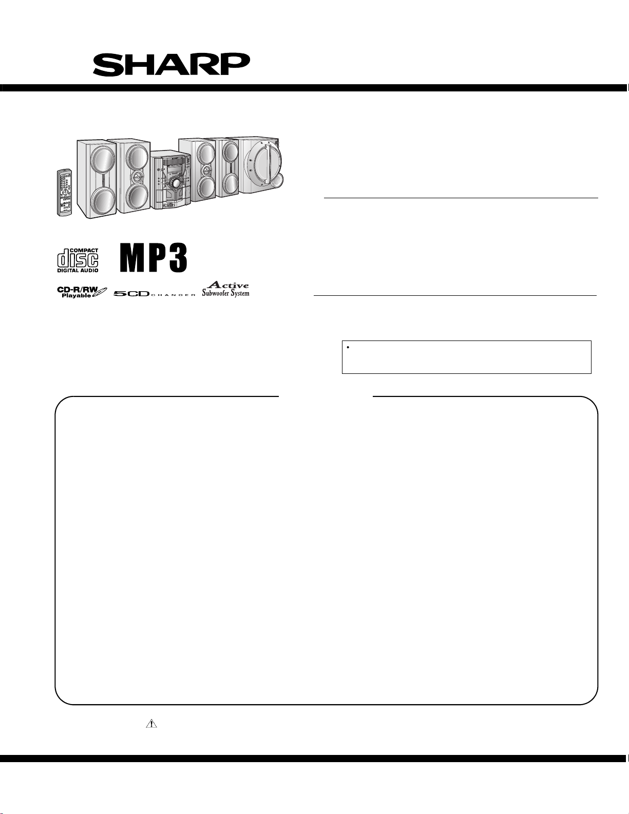
CD-G10000 Mini Component System consisting of CD-G10000
(main unit) and GBOXSA090AWM1 (rear speaker system).
CD-G10000
SPEAKER SYSTEM
MODEL
CP-G10000S Speaker System consisting of CP-G10000S
speaker system) and CP-SW10000S (active subwoofer).
In the interests of user-safety the set should be restored to its
original condition and only parts identical to those specified be
used.
CHAPTER 5. CIRCUIT DESCRIPTION
[1] Notes on schematic diagram .........................5-1
[2] Types of transistor and LED ..........................5-1
[3] Waveforms of CD circuit................................5-2
[4] Voltage...........................................................5-3
CHAPTER 6. CIRCUIT SCHEMATICS AND PARTS
LAYOUT
[1] Schematic diagram........................................6-1
[2] Wiring side of PWB......................................6-13
CHAPTER 7. FLOWCHART
[1] Troubleshooting.............................................7-1
CP-G10000S
(front
CHAPTER 3. MECHANISM BLOCKS
[1] Caution on disassembly ................................. 3-1
[2] Removing and reinstalling the main parts ........ 3-5
CHAPTER 4. DIAGRAMS
[1] Block diagrams............................................... 4-1
Parts marked with " " are important for maintaining the safety of the set. Be sure to replace these parts with specified ones for
maintaining the safety and performance of the set.
SHARP CORPORATION
CHAPTER 8. OTHERS
[1] Function table of IC .......................................8-1
[2] FL Display....................................................8-10
Parts Guide (CD-G10000)
Parts Guide (CP-G10000S)
This document has been published to be used
for after sales service only.
The contents are subject to change without notice.
Page 2
CD-G10000/CP-G10000S
TO EXPOSED
METAL PARTS
CONNECT TO
KNOWN EARTH
GROUND
TEST PROBE
0.15 mF
1.5 kohms
10 W
VTVM
AC SCALE
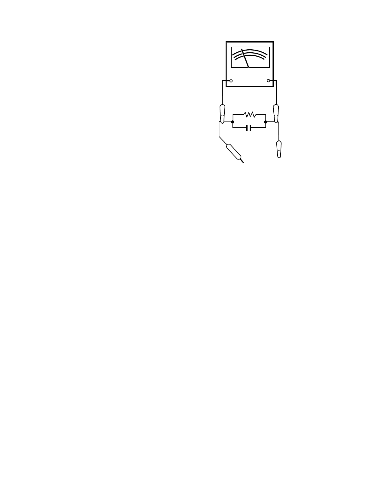
IMPORTANT SERVICE NOTES
BEFORE RETURNING THE AUDIO PRODUCT
BEFORE RETURNING THE AUDIO PRODUCT
(Fire & Shock Hazard)
Before returning the audio product to the user, perform the following
safety checks.
1. Inspect all lead dress to make certain that leads are not pinched or
that hardware is not lodged between the chassis and other metal
parts in the audio product.
2. Inspect all protective devices such as insulating materials, cabinet,
terminal board, adjustment and compartment covers or shields,
mechanical insulators etc.
3. To be sure that no shock hazard exists, check for leakage current in
the following manner.
* Plug the AC line cord directly into a 120 volt AC outlet.
* Using two clip leads, connect a 1.5 kohm, 10 watt resistor paralleled
by a 0.15 µF capacitor in series with all exposed metal cabinet parts
and a known earth ground, such as conduit or electrical ground connected to earth ground.
* Use a VTVM or VOM with 1000 ohm per volt, or higher, sensitivity to
measure the AC voltage drop across the resistor (See diagram).
* Connect the resistor connection to all exposed metal parts having a
return path to the chassis (antenna, metal cabinet, screw heads,
knobs and control shafts, escutcheon, etc.) and measure the AC
voltage drop across the resistor.
All check must be repeated with the AC line cord plug connection
reversed.
Any reading of 0.3 volt RMS (this corresponds to 0.2 milliamp. AC.) or
more is excessive and indicates a potential shock hazard which must
be corrected before returning the audio product to the owner.
– i –
Page 3
AudioCD-G10000/CP-G10000SService ManualCD-G10000/CP-G10000SMarketE
CHAPTER 1. GENERAL DESCRIPTION
[1] Specifications
FOR A COMPLETE DESCRIPTION OF THE OPERATION OF THIS UNIT, PLEASE REFER
TO THE OPERATION MANUAL.
CD-G10000 CP-G10000S
CD-G10000/CP-G10000S
General
Power source AC120V,60Hz
Power
consumption
Dimensions Width: 10-1/4" (260 mm)
Weight 23.0 lbs. (10.4 kg)
175 W
Height: 13" (330 mm)
Depth: 12-7/8" (326 mm)
CD player
Type 5-disc multi-play compact disc player
Signal readout Non-contact, 3-beam semiconductor laser
D/A converter 1-bit D/A converter
Frequency
response
Dynamic range 90 dB (1 kHz)
pickup
20 - 20,000 Hz
Amplifier
Output power
Front speakers 135 watts minimum RMS per channel into
Rear speakers 65 watts minimum RMS per channel into
Output terminals Front speakers: 8 ohms
Input terminals Game/ Auxiliary (audio signal):
8 ohms from 100 Hz to 20 kHz, 10% total
harmonic distortion
16 ohms from 5 kHz to 20 kHz, 10% total
harmonic distortion
Rear speakers: 16 ohms
Headphones: 16 - 50 ohms
(recommended: 32 ohms)
Subwoofer pre-out (audio signal):
200 mV/10 k ohms at 70 Hz
Video out: 1 Vp-p (75 ohms)
500 mV/ 47 k ohms
Game/Video: 1 Vp-p (75 ohms)
Tuner
Frequency range FM: 87.5 - 108.0 MHz
AM: 530 - 1,720 kHz
Cassette deck
Frequency
response
Signal/noise ratio 55 dB (TAPE 1, playback)
Wow and flutter 0.3 % (WRMS)
50 - 14,000 Hz (normal tape)
50 dB (TAPE 2, recording/playback)
Type 2-way type speaker system
2" (5 cm) tweeter 1
5-1/8" (13 cm) woofer 2
Maximum input
power
Rated input power 135 W
Impedance 8 ohms
Dimensions Width: 8-11/16" (220 mm)
Weight 12.1 lbs. (5.5 kg)/each
GBOXSA090AWM1
Type Full-range speaker system
Maximum input
power
Rated input power 65 W
Impedance 16 ohms
Dimensions Width: 7-7/8" (200 mm)
Weight 8.8 lbs. (4.0 kg)/each
CP-SW10000S
Power source AC 120 V, 60 Hz
Power
consumption
Output power 400 watts minimum RMS into 6 ohms from
Input terminals Subwoofer input (audio signal):
Speaker type 10" (25 cm) woofer
Impedance 6 ohms
Dimensions Width: 15-3/4" (400 mm)
Weight 47.6 lbs. (21.6 kg)
270 W
Height: 16-9/16" (420 mm)
Depth: 16-15/16" (430 mm)
4" (10 cm) speaker 2
130 W
Height: 16-9/16" (420 mm)
Depth: 16-15/16" (430 mm)
120 W
50 Hz to 120 Hz, 10% total harmonic distortion
200mV / 10 k ohms at 70 Hz
Height: 16-9/16" (420 mm)
Depth: 20-1/16" (510 mm)
Specifications for this model are subject to change without
prior notice.
1 – 1
Page 4
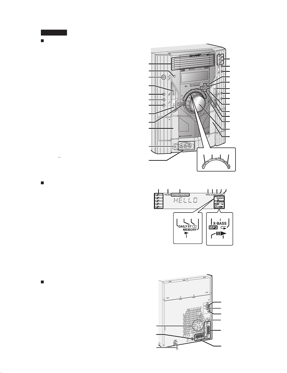
CD-G10000/CP-G10000S
[2] Names of parts
CD-G10000
Front panel
1. Disc Trays
2. Timer Indicator
3. Power On/Stand-by Button
4. Disc Track Up or Fast Forward, Tape 2 Fast Forward,
Tuner Preset Up, Time Up Button
5. Clock/Timer Button
6. Tuning Up Button
7. Tuning Down Button
8. Disc Track Down or Fast Reverse, Tape 2 Rewind,
Tuner Preset Down, Time Down Button
9. Equalizer Mode Select Button
10. Tape 1 Cassette Compartment
11. Headphone Jack
12. Game/Video Input Jacks
13. Disc Number Select Buttons
14. Disc Direct Play Button
15. Disc Tray Open/Close Button
16. Character Button
17. Enter Button
18. Disc Play or Repeat, Tape Play Button
19. Memory/Set Button
20. Tape 2 Record Pause Button
21. MP3 Disc Navigation Mode Select Button
22. Disc or Tape Stop Button
23. Cursor Buttons
24. Extra Bass/Demo Mode Button
25. Volume Control
26. Tape 2 Cassette Compartment
27. Tuner (Band) Button
28. CD Button
29. Tape (1 2) Button
30. Game/Video Button
10
11
12
13
1
2
3
4
5
6
7
8
9
14
15
16
17
18
19
20
21
22
23
24
25
26
28 29 3027
Display
1. Disc Number Indicators
2. MP3 Folder Indicator
3. MP3 Title Indicators
4. MP3 Total Indicator
5. Sleep Indicator
6. Timer Play Indicator
7. Timer Recording Indicator
8. Tape 2 Record Indicator
9. Daily Timer Indicator
10. FM Stereo Mode Indicator
11. FM Stereo Receiving Indicator
12. Memory Indicator
13. Tape Play Indicator
14. MP3 Disc Indicator
15. Extra Bass Indicator
16. Disc Repeat Play Indicator
17. Disc Pause Indicator
18. Disc Play Indicator
Rear panel
1. Cooling Fan
2. Subwoofer Pre-output Jack
3. AC Power Cord
4. FM 75 Ohms Antenna Terminal
5. FM Antenna Ground Terminal
6. AM Loop Antenna Jack
7. Video Output Jack
8. Front Speaker Terminals
9. Rear Speaker Terminals
4 5321 7 8
6
9
1110 12
13
14 15 16
18
17
4
5
6
7
1
8
2
1 – 2
3
9
Page 5
CD-G10000
CD-G10000/CP-G10000S
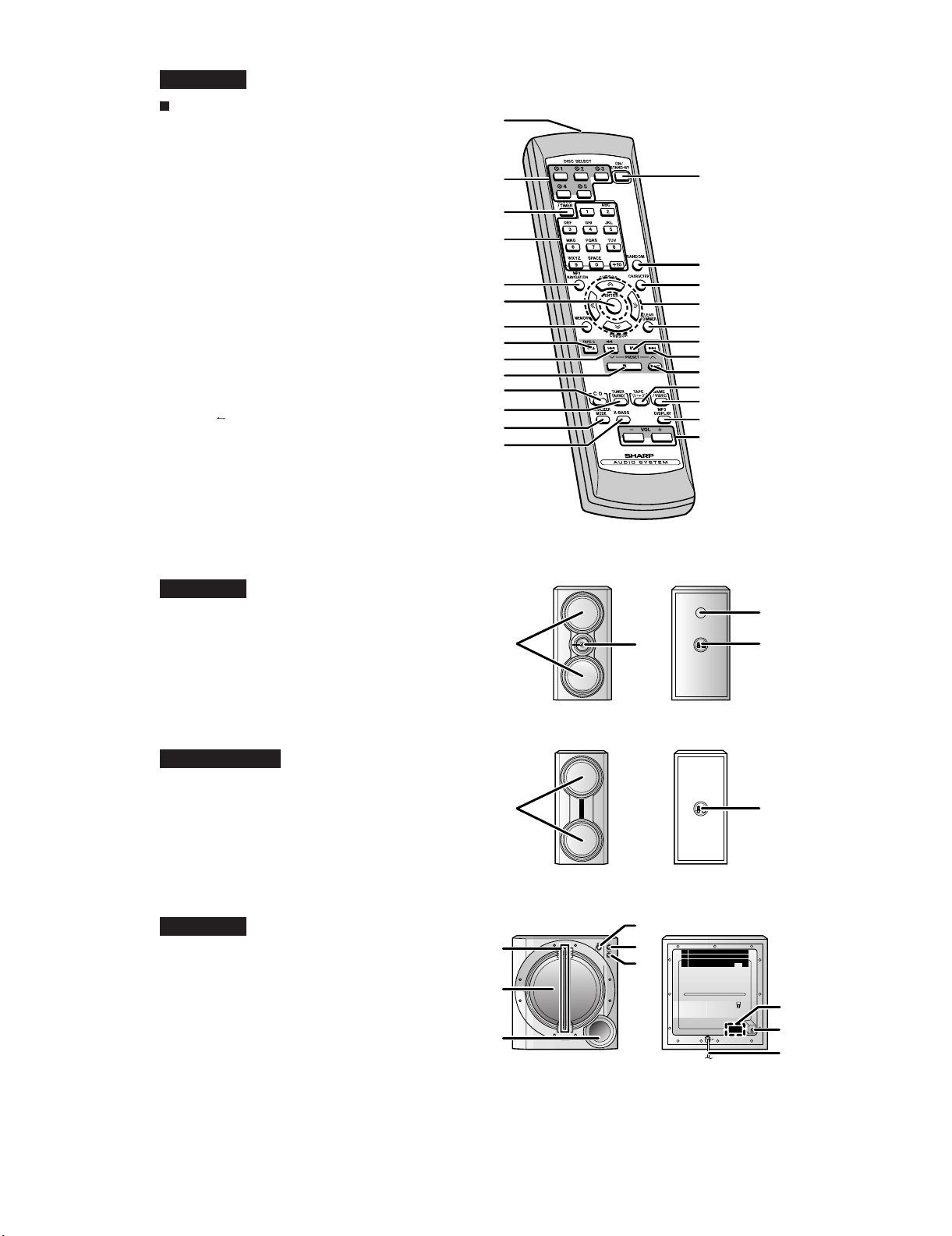
Remote control
1. Remote Control Transmitter
2. Disc Number Select Buttons
3. Clock/Timer Button
4. Character Input/Disc Direct Search Buttons
5. MP3 Disc Navigation Mode Select Button
6. Enter Button
7. Memory/Set Button
8. Tape 2 Record Pause Button
9. Disc Track Down or Fast Reverse, Tape 2 Rewind,
Tuner Preset Down, Time Down Button
10. Disc or Tape Stop Button
11. CD Button
12. Tuner (Band) Button
13. Equalizer Mode Select Button
14. Extra Bass Button
15. Power On/Stand-by Button
16. Disc Random Button
17. Character Button
18. Cursor Buttons
19. Disc Clear/Dimmer Button
20. Disc Pause Button
21. Disc Track Up or Fast Forward, Tape 2 Fast Forward,
Tuner Preset Up, Time Up Button
22. Disc Play or Repeat, Tape Play Button
23. Tape (1 2) Button
24. Game/Video Button
25. MP3 Disc Display Button
26. Volume Up and Down Buttons
10
11
12
13
14
1
2
15
3
4
16
5
6
7
8
9
17
18
19
20
21
22
23
24
25
26
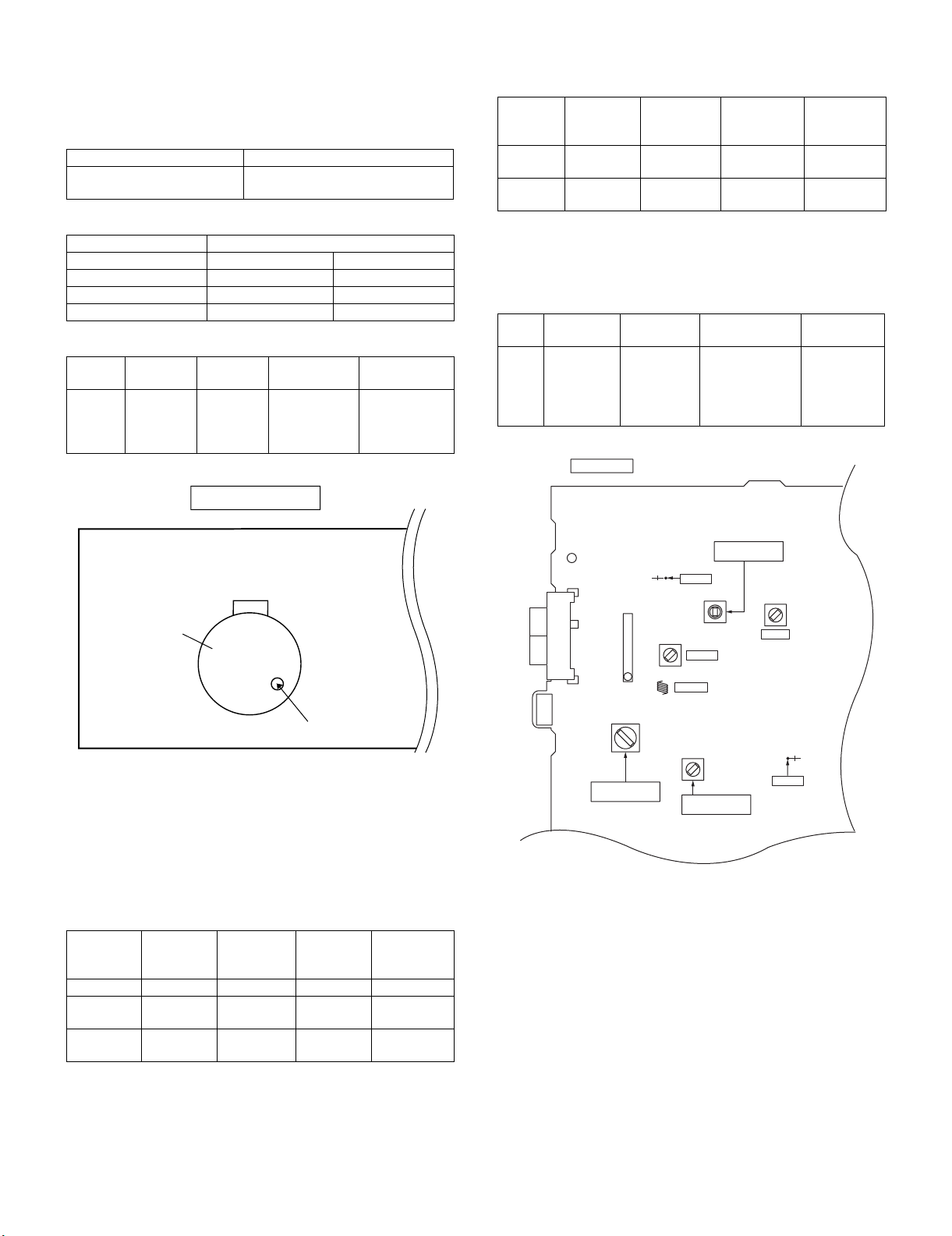
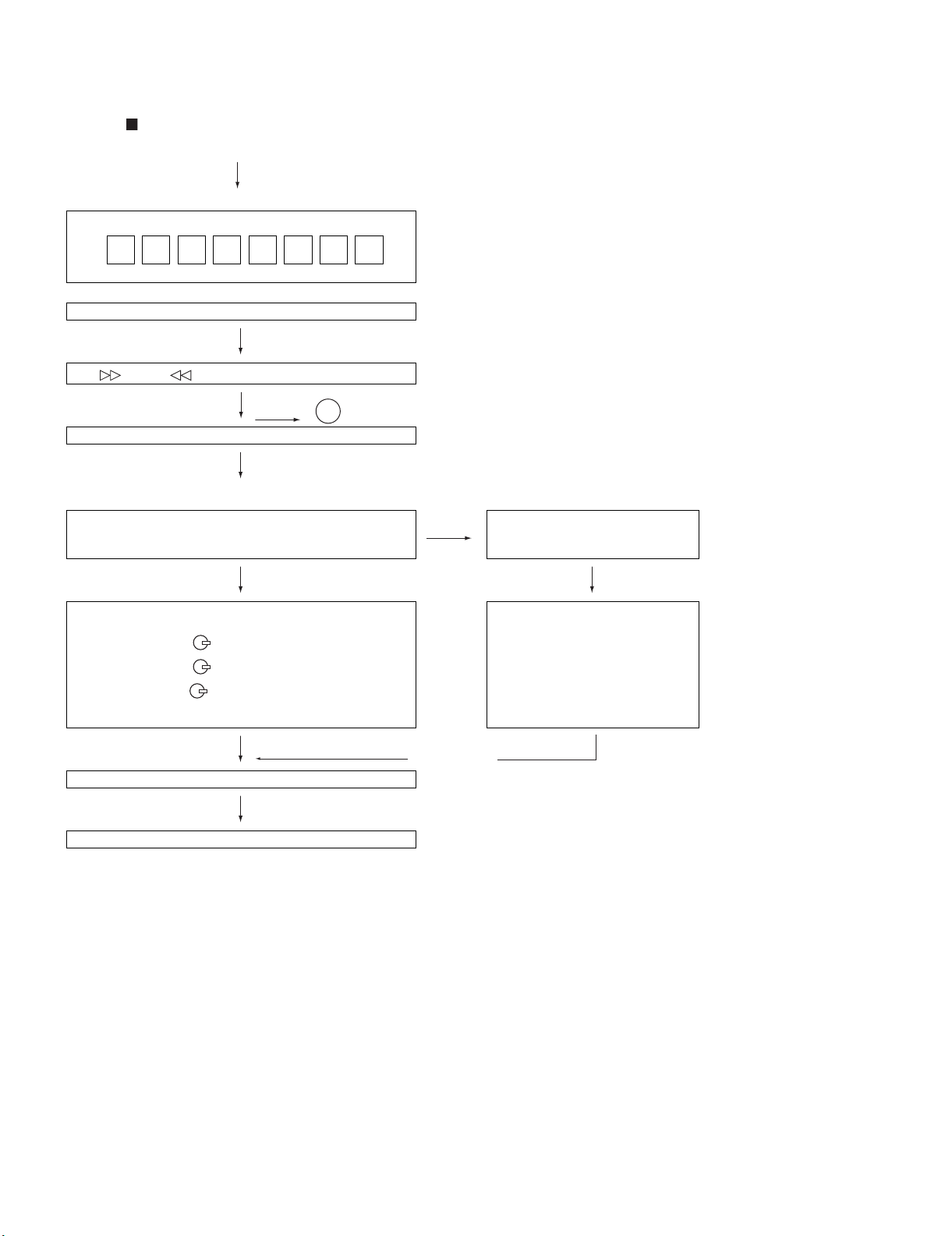
CP-G10000S
1. Woofers
2. Tweeter
3. Bass Reflex Duct
4. Speaker Terminals
GBOXSA090AWM1
1. Full-range Speakers
2. Speaker Terminals
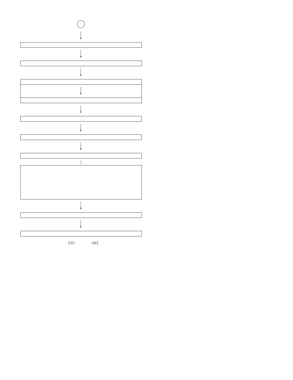
CP-SW10000S
1. Power Indicator
2. Subwoofer
3. Bass Reflex Duct
4. Power Switch
5. Volume Control
6. Crossover Frequency Control
7. Cooling Fan
8. Subwoofer Input Jack
9. AC Power Cord
3
1
2
1
4
2
4
1
5
6
2
7
3
8
9
1 – 3
Page 6
CD-G10000/CP-G10000S
AM IF
FM RF
TP301
TP302
FM IF
T301
T302
R356
R381
T303
T306
IC301
L312
T351
CNP301
AM LOOP ANTENNA
SO302
FM ANTENNA
TERMINAL
FM BAND
COVERAGE fL
AM BAND
COVERAGE fL
AM TRACKING
fL
MAIN PWB
1
AudioCD-G10000/CP-G10000SService ManualCD-G10000/CP-G10000SMarketE
CHAPTER 2. ADJUSTMENTS
•FM RF
Signal generator: 1 kHz, 40 kHz dev., FM modulated
[1] Mechanism section
• Driving Force Check
Torque Meter Specified Value
Play: TW-2111 Tape 1: Over 80 g
Tape 2: Over 80 g
• Torque Check
Torque Meter Specified Value
Tape 1 Tape 2
Play: TW-2111 30 to 80 g.cm 30 to 80 g.cm
Fast forward: TW-2231 — 70 to 180 g.cm
— 70 to 180 g.cm
• Tape Speed
Normal
speed
Test Tape Adjust-
ing Point
MT T-111 Va ria ble
Resistor in
motor.
TAPE MECHANISM
Specified
Val ue
3,000 ± 30 Hz
Speaker
Instrument
Connection
Speaker Terminal (Load
resistance: 6
ohms)
Test
Stage
Frequency Frequency
Display
Setting/
Adjusting
Point
FM Band
Coverage
FM RF 98.00 MHz
— 87.50 MHz T301 (fL):
1.3 V ± 0.1 V
98.00 MHz L312 *2
(10-30 dB)
*1. Input: Antenna Output: TP301
*2. Input: Antenna Output: Speaker terminal
•FM IF
Signal generator: 10.7 MHz, FM modulated
Test
Stage
Frequency Frequency
Display
Setting/Adjust-
ing Point
IF 10.7 MHz 98 MHz T302 (Turn the
core of transformer T302
fully counter
clockwise)
Instrument
Connection
*1
Instrument
Connection
*1
Tape
Motor
Variable Resistor in motor
Figure 1
[2] Tuner section
fL: Low-range frequency
fH: High-range frequency
• AM IF/RF
Signal generator: 400 Hz, 30%, AM modulated
Test Stage Frequency Frequency
Display
Setting/
Adjusting
Parts
AM IF 450 kHz 1,720 kHz T351 *1
AM Band
Coverage
AM
Tracking
*1. Input: Antenna Output: TP302
— 530 kHz (fL): T306
990 kHz 990 kHz (fL): T303 *1
*2. Input: Antenna Output: TP301
1.1 ± 0.1 V
Figure 2 Adjustment Points
Instrument
Connection
*2
2 – 1
Page 7
[3] TEST MODE
• Setting the test mode
During stand-by mode, press ON/STAND-BY button while pressing
down the button and X-BASS/DEMO button. then, press the CD
button to enter the test mode.
CD-G10000/CP-G10000S
C D T E S T
OPEN/CLOSE operation is using manual. IL isn’t done
<< >>,<< >>buttons make pick's slide possible.
to page 2-3
<<PLAY>> key input.
Do TOC IL. Do normal play.
When these following key is input into PLAY key, track number can be appoint directly.
<< 1 >> key: Track 4
<< 2 >> key: Track 9
<< 3 >> key: Track 15
A
IL isn’t done
IL isn’t done
<<MEMORY>>
key input.
Adjustment result automatically will
display as below for each 2 sec:
a) “FOF_XXXX”
b) “TOF_XXXX”
c) “TBAL_XX”
d) “TGAN_XX”
f) “FGAN_XX”
g) “RFLS_XX”
<<STOP>> key input.
STOP
explanation:
a) Focus off set = “FOF_XXXX”
b)Tracking off set = “TOF_XXXX”
c)Tracking balance = “TBAL_XX”
d)Tracking Gain = “TGAN_XX”
f) Focus Gain = “FGAN_XX”
g) RF level shift = “RFLS_XX”
VOL — Last memory
P. G E Q — FL A T
X-BASS — OFF
To cancel: Power OFF
––––––––
2 – 2
Page 8
CD-G10000/CP-G10000S
<<MEMORY>> key input.
Laser ON.
<<MEMORY>> key input.
Tracking OFF play at that specific point.
<<MEMORY>> key input.
Tracking ON play from that specific point.
A
<<MEMORY>> key input.
Adjustment result automatically will display as below for each 2 sec:
a) “FOF_XXXX”
b) “TOF_XXXX”
c) “TBAL_XX”
d) “TGAN_XX”
f) “FGAN_XX”
g) “RFLS_XX”
<<STOP>> key input.
STOP
Sliding the PICKUP with<< >>, << >> button must only be
in STOP mode.
explanation:
a) Focus off set = “FOF_XXXX”
b)Tracking off set = “TOF_XXXX”
c)Tracking balance = “TBAL_XX”
d)Tracking Gain = “TGAN_XX”
f) Focus Gain = “FGAN_XX”
g) RF level shift = “RFLS_XX”
VOL — Last memory
P. G E Q — FL A T
X-BASS — OFF
To cancel: Power OFF
2 – 3
Page 9
CD-G10000/CP-G10000S
[4] CD SECTION
• Adjustment
Since this CD system incorporates the following automatic adjustment functions, readjustment is not needed when replacing the
pickup. Therefore, different PWBs and pickups can be combined
freely.
Each time a disc is changed, these adjustments are performed
automatically. Therefore, playback of each disc can be performed
under optimum conditions.
Items adjusted automatically
1) Offset adjustment (The offset voltage between the head amplifier
output and the VREF reference voltage is compensated inside the
IC.)
* Focus offset adjustment
* Tracking offset adjustment
2) Tracking balance adjustment
3) Gain adjustment (The gain is compensated inside the IC so that the
loop gain at the gain crossover frequency will be 0 dB.)
* Focus gain adjustment
* Tracking gain adjustment
[5] CD section
CD Error code description
Error Explanation
01 When Pickup set inner position, inner switch cannot detect
'ON' level for 10 secs.
10* CAM error. Can't detect CAM switch when CAM is moving.
11* When it detect cam operation error during initialize pro-
cess.
20* TRAY error. Can't detect TRAY switch when TRAY is mov-
ing.
21* When it detect TRAY operation error during initialize pro-
cess.
31 When it change to CD function, DSP cannot read initial
data.
* 'CHECKING'
If Error is detected, 'CHECKING' will be displayed instead of 'ERCD**'. 'ER-CD**' display will only be displayed when error had been
detected for the 5th times.
[6] Standard Specification of Stereo System Error Message Display Contents
Error Contents Display Notes
CD Pickup Mechanism Error. 'ER-CD01' PU-IN SW Detection NG.
CD Changer Mechanism Error. 'ER-CD**' (*) 10: CAM SW Detection NG during normal operation
11: CAM SW Detection NG during initialize process
20:TRAY SW Detection NG during normal operation
21:TRAY SW Detection NG during initialize process
CD DSP Communication Error. 'ER-CD31' DSP COMMUNICATION ERROR.
Focus Not Match/IL Time Over. 'NO DISC'
TUNER PLL Unlock. PLL Unlock.
(*) CHECKING:
If CD changer mechanism error is detected, ‘CHECKING’ will be display instead of ‘ER-CD**’. ‘ER-CD**’ display will only be display when
error had been detected for the 5 th times.
Speaker abnormal detection and +B PROTECTION display
In case speaker abnormal detection or +B PROTECTION had
occurred, it can be check by pressing ‘POWER’, ‘ ’ and ‘X-BASS’
button. MicroComputer version number will displayed as “XM******”.
Press ‘GAME/VIDEO’ button during version number display and then
press ‘POWER’, ‘MEMORY/SET’ and ‘GAME/VIDEO’ button. Display
will show “S** B**”. S is referring to speaker abnormal detection and B
is referring to +B PROTECTION. ** is in hex valve.
FM 87.5 MHz
BEFORE TRANSPORTING THE UNIT
The following process need to be taken after set tapering/parts
replacement.
1. Press the ON/STAND-BY button to enter stand-by mode.
2. While pressing down the button and the X-BASS/DEMO button, press the ON/STAND-BY button. The Micro Computer version
number will be displayed as “XM******”.
3. Press OPEN/CLOSE button until “WAIT”→ “FINISHED” appears.
4. Unplug the AC cord and the unit is ready for transporting.
+B PROTECTION is condition when irregular process occur on power
supply line.
2 – 4
Page 10
CD-G10000/CP-G10000S
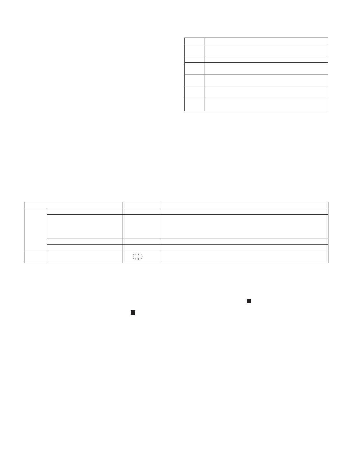
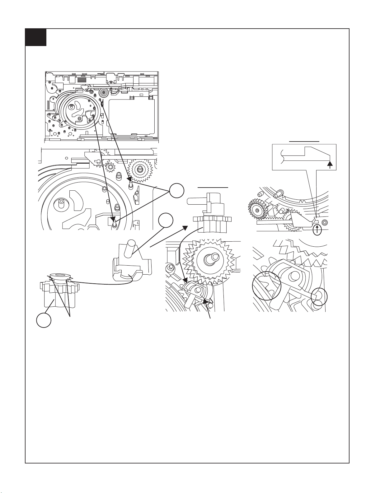
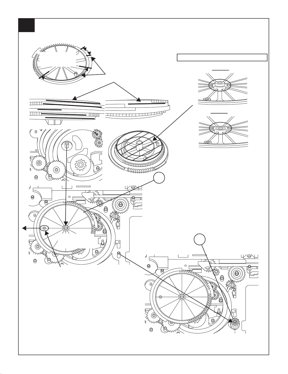
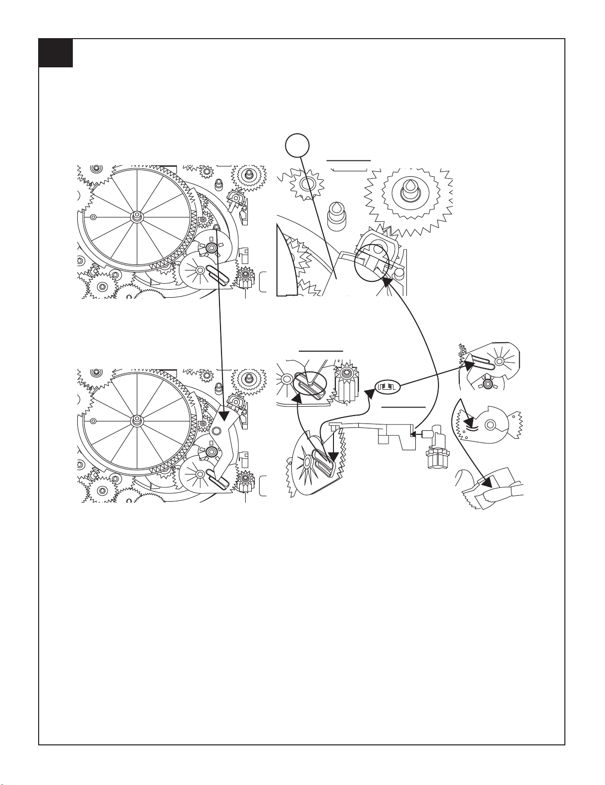
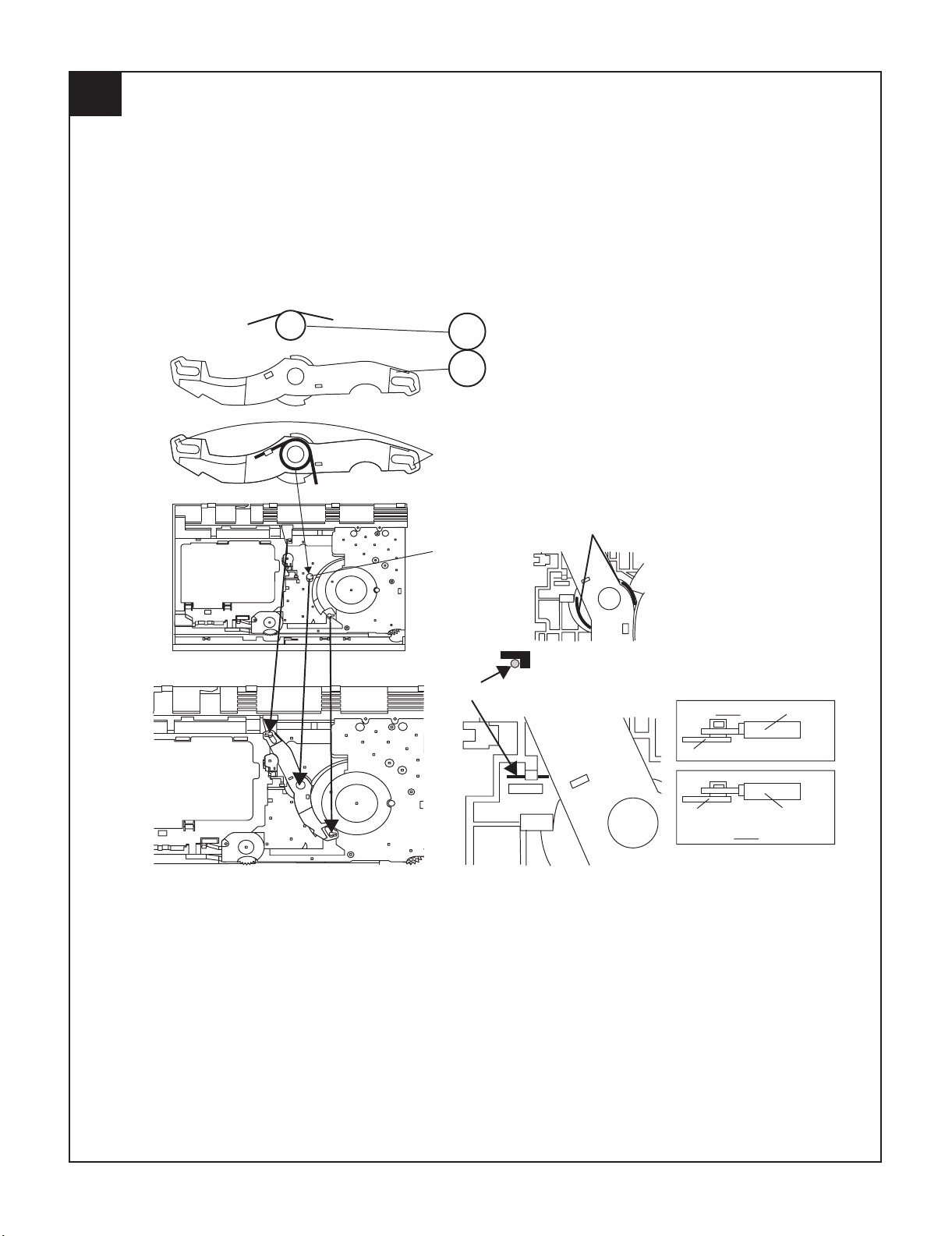
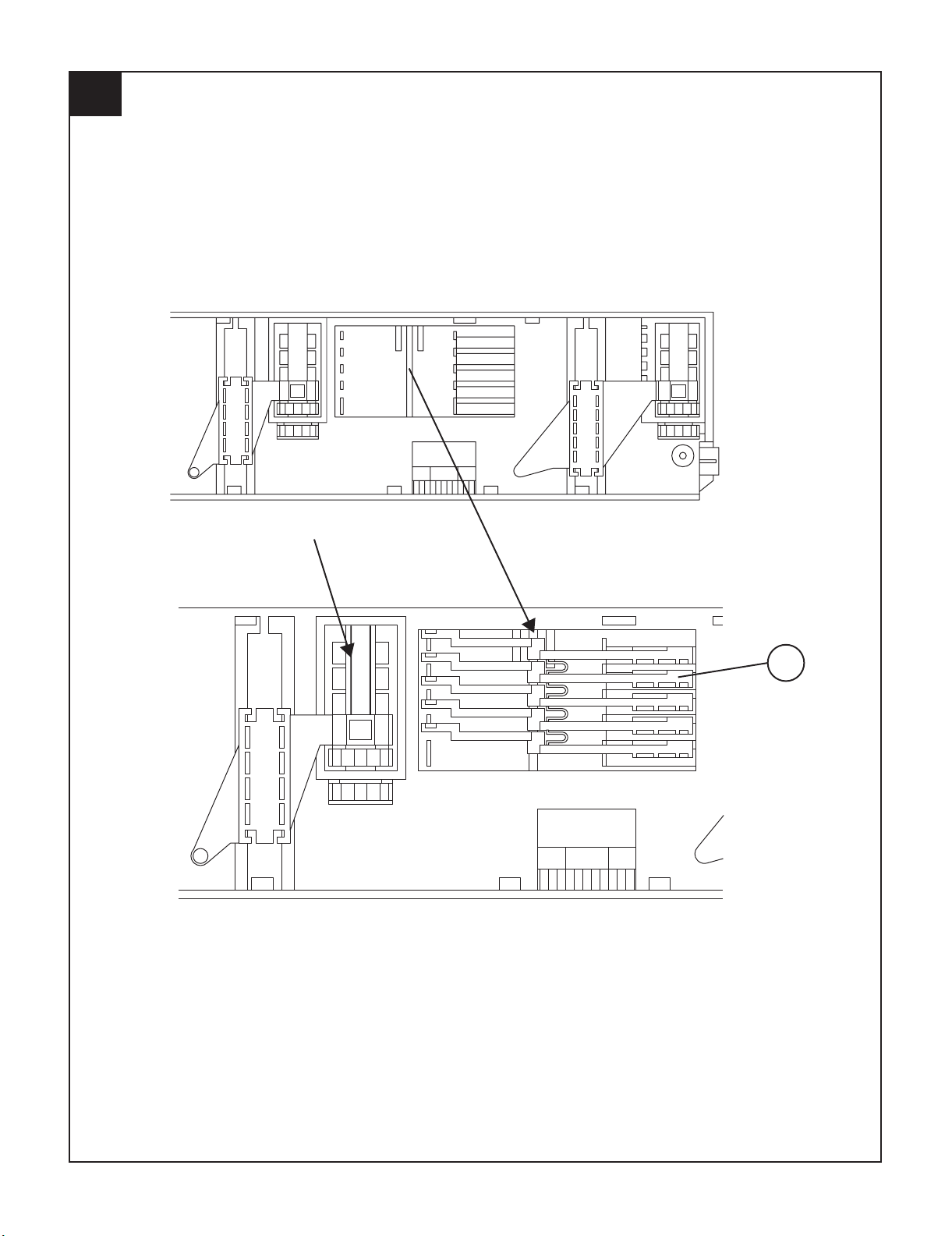
[7] CD Changer mechanism section
• A number in the drawing sheet is the number of the parts guide
(CHANGER MECHANISM PARTS).
1
141
2 – 5
140
HALF GEAR
MUST ARRANGE AS SHOWN
Page 11
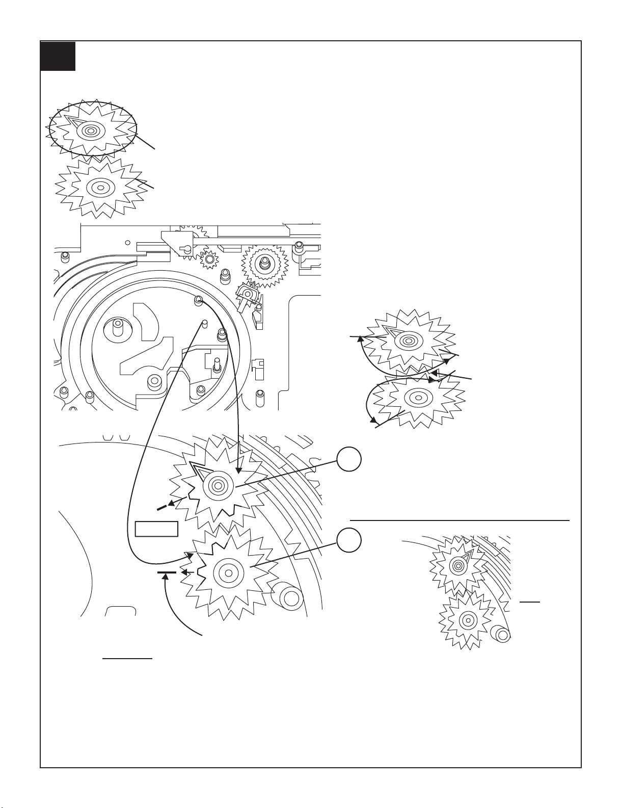
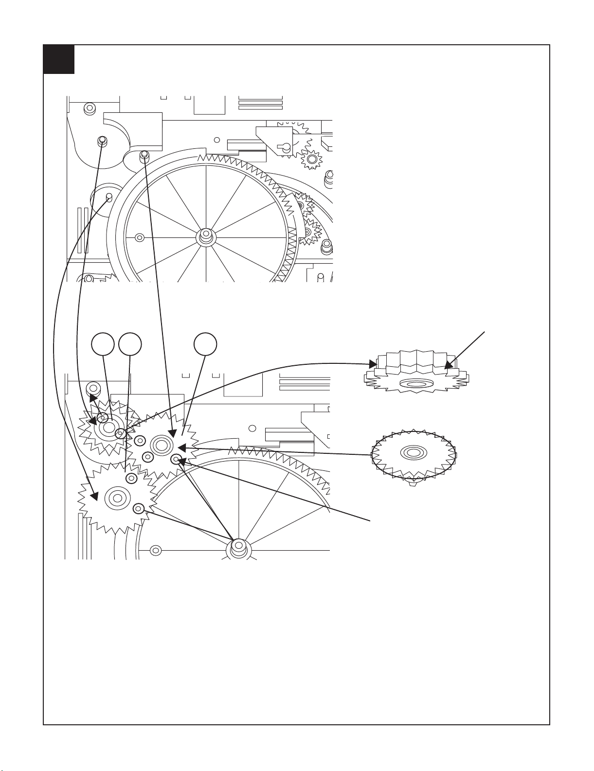
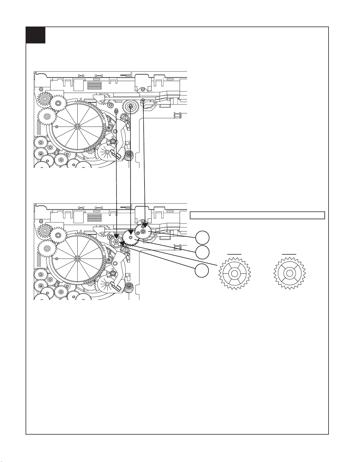
2
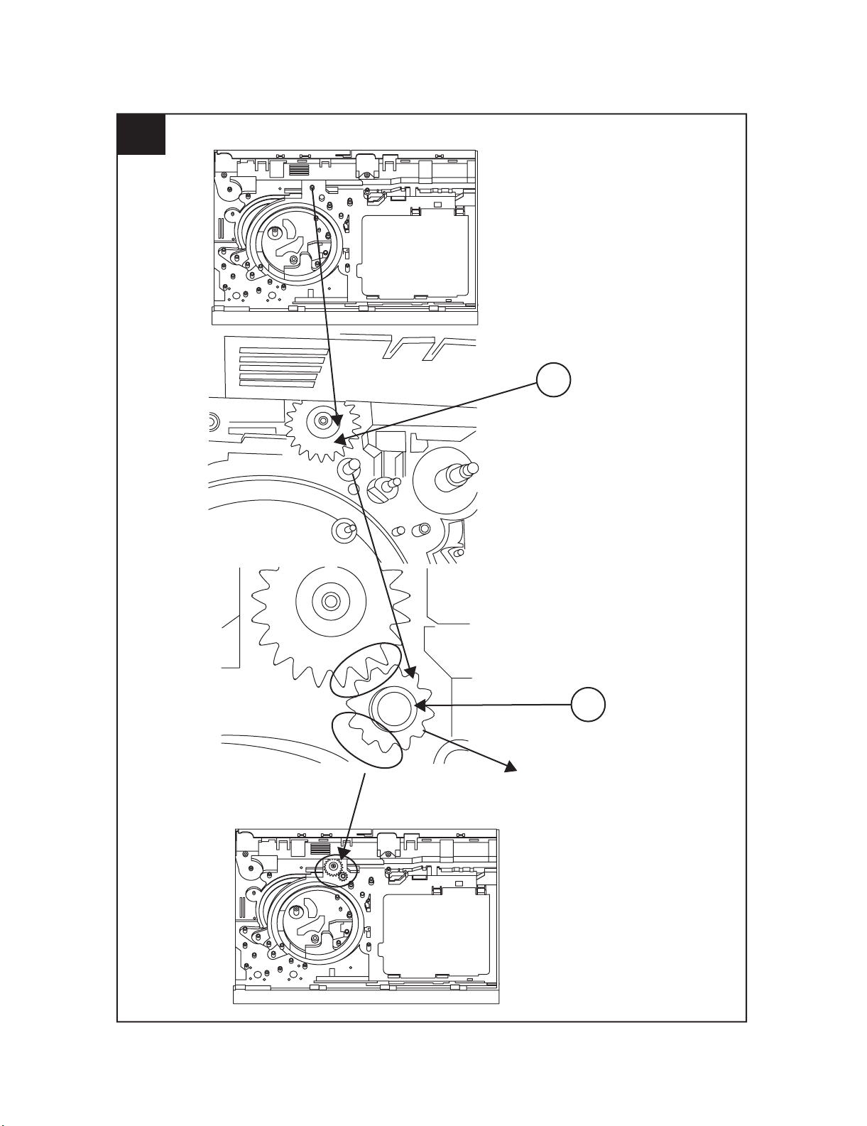
CD-G10000/CP-G10000S
139
APPLY SANKOL BEFORE FIX
FIX ITEM 1 ACCORDING TO THE
SHOWN PICTURE ABOVE
ROTATE MODE BIG GEAR UNTIL REACH AS SHOWN IN PICTURE
2 – 6
Page 12
CD-G10000/CP-G10000S
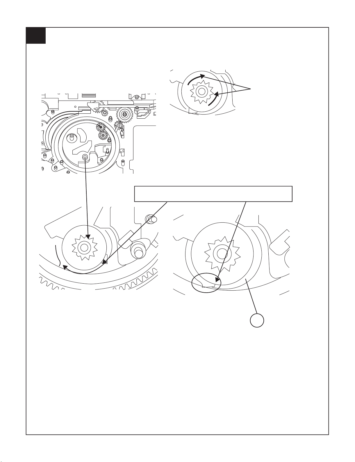
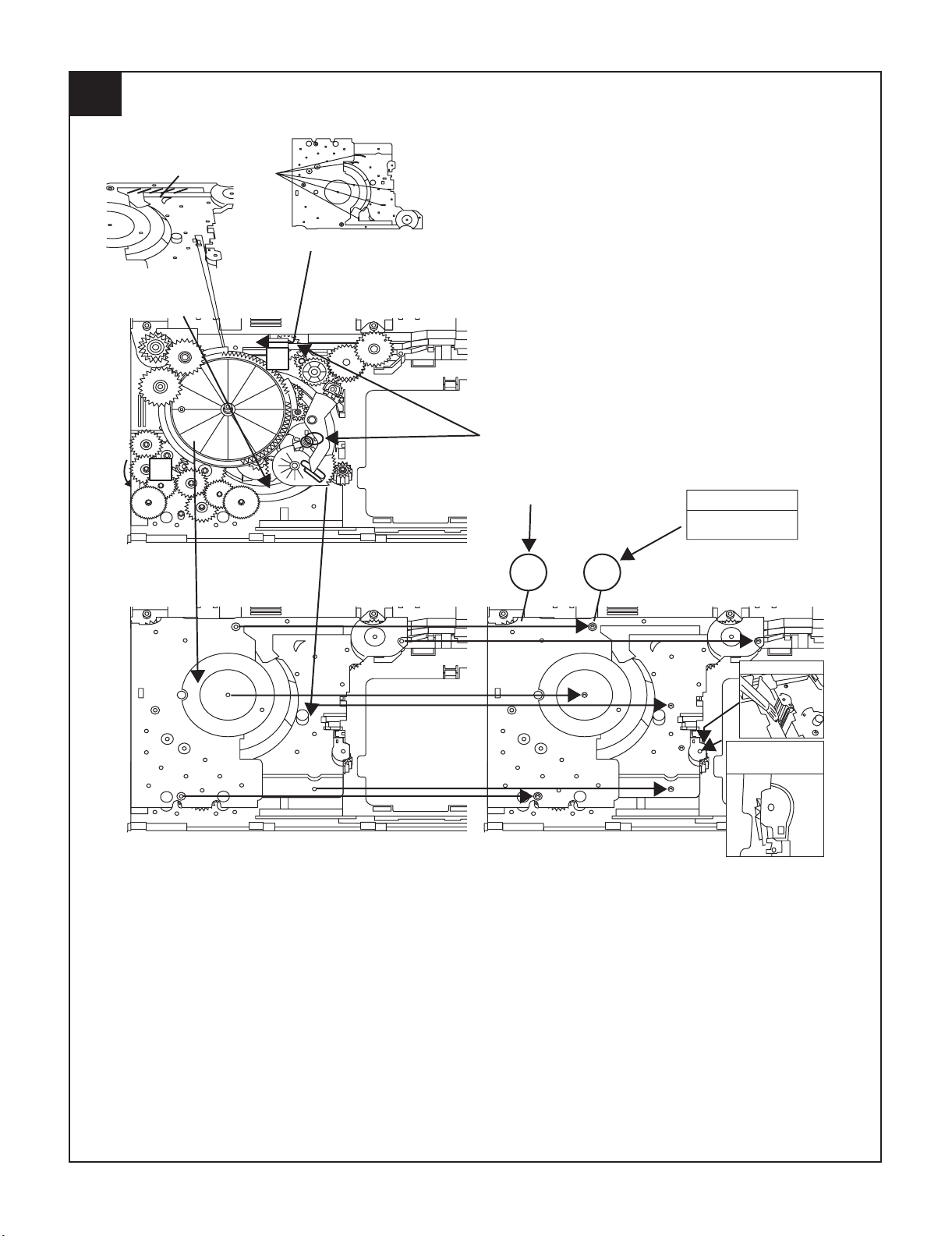
3
143
APPLY GREASE
112
PULL THE LEVER UNITIL
REACH THE ARROW MARK
2 – 7
Page 13
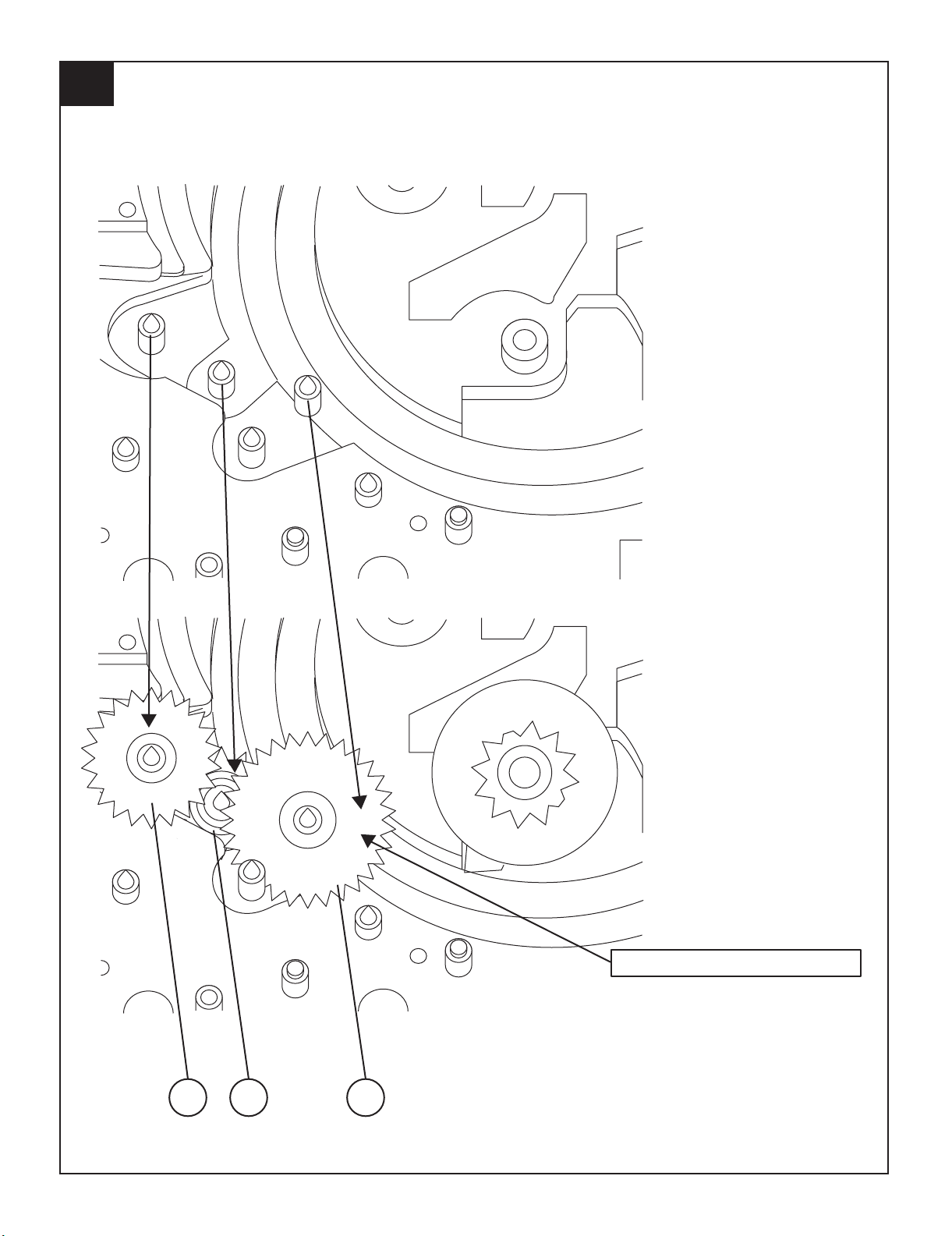
4
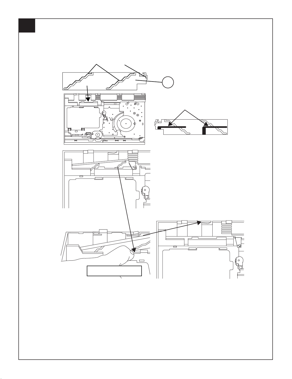
CD-G10000/CP-G10000S
FIGURE 2
FIGURE 1
152
142
APPLY GREASE
118
SLOT CLAMP SW ARM INSIDE BASE SLOT
2 – 8
Page 14
CD-G10000/CP-G10000S
5
APPLY GREASE AT BOTTOM SIDE
OF GEAR FOLLOW MARKING
NO NEED APPLY GREASE AT BOTTOM
SIDE
FIGURE 1
APPLY GREASE AT
TOP SIDE OF GEAR
FOLLOW MARKING
127
OTHER THAN FIGURE 1 DIRECTION ALL N.G
O.K
128
N.G
BLACK MARK
2 – 9
Page 15
6
CD-G10000/CP-G10000S
APPLY GREASE AT
HALF GEAR AREA
ROTATE CLOCKWISE UNTIL REACH HERE (MAXIMUM)
129
2 – 10
Page 16
CD-G10000/CP-G10000S
7
CHANGE COLOR TO BLACK
150151148
2 – 11
Page 17
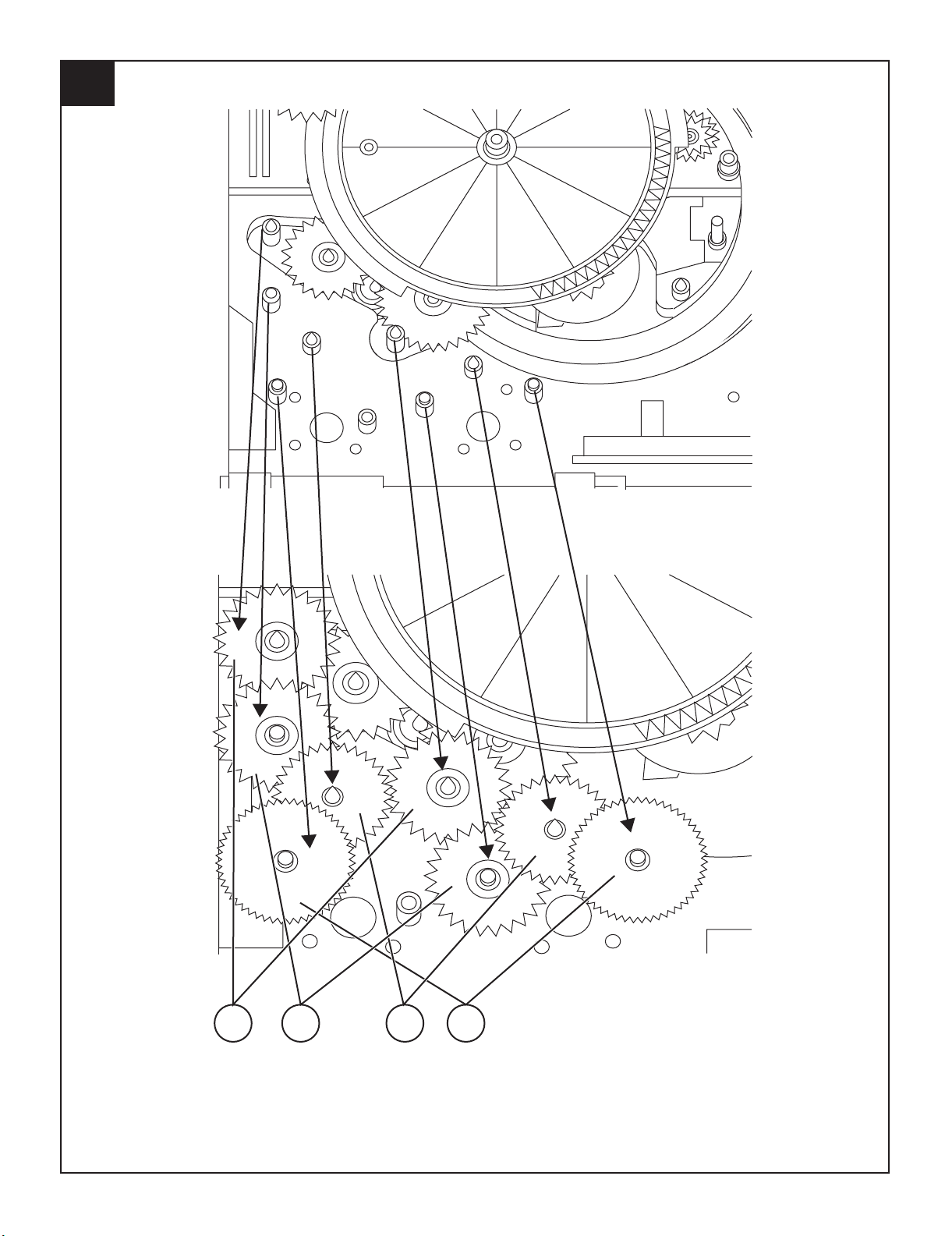
8
CD-G10000/CP-G10000S
TRAY BIG GEAR
CHANGE COLOR
TO BLACK
MUST FREE FROM GREASE THE SHOWN AREA
O.K
GREASE APPLICATION LENGTH
GREASE APPLICATION PORTION
N.G
124
TRAY BIG GEAR
CHANGE COLOR
TO BLACK
SHOWN HOLE MUST FACING ARROW DIRECTION
131
2 – 12
Page 18
CD-G10000/CP-G10000S
9
138 126 125
APPLY GREASE AT
BOTTOM SIDE ONLY
TR-RE JOINT GEAR C
APPLY GREASE ONLY AT TOP SIDE GEAR
MUST FIX ACCORDING TO T HE HOLE'S
2 – 13
Page 19
10
CD-G10000/CP-G10000S
148 147 146 145
2 – 14
Page 20
CD-G10000/CP-G10000S
11
121
144
WHEN FIXING ITEM 2 MUST FOLLOW AS SHOWN
APPLY GREASE
130
2 – 15
Page 21
12
CD-G10000/CP-G10000S
117
FIGURE 2
FIGURE 1
APPLY GREASE
FIGURE 3
APPLY GREASE SC141
2 – 16
Page 22
CD-G10000/CP-G10000S
13
ITEM 2 , 3 MUST APPLY GREASE ON TOP SIDE GEAR ONLY
134
GEAR 112 GEAR 112
133
132
O.K
TOP VIEW AFTER
ASSY
N.G
FIX REVERSE N.G
2 – 17
Page 23
14
APPLY GREASE BEFORE FIX
A
MOVE 112 UNTIL TOUCH THE WALL
B
DURING GEAR A ROTATE
MUST PRESS SHOWN AREA
AND LEVER B WILL MOVE
ARROW DIRECTION THEN
FIX PART 108
CD-G10000/CP-G10000S
SCREW TORQUE
+0.5
2 kgf-cm
-0
108 803 x6
APPLY GREASE
CONFIRM WHETHER
FIXED
PROPELY OR NOT
2 – 18
Page 24
CD-G10000/CP-G10000S
15
APPLY GREASE
115
BEHIND THE LEVER NEED TO APPLY GREASE
PULL IT THEN LEVER WILL
MOVE IN
2 – 19
Page 25
16
CD-G10000/CP-G10000S
123
115
APPLY GREASE
APPLY GREASE BEFORE FIX
APPLY GREASE
AT BOSS
SPRING MUST ARRANGE UNDER THE HOOK
BOARD R
BOARD R
O.K LR JOINT LEV
LR JOINT LEV
N.G
2 – 20
Page 26
CD-G10000/CP-G10000S
17
ASSY REVERSELY N.G
103 137 136
APPLY GREASE
BIG SLOT MUST FACING OUT
WHEN FIX & AFTER FIX TO BASE CHASSIS
AFTER ASSY CONFIRM THE FREE DROP
GEAR POSITION DURING FIXING
2 – 21
Page 27
18
CD-G10000/CP-G10000S
ASSY REVERSELY N.G
APPLY GREASE
114
135
136
BIG SLOT MUST FACING OUT
WHEN FIX & AFTER FIX TO BASE CHASSIS
AFTER ASSY CONFIRM THE FREE DROP
GEAR POSITION DURING FIXING
CONFIRM BOTH GEAR SIT PROPELY & LOCKED
2 – 22
Page 28
CD-G10000/CP-G10000S
19
AFTER FIX OUTER UP/DOWN LEVER HOLD SHOWN PORTION AND
MOVE UP/DOWN THEN CONFIRM LEVER GO INSIDE THE HOLE OR NOT
120
BIGGER SLOT FACING OUT
IF GO INSIDE HOLE
IS O.K
IF NO GO INSIDE HOLE IS N.G
119
BIGGER SLOT FACING OUT
2 – 23
Page 29
20
CD-G10000/CP-G10000S
BIG SLOT FACING OUT
110
2 – 24
Page 30
CD-G10000/CP-G10000S
21
PUSH THE LEVER ACCORDING TO ARROW
DIRECTION THEN FIX
WHEN FIX MAIN BASE ASSY FOLLOW ACCORDING TO O.K PICTURE
MAKE SURE MECHA HOLDER SHAFT FIX PROPELY TO LEVER
O.K
N.G
N.G
2 – 25
Page 31

22
CD-G10000/CP-G10000S
APPLY SANKOL
101
102
APPLY SANKOL AT TRAY SLIDING PORTION
APPLY SANKOL ON TOP
FIX TRAY NO 1 FIRST THAN
FOLLOW OTHER
APPLY SANKOL INSIDE THE SLOT
& OTHER SHOWN PORTION
RIB
RIB
COSMO GUIDE TRAY HAVE
MARKING AS SHOWN
2 – 26
Page 32

CD-G10000/CP-G10000S
23
GEAR UP/DOWN BOARD
111
APPLY GREASE AT INNER & OUTER GEAR SLIDING PORTION
WH EN FIX GEAR UP/
DOWN BOARD THE
TWO LEVER MUST AT
PARALLEL LINE &
POSITION AT TOP
MAX SIDE
2 – 27
AFTER ASSY GEAR UP/DOW N BOARD
Page 33

24
CD-G10000/CP-G10000S
SCREW TORQUE
+0.5
3 kgf-cm
-0
2 – 28
804
Page 34

CD-G10000/CP-G10000S
25
AFTER ASSY TOP PLATE
FIX THE FFC
FFC4
AFTER PUSH MAKE SURE SNAP PROPELY
AFTER FIX PUSH FOLLOW ARROW DIRECTION
BEFORE LOCK
AFTER LOCK
BACK
PORTION
107
122
BEFORE LOCK
PRESS IN
SLOT IN
BEFORE LOCK
AFTER LOCK
AFTER LOCK
MUST CONFIRM
MUST CONFIRM
2 – 29
Page 35

26
CD-G10000/CP-G10000S
O.K
N.G
CAUTION
1. MAKE SURE NO PW B CHIP INSIDE SET .( BEFORE
FIX MAKE SURE PW B NO DUST , GREASE & ETC )
803
2 – 30
Page 36

CD-G10000/CP-G10000S
27
THE TWO SLOT
MUST FREE FROM GREASE
APPLY GREASE BELOW
THE MARKING FOR
BOTH PORTION
ASSEMBLY SEQUENCE
1. APPLY GREASE TO MAIN BASE
GREASE APPLICATION AREA
ALL BOSS
APPLY GREASE
APPLY GREASE
CAUTION
TRAY SLIDING
AREA MUST
FREE FROM
GREASE
APPLY GREASE
APPLY GREASE AT WALL
APPLY GREASE
APPLY GREASE
APPLY GREASE
AT BOTH SLOT
105
APPLY GREASE AT 3 HALF MOON
1 RIB ONLY
APPLY GREASE
APPLY GREASE
INSIDE SLOT
2 – 31
Page 37

28
REFERENCE ONLY
MOTOR GEAR HEIGHT FROM
MAIN BASE 12.2
+
0.1
-
CD-G10000/CP-G10000S
0.1
-
+
12.2
MOTOR SCREWING HOLE
MUST HAVE GAP
M1,2
801
-0
13.8 + 0.2
SCREW TORQUE
1.5 + 0.5
-0
AFTER SCREW MOTOR,CONFIRM THE
ARRANGEMENT AS IN FIGURE 2
FIGURE 2
APPLY GREASE
2 – 32
Page 38

CD-G10000/CP-G10000S
29
APPLY SANKOL
3.1 + 0.1
SHAFT X 3 DIM AFTER INSERTION
MUST CONFIRM EVERYDAY
SANKOL APPLICATION AREA
109-2
APPLY GREASE AT THE SLIDING PORTION
114
116
UP / DOWN
HOLDER CHANGE
TO NATURE
COLOR
APPLY GREASE
2 – 33
Page 39

30
CD-G10000/CP-G10000S
BEFORE MELT IT
AFTER MELT IT ( MUST FLAT )
CHANGE COLOR
TO NATURE
WHEN FITTING STABILIZER PLATE TO STABILIZER,
ROTATE STABILIZER ANTI CLOCKWISE BY JIG
( BY HAND CANNOT X )
BELOW
AFTER ASSY TO HOLDER
STABILIZER NEED CLEAN
WITH ALCOHOL DISC
TOUCHING SURFACE
2 – 34
Page 40

CD-G10000/CP-G10000S
31
104
APPLY GREASE
MUST MAKE SURE SNAP PROPELY BOTH SIDE
ALL SURFACE MUST TOUCH
O.K N.G
GAP
N.G
2 – 35
Page 41

32
CD-G10000/CP-G10000S
NO GAP HAVE GAP
O.K N.G
2 – 36
Page 42

CD-G10000/CP-G10000S
AudioCD-G10000/CP-G10000SService ManualCD-G10000/CP-G10000SMarketE
CHAPTER 3. MECHANISM BLOCKS
[1] Caution on disassembly
Caution on Disassembly
Follow the below-mentioned notes when disassembling the unit and reassembling it, to keep it safe and ensure excellent performance:
1. Take cassette tape and compact disc out of the unit.
2. Be sure to remove the power supply plug from the wall outlet before starting to disassemble the unit.
3. Take off nylon bands or wire holders where they need to be removed when disassembling the unit. After servicing the unit, be sure to rearrange
the leads where they were before disassembling.
CD-G10000
STEP
Note 1:
After removing the connector for the optical pickup from the
connector, wrap the conductive aluminium foil around the
front end of the connector so as to protect the optical
pickup from electrostatic damage.
REMOVAL PROCEDURE
1 Top/Side Cabinet 1. Screw .................... (A1) x11
2 Changer Unit/ 1. Screw ...................... (B1) x2
Rear Panel B 2. Hook ........................ (B2) x2
3 Rear Panel A 1. Screw ...................... (C1) x6
with Fan motor/
Terminal PWB
4 Main PWB 1. Screw ...................... (D1) x2
5 Front Panel 1. Screw ...................... (E1) x2
6 Tape Mechanism 1. Open the cassette cover.
7 Display PWB 1. Knob ........................ (G1) x1
3. Flat Cable ................ (B3) x1
4. Socket ..................... (B4) x1
2. Socket .....................
3. Socket (C3) x1
2. Flat Cable ............... (D2) x1
3. Socket ..................... (D3) x4
4. Flat Wire .................. (D4) x1
5. Screw ...................... (D5) x4
2. Flat Wire .................. (E2) x1
3. Hook ........................
2. Screw ....................... (F1) x6
3. Flat Cable ................(F2) x1
2. Screw .................... (G2) x10
3. Hook (G3) x5
.....................
........................
(C2) x1
(E3) x2
8 Game Input PWB 1. Screw........................ (H1) x2
9 CD Servo PWB 1. Screw ...................... (J1) x2
10 Changer 1. Screw ...................... (K1) x4
Mechanism Unit 2. Changer Chassis .... (K2) x1
2. Flat Cable ............... (J2) x2
3. Socket ..................... (J3) x1
4. Hook ........................ (J4) x1
11 CD Mechanism 1. Screw ...................... (L1) x4
(C2)x1
Rear
Panel B
(B1)x2
M3x10mm
Rear
Panel A
Fan Motor
(C1)x6
M3x10mm
(C3)x1
Terminal
PWB
Main PWB
(B2)x1
Pull
Changer
Mechanism
Unit
(D2)x1
(D3)x1
(D3)x2
CD Servo
PWB
(D1)x1
M3x10mm
Front Panel
Lug Wire
Main PWB
(E2)x1
(B3)x1
(B4)x1
(B2)x1
Pull
(D1)x1
M3x10mm
(A1)x3
M3x10mm
Rear Panel B
Rear Panel A
Top/Side Cabinet
(A1)x5
M3x10mm
Front Panel
(A1)x3
M3x10mm
3 – 1
(E3)x1
(D4)x1
(D3)x1
Power PWB
(D5)x4
M3x6mm
Main
PWB
Front Panel
(E3)x1
(E1)x2
M3x8mm
Page 43

Tape
Mechanism
Lug Wire
(F2)x1
Front Panel
(K1)x4
M3x10mm
CD-G10000/CP-G10000S
(F1)x6
M3x10mm
(G2)x10
M2.6x10mm
Lug Wire
Front Panel
(H1)x2
M3x10mm
Display PWB
(G3)x5
Open
Cassette
Cover
(G1)x1
Game Input
PWB
(L1)x4
M2.6x10mm
(K2)x1
Changer
Mechanism
Unit
CD Mechanism
(J1)x2
M3x10mm
(J3)x1
(J2)x1
(J4)x1
(J2)x1
CD Servo
PWB
Changer
Mechanism
Unit
3 – 2
Changer
Mechanism
Unit
Page 44

CD-G10000/CP-G10000S
CP-G10000S
STEP
Screwdriver
REMOVAL PROCEDURE
1 Woofer 1. Front Panel .............. (A1) x1
2 Tweeter 1. Screw ...................... (B1) x2
Driver should
be pried away
from Speaker Box.
2. Screw ...................... (A2) x8
(A1)x1
Speaker Box Ass'y
GBOXSA090AWM1
STEP
REMOVAL PROCEDURE
1 Woofer 1. Front Panel .............. (A1) x1
Screwdriver
Driver should
be pried away
from Speaker Box.
2. Screw ...................... (A2) x8
(A1)x1
Speaker Box Ass'y
(A2)x4
M4x16mm
Tweeter
(B1)x2
M3x12mm
(A2)x4
M4x16mm
Woofer
Speaker Box Ass'y
Woofer
(A2)x4
M3.5x16mm
(A2)x4
M3.5x16mm
Speaker Box Ass'y
Woofer
Woofer
3 – 3
Page 45

CD-G10000/CP-G10000S
CP-SW10000S
STEP
REMOVAL PROCEDURE
1 Rear Cabinet 1. Screw (A1) x1
2. Screw ....................
2
Power PWB/Fan
Motor
1. Screw ...................... (B1) x8
2. Screw ...................... (B2) x2
3. Socket ..................... (B3) x5
......................
(A2) x13
4. Screw ...................... (B4) x2
3 Transformer PWB
1. Screw ...................... (C1) x2
2. Socket ..................... (C2) x3
4JackPWB
1. Screw ......................
2. Bracket ....................
(D1) x4
(D2) x1
3. Screw ...................... (D3) x1
4. Socket ..................... (D4) x1
5 Front Panel
1. Screw Cover ............
2. Catching Holder .......
(E1) x8
(E2) x8
3. Screw ...................... (E3) x8
4. Socket ..................... (E4) x2
6 Subwoofer
7 Volume PWB
1. Screw ......................
1. Screw ...................... (G1) x4
(F1) x8
2. Socket ..................... (G2) x3
8
Power Switch PWB
Speaker Box Ass'y
1. Screw ......................
Front Panel
(H1) x2
Washer
(D1)x4
M3x20mm
Transformer
PWB
(C1)x1
M3x10mm
(C2)x1
(D4)x1
(E2)x8
Speaker Box Ass'y
(C2)x2
(E3)x8
M4x40mm
(D2)x1
Jack PWB
(D3)x1
M3x8mm
(C1)x1
M3x10mm
Front Panel
Front Panel
(A1)x1
M3x10mm
(B3)x3
(B2)x2
M4x16mm
(B1)x4
M3x8mm
(A2)x13
M4x20mm
Speaker Box Ass'y
Rear Cabinet
Front Panel
(E1)x8
(F1)x8
M4x20mm
(H1)x2
M3x10mm
(G1)x4
M3x10mm
Volume PWB
Speaker Box Ass'y
Subwoofer
(E4)x1
Power Switch PWB
Front Panel
(G2)x3
(B1)x4
M3x8mm
(B4)x2
M3x14mm
(E4)x1
Power PWB
Fan Motor
(B3)x2
3 – 4
Page 46

CD-G10000/CP-G10000S
[2] Removing and reinstalling the main parts
1. TAPE MECHANISM SECTION
Perform steps 1 to 5 and 6 of the disassembly method to remove the
tape mechanism.
1.1. How to remove the record/playback and erase heads
(TAPE 2) (See Fig. 1)
1. When you remove the screws (A1) x 2 pcs., the recording/playback
head and three-dimensional head of the erasing head can be
removed.
TAPE 2
Clutch Ass'y
Pinch Roller
(C1)x1
Pull
<B>
<A>
Pinch
Roller
Pawl
Record/Playback
Head
Erase Head
(A1)x2
M2x9mm
Figure 1
1.2. How to remove the playback head (TAPE 1)(See Fig. 2)
1. When you remove the screws (B1) x 2 pcs., the playback head can
be removed.
TAPE 1
Clutch Ass'y
Playback
Head
Figure 3
1.4. How to remove the belt (TAPE 2) (See Fig. 4)
1. Remove the main belt (D1) x 1 pc., from the motor side.
2. Remove the FF/REW belt (D2) x 1 pc.
1.5. How to remove the belt (TAPE 1) (See Fig. 4)
1. Remove the main belt (E1) x 1 pc., from the motor side.
2. Remove the FF/REW belt (E2) x 1 pc.
Tape
Motor
TAPE 2
Main Belt
(D1)x1
TAPE 1
Main Belt
(E1)x1
TAPE 1
FF/REW
Belt
(E2)x1
TAPE 2
Main Belt
(D1)x1
FF/REW
Belt
(D2)x1
Tape
Motor
Main Belt
(E1)x1
Figure 4
1.6. How to remove the motor (See Fig. 5)
1. Remove the screws (F1) x 2 pcs., to remove the motor.
(B1)x2
M2x9mm
Figure 2
1.3. How to remove the pinch roller (TAPE 1/2) (See Fig. 3)
1. Carefully bend the pinch roller pawl in the direction of the arrow
<A>, and remove the pinch roller (C1) x 1 pc., in the direction of the
arrow <B>.
NOTE: When installing the pinch roller, pay attention to the spring
mounting position.
3 – 5
(F1)x2
M2.6x5mm
Figure 5
Tape
Motor
Clutch Ass'y
Page 47

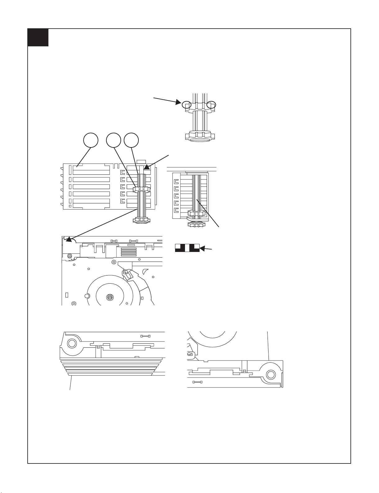
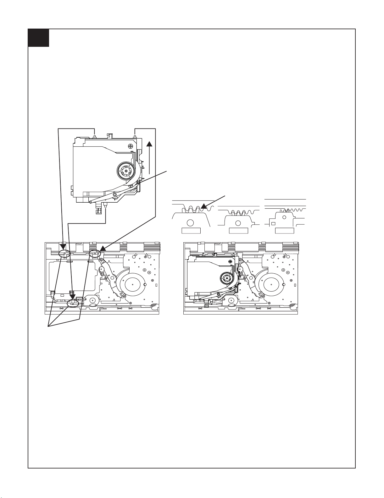
2. CD MECHANISM SECTION
Mark 1
(DISC 1)
(DISC 2)
(DISC 3)
(DISC 4)
(DISC 5)
Gear up down board
Mark 3 Mark 5
Mark 2 Mark 4
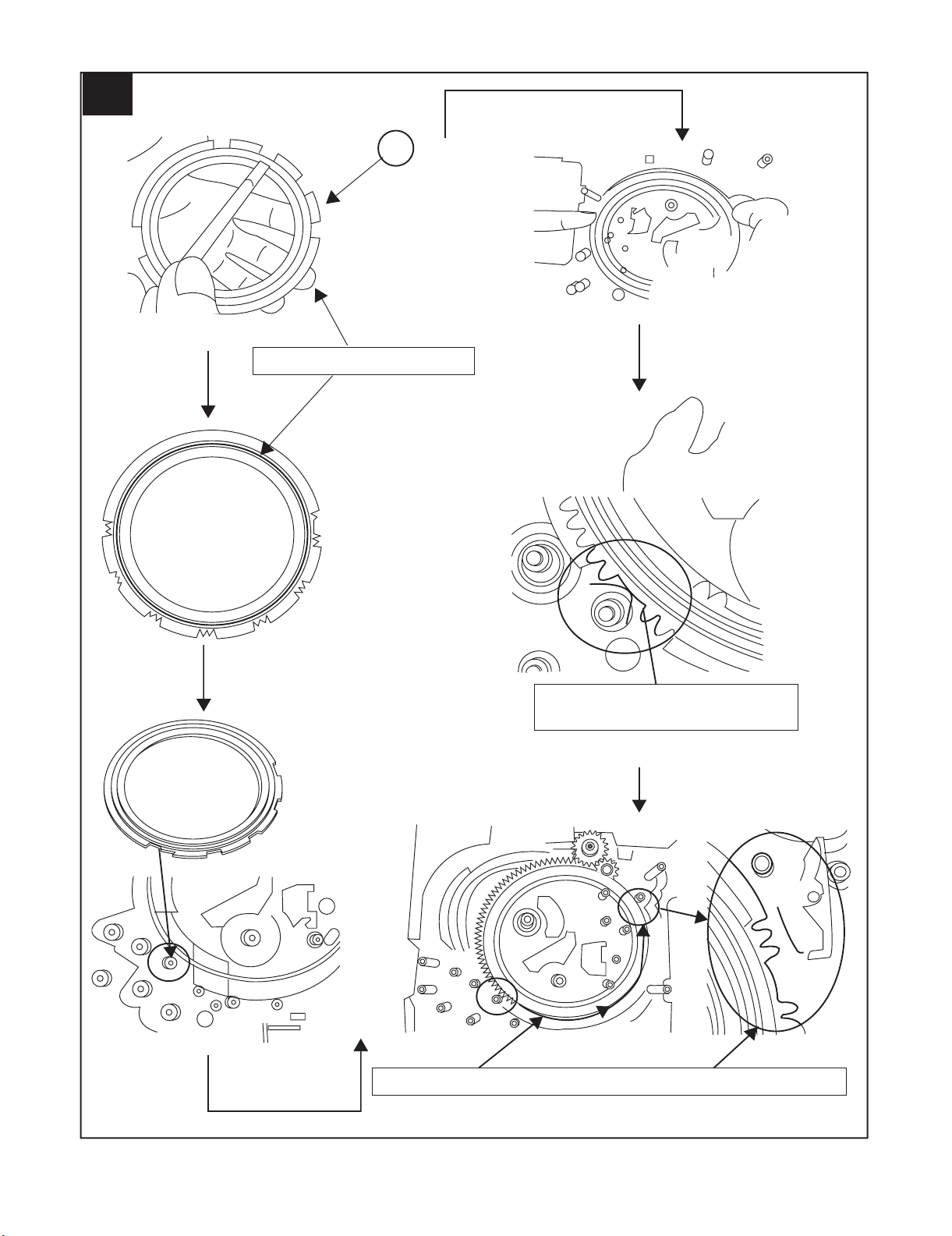
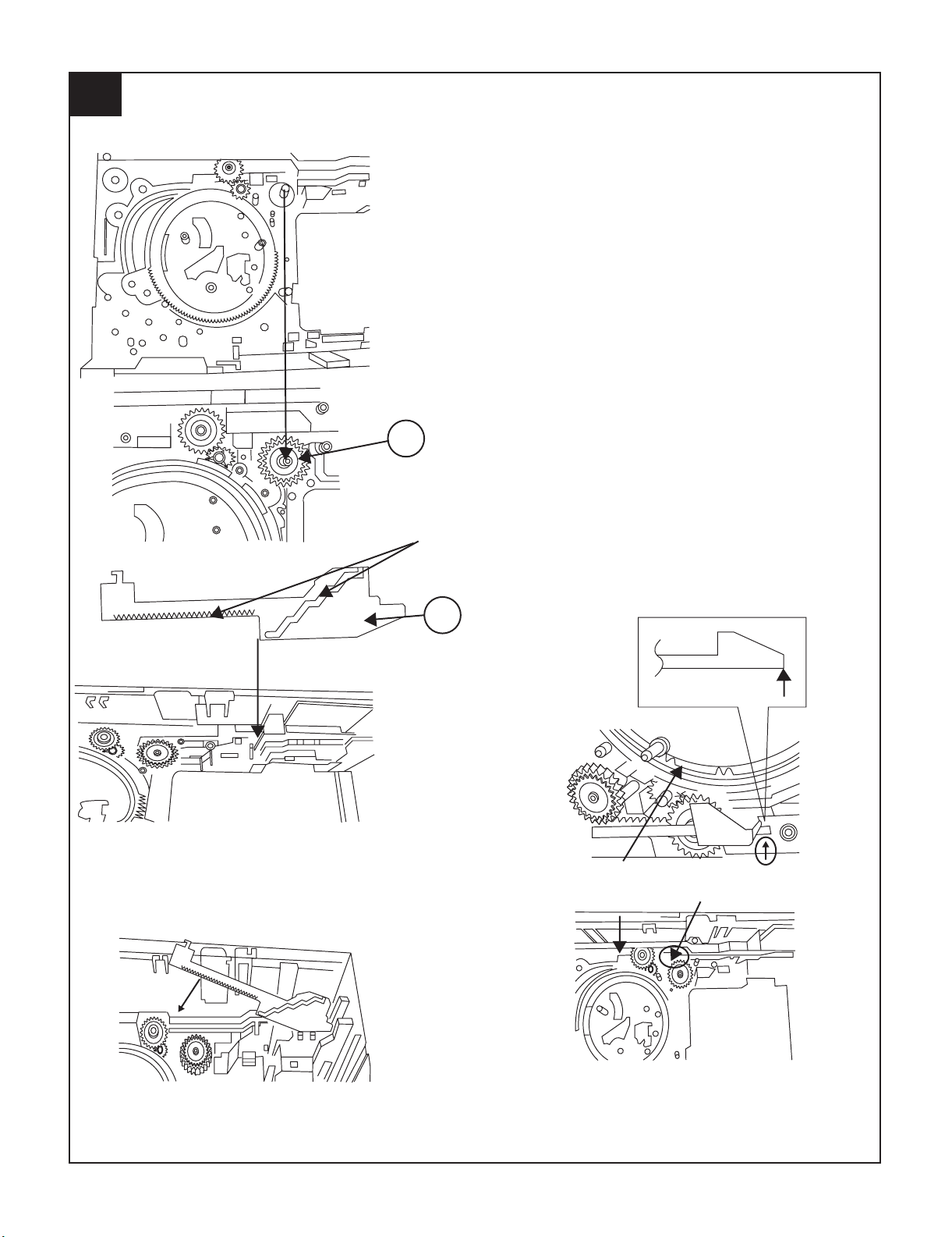
Perform steps 1, 2, 9 10 and 11 of the disassembly method to remove
the CD mechanism.
2.1. Remove the pickup. (See Fig. 1)
1. Remove the stop washer (A1) x 1 pc., to remove the gear (A2) x 1
pc.
2. Remove the screws (A3) x 2 pcs., to remove the shaft (A4) x 1 pc.
3. Remove the pickup.
NOTE: After removing the connector for the optical pickup from the
connector wrap the conductive aluminium foil around the front
end of connector so as to protect the optical pickup from electrostatic damage.
(A3)x2
M2.6x6mm
CD Mechanism
CD-G10000/CP-G10000S
Reduction gear C
Front Rear
Figure 3
2. In another case, if CD mechanism is at tray No.1 play position and
to remove CD located in tray No.3, the procedure is as follows:
If the gear up down board is located at tray No.1 position, then
rotate gear clock-wise until it at stock position. Rotate reduction
gear D clockwise (Figure 4) to move the CD mechanism to tray
No.3 position.This is confirmed by checking the gear up down
board position by the marking as indicated on the main chassis as
shown in Figure 5.
Shaft
(A4)x1
Gear
(A2)x1
Stop Washer
(A1)x1
Pickup Unit
Figure 1
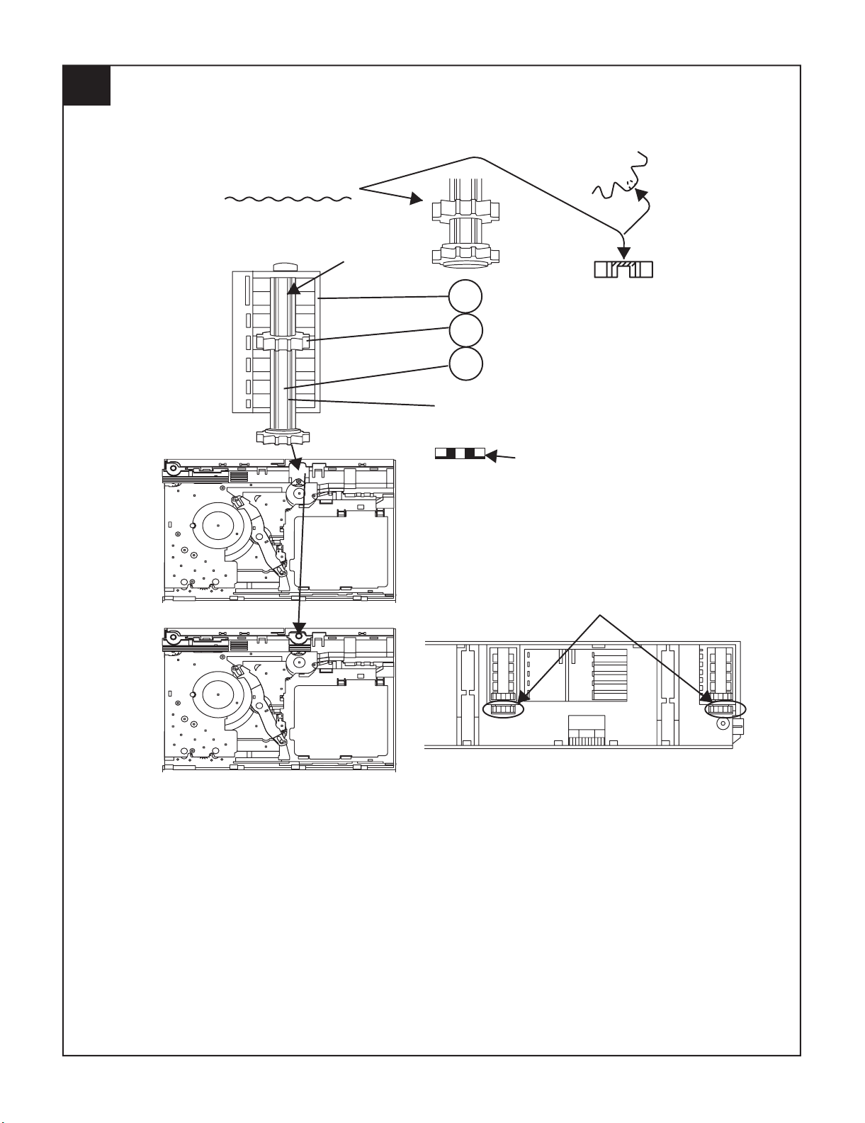
3. CHANGER MECHANISM SECTION
Perform steps 1, 2, 9 and 10 of the disassembly method to remove the
CD changer mechanism.
3.1. How to remove CD Disc (See Fig. 2~5)
1. When CD is at play position (Figure 2), rotate reduction gear C
clock-wise as shown in Figure 3 Until disc tray is at stock position,
then rotate further to eject the disc tray so that CD can be removed
from the tray.
CD Disc
Disc Tray
Guide Tray
Reduction gear D
Up Down
Figure 4
CD Disc
CD At play position.
CD At stalk position.
Figure 2
Figure 5
3 – 6
Page 48

CD-G10000/CP-G10000S
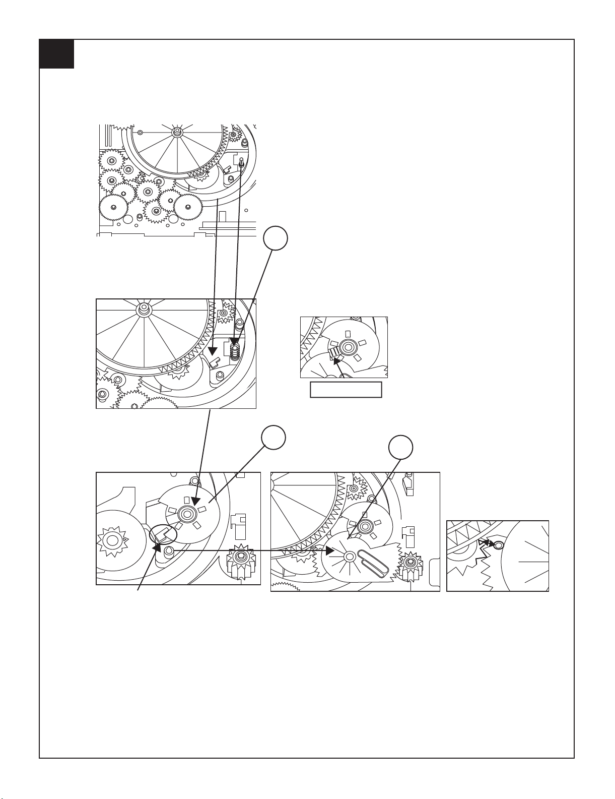
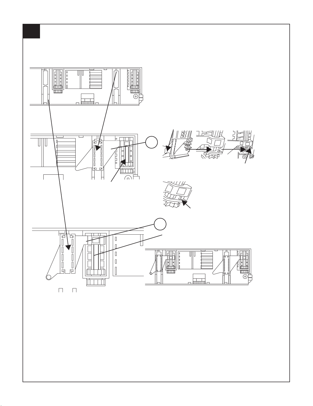
3.2. How to Remove the tray motor/main cam motor/5-
Changer Motor PWB (See Fig. 6)
1. Remove the screws (A1)x 2 pcs., to remove tray motor/main cam
motor/5-Changer Motor PWB.
Changer Mechanism Unit
Main Cam Motor
(A1)x2
M2x10mm
Figure 6
NOTE: There are 2 more screws tighten the motors at the bottom of
main chassis. Before performing procedure 1 above, disc stop
spring, top plate gear up down board and trays must be
removed, then only the 2 screws can be untighten.
Tray Motor
5-Changer
Motor PWB
3 – 7
Page 49

—— MEMO ——
CD-G10000/CP-G10000S
3 – 8
Page 50

CD-G10000/CP-G10000S
AudioCD-G10000/CP-G10000SService ManualCD-G10000/CP-G10000SMarketE
CHAPTER 4. DIAGRAMS
[1] Block diagrams
CD-G10000
16324
CNP2
TO MAIN SECTION
L-CH
AGND
R-CH
DGND
+B8
+5V
D_GND
785
+B4
+8V
+B7
+5V
TO DISPLAY SECTION
DISC
CLAMP
CL
DIDOCE
DRF
WRQ
CD_RES
CNP5
1516 161114 13 12 510 3798 4 2
DRF
ZD1
XL1
16.9344 MHz
LVDD
41
RVDD
45
LCHO
42
RCHO
44
47
XOUT
48
XIN
20
LDS
19
LDD
32
61
79
*RES
VVDD
XVDD
49 789101415 2840 25
SUB CE
D_GND
CL
+5V(+B9)
CE
NC
F16MIN
F16MOUT
M0_SPEED/CONT6
TRAY_SW1
PHOTO
TRAY_SW2
66 65 6468 67 63 62 51 53 59 69
DI
DO
*WRG
IC1
LC78648E
CD SERVO
DVDD
DVDD
AVDD2
AVDD1
FIN
EIN
DIN
BIN
27 1266080
CIN
DATA
C2F/SBCK
MO_B-/CONT2
MO_B+/CONT3
MOT_A+/CONT5
MOT_A-/CONT4
FDO
TDO
SLDO
SPDO
PU-IN/CONT1
AIN
35
36
70
74
75
21
22
23
24
34
CNP6
CNP6A
MAIN CAM
CAM-
+
--
M
M2
MOTOR
TR-
CAM+
M1
TRAY
MOTOR
TR+
+
M
GND
+5V
PHOTO
RX1
SW4
PHOTO
INTERRUPTER
DISC
DISC
CLAMP
SW1
CLAMP
TRAY_SW2
TRAY_SW1
SW3
TRAY SW1
SW2
1234567891011
D_GND
1234567891011
TRAY SW2
+3.3V
Q1
LASER
DRIVER
PICKUP UNIT
Figure 4-1 BLOCK DIAGRAM (1/6)
4 – 1
FOCUS COIL
+3.3V
TRACKING COIL
Q2
NSW1
PICKUPIN
Page 51

+5V
IC6
SI3033LUS
VOLTAGE
REGULATOR
1
2
CD-G10000/CP-G10000S
IC4
LV16256-35T
D-RAM
MDATA0
2
MDATA3
23
39
44
VCC
1
3
+3.3V
6
22
29
30
31
VCC
VCC
D0EM
DCASUB
DCASLB
MDATA4
MDATA7
DWEB
DRASB
ADRS0
ADRS3
ADRS4
ADRS8
MDATA8
MDATA11
MDATA12
MDATA15
5
7
10
15
16
18
21
24
28
35
38
40
43
23
30
33
40
41
42
50
53
60
80 979
MDATA0
DATACK
MDATA7
MDATA8
MDATA15
RASB
WEB
MP3 DECODER
ADRSB
ADRS7
ADRS0
OEB
CASUB
CASLB
43 44 45 68 61 51 31 21 11 77 73 66
7
CKOUT
DATAIN
IC3
LC78683E
DVDD6
DVDD5
DVDD4
5
4321
C2FIN
ADLRCK
CKIN(16M)
DVDD3
DVDD2
ADBCK
DVDD1
INTB
LRSY
ADDATA
CMDOUT
FSYNC
6
8
10
12
14
20
22
32
52
62
69
76
75
NSW1
PICKUPIN
28
27
9
10
NM2
SLED
MOTOR
NM1
SPINDLE
MOTOR
PVCC2
SVCC
PVCC1
REGOUT
M
M
VIN4
VO3+
VO3-
23665
-
++
-
111517
VIN3
VO4+
13
VIN1
VO4-
19 23 22
20
MO_B-
MO_B+
MOT_A+
MOT_A-
VIN2
VO1-
VO1+
VO2-
VO2+
43135
FOCUS/TRACKING/
SPIN/SLED DRIVER
21
24
33
34
32
31
IC2
LA6261
SYS-CE
15
16
18
19
25
SYS-CL
SYS-DO
SYS-DI
RESET
AVDD
IXA006AW
MICROCOMPUTER
X1 X2
XL2
4.19 MHz
+5V
VDD
IC5
VDD
INTB
MP3 DO
301214291743
FSYNC
CE
CL
+3.3V
Q3
Q4
Q5
10
11
144282627 9232437
Figure 4-2 BLOCK DIAGRAM (2/6)
4 – 2
Page 52

CD-G10000/CP-G10000S
SYSTEM
CD-G10000
FM
ANTENNA
AM LOOP
ANTENNA
+B7
+B7
FROM CD SECTION
TAPE 1
P.B. HEAD
TAPE 2
REC./P.B.
HEAD
SO302
FM ANTENNA
TERMINAL
CNP301
MOTOR
DRIVER
Q706
Q711
Q712
Q707
Q708
Q714~
Q717
SOLENOID
DRIVER
CNP2
L-CH
R-CH
P.B.
L-CH
R-CH
AC BIAS
ERASE
HEAD
1
2
REC.
BF301
B.P.F
FM RF
TAPE
MECHANISM
ASS'Y
BI601CNS601
1
2
3
SWITCHING
Q101~
Q104
IC301
TA7358AP
FM FRONT END
1
4
5
3
L312 T301
AM TRACKING
T303 T306
8
7
FM
OSC
OSC BUFF
LC72131
PLL(TUNER)
FM+B
JK691
VIDEO OUT
1
3
4
L(T1)
1
24
R(T1)
L(T2)
2
23
R(T2)
6
L REC
R REC
+B4
T1/T2
REC
9
16
11
12
NOR/
15
HIGH
Q114
SWITCHING
Q112
SWITCHING
POP REDUCE
SWITCHING
Q105
Q106
Q111
L103
BIAS
OSC
FM IF
6
9
FM
OSC
Q302
AM BAND
COVERAGE
IC302
SWITCHING
JK690
GAME INPUT
L
R
VIDEO
13
P.B
4
21
H/N
7
18
10
T1/T2
19
Q113
Q109
SWITCHING
AUX
+B4
PB
RECRL
VT
+B4
Q360
CF303
4.5 MHz
20
FM
TUNER
X352
1
AM OSC OUT
OSC
AM OSC IN
22 111615
7
TAPE
21
CD
AM IF
AM MIX
AM RF IN
T351
L
R
L
R
L
R
L
R
FM/AM
9
9
16
10
15
11
14
12
13
T302
L
R
IC101
AN7345K
PLAYBACK AND RECORD/
ALC
PLAYBACK AMP.
+B4
Q110
BIAS
+B4
ZD351
5.1V
10.7 MHz
450 kHz
CF352
7
985
4
GND
AM IF
FM/AM
OUT
1821 12162324
CF351
FM+B
FM
MPXIN
DET
456 kHz
17
VCO
X351
13
L
MO/ST
R
FM/AM
IC303
STEREO
LA1832S
FM IF DET./
FM MPX./
AM IF
CLK
DO
DI
CE
5436
21
IC601
17
+B4
+B4
23
1
DI
2
CE
24
CLK
MO/ST
10
LC75341
AUDIO PROCESSOR
7
18
LED
DRIVER
Q710
LED703
3
Q107
Q108
MUTING
21
4
58
+B4
14
15
-20dB
ATT
Q601
Q602
R
L
JOG701
VOLUME
IC701
IXA054AW
SYSTEM
MICROCOMPUTER
REC/PLAY
30
(2/2)
48
Q603
Q604
T1/T2
BIAS
Figure 4-3 BLOCK DIAGRAM (3/6)
4 – 3
Page 53

FL701
FL DISPLAY
812 45
27
26
~
CD-G10000/CP-G10000S
+B5
5150
TAPE
MECHANISM
ASS'Y
47
~
59
40
58
~
78
79
38 28 26
VLOAD
IC701
46
47
IXA054AW
SYSTEM
80
~
97
99
100
+B5
SP DET.
D905~D907
IC901
STK41244
03
04
MUTE
SYSTEM
POWER AMP.
18
L
14
R
7
1
5
2
6
-B1
11
8
+B1
MICROCOMPUTER
VDD
12345 67
RESET
Q901~
Q904
L-OUT
R-OUT
(1/2)
RESET
11 121 0 16 21 24 20 17 18 19
+B5
XL701
4.19 MHz
Q709
+B5
SP RELAY
ON-OFF
D801
VDD
VDD
~
25 13 27
AVDD
CLK
CEDIDO
FAN MOTOR
DRIVER
Q905
RL914
39
+B5
34
33
~~
31
53
56
15
41
RX701
REMOTE
3
SENSOR
2
KEY
SW701-SW707
SW712-SW723
SW725-SW735
TO CD
SECTION
Q906
+B7
HEADPHONES
MAIN POWER
TRANSFORMER
1
+B5
+B8
M901
FAN
M
MOTOR
SO901
SPEAKER
TERMINAL
JK701
PT801
SO904
SURROUND
SPEAKER
TERMINAL
JK904
SUBWOOFER
PRE-OUT
/T2
IAS
VF1
-VF
+B5
+B2
+B3
+B7
VF2
+B4
+B9
+B6
+B8
AC_RLY
UNSW_5.6V
31
VOLTAGE REGULATOR
-B2
MULTI REGULATOR
LD+8V
M+13V
A+10V
A_+5V
SW5V
D+5V
RELAY
DRIVER
7
2
6
1
Q841
IC854
AN78L05
Figure 4-4 BLOCK DIAGRAM (4/6)
IC851
AN80T53
+5V
D863
F802
5A/125V
D802
3
D803,
D804
D842~
D845
F801
5A/125V
Q801
F804
2A/125V
F803
2A/125V
VOLTAGE
REGULATOR
T.F.
PT841
SUB POWER
TRANSFORMER
F805
6A/125V
RL841
AC POWER
SUPPLY CORD
AC 120 V, 60 Hz
4 – 4
Page 54

CD-G10000/CP-G10000S
CP-SW10000S
+
-
VR502
VOLUME
-
+
1114151718
GND
VH-
Q902
Q901
VL+
D902
D901
VL-
IC901
STK41244
POWER AMP.
VH+
125678
VL-
VH-
VL+
D903
VH+
Q907
Q903
Q904
D910
D911
L902
L901
Q908
Q909
L
D912
LED502
IC502
KIA4558P
OPE AMP.
IC501
KIA4558P
OPE AMP.
8
LED501
8
1
32
1
32
7
4
5
VR501
CROSSOVER
FREQUENCY
7
4
5
Q501
SO501
SUBWOOFER
INPUT
+12V
IC801
KIA7812AP
VOLTAGE
REGULATOR
31
2
VH-
D801
VH+
VL-
VL+
D802
D803~D806
Figure 4-5 BLOCK DIAGRAM (5/6)
4 – 5
Page 55

L902
L901
CD-G10000/CP-G10000S
M401
FAN MOTOR
+
M
D908
RL901
L
R
D906
L
Q905
Q906
L1_OUT
R1_OUT
Q402
-
D910
D801
D802
D911
Q908
Q909
D912
F805
6.3A/125V
F804
6.3A/125V
F806
500mA/125V
D907
D909
Q401
CNP901
1
2
3
4
SW802
POWER
CNS901
1
2
3
4
SP1
SUBWOOFER
F801
6.3A/125V
T.F.
PT801
POWER
TRANSFORMER
Figure 4-6 BLOCK DIAGRAM (6/6)
4 – 6
1
212
AC POWER SUPPLY CORD
120 V, 60 Hz
Page 56

CD-G10000/CP-G10000S
2SD601 AR
KRA107 S
KRC102 S
KRC104 S
KTA1504 Y
KTC2875 B
KTC3875 GR
B
(2)
E
(1)
C
(3)
TOP
VIEW
KDS184
TOP VIEW
KRC102 M
KRC104 M
KTA1266 GR
KTA1271 Y
KTA1273 Y
KTA1274 Y
VIEW
FRONT
ECB
(S)(G)(D)
(1)(2)(3)
D10XB60F
AC AC
VIEW
FRONT
FRONT
VIEW
304VT2H3
A50ABC2L
SDPB50CD
KTC3194 Y
KTC3199 GR
KTC3200 GR
KTC3203 Y
KTC3205 Y
AudioCD-G10000/CP-G10000SService ManualCD-G10000/CP-G10000SMarketE
CHAPTER 5. CIRCUIT DESCRIPTION
[1] Notes on schematic diagram
•Resistor:
To differentiate the units of resistors, such symbol as K and M are
used: the symbol K means 1000 ohm and the symbol M means
1000 kohm and the resistor without any symbol is ohm-type resistor. Besides, the one with “Fusible” is a fuse type.
• Capacitor:
To indicate the unit of capacitor, a symbol P is used: this symbol P
means pico-farad and the unit of the capacitor without such a symbol is microfarad. As to electrolytic capacitor, the expression
“capacitance/withstand voltage” is used.
(CH), (TH), (RH), (UJ): Temperature compensation
(ML): Mylar type
(P.P.): Polypropylene type
• Schematic diagram and Wiring Side of P.W.Board for this model are
subject to change for improvement without prior notice.
• The indicated voltage in each section is the one measured by Digital Multimeter between such a section and the chassis with no signal given.
1. In the tuner section,
indicates AM
indicates FM stereo
2. In the main section, a tape is being played back.
3. In the deck section, a tape is being played back.
( ) indicates the record state.
4. In the power section, a tape is being played back.
5. In the CD section, the CD is stopped.
• Parts marked with “ “ ( ) are important for maintaining the safety of the set. Be sure to replace these parts with
specified ones for maintaining the safety and performance of the
set.
REF. NO DESCRIPTION POSITION
JOG701 VOLUME ON—OFF
NSW1 PICKUP IN ON—OFF
SW1 CLAMP ON—OFF
SW2 TRAY SW1 ON—OFF
SW3 TRAY SW2 ON—OFF
SW4 DISC ON—OFF
SW701 POWER ON/STAND-BY ON—OFF
SW702 CLOCK/TIMER ON—OFF
SW703 TUNING UP ON—OFF
SW704 TUNING DOWN ON—OFF
SW705 FAST REWIND/PRESET DOWN ON—OFF
SW706 EQUALIZER ON—OFF
SW707 FAST FORWARD/PRESET UP ON—OFF
SW712 TUNER (BAND) ON—OFF
SW713 CD ON—OFF
SW714 TAPE ON—OFF
SW715 GAME/VIDEO ON—OFF
SW716 X-BASS/DEMO ON—OFF
[2] Types of transistor and LED
REF. NO DESCRIPTION POSITION
SW717 LEFT ON—OFF
SW718 UP ON—OFF
SW719 CHARACTER ON—OFF
SW720 RIGHT ON—OFF
SW721 ENTER ON—OFF
SW722 DOWN ON—OFF
SW723 MP3 NAVIGATION ON—OFF
SW725 PLAY/REPEAT ON—OFF
SW726 STOP ON—OFF
SW727 REC/PAUSE ON—OFF
SW728 MEMORY/SET ON—OFF
SW729 OPEN/CLOSE ON—OFF
SW730 DIRECT PLAY ON—OFF
SW731 DISC2 ON—OFF
SW732 DISC4 ON—OFF
SW733 DISC5 ON—OFF
SW734 DISC3 ON—OFF
SW735 DISC1 ON—OFF
5 – 1
Page 57

[3] Waveforms of CD circuit
CD-G10000/CP-G10000S
1
3
4
1
2
IC1 21
IC1 22
IC1 21
IC1 68
IC1 17
Stopped
CH1=500 mV
DC 10:1
T
FDO
1
TDO
3
Smoothing : ON CH1 : 0.000 V
BW : FULL
1
T
2
3
Smoothing : ON CH1 : 0.000 V
BW : FULL
CH2 : 0.0 V
CH3 : 0.000 V
CH4 : 0.00 V
Stopped
CH1=500 mV
CH2=10 V
DC 10:1
DC 10:1
FDO
DRF
TE
-3 div -1 div 0 div +1 div +3 div
CH Position To
CH2 : 0.0 V
CH3 : 0.00 V
CH4 : 0.00 V
CH3=500 mV
DC 10:1
=Record Length=
Main : 100 K
Zoom : 2 K
CH3=1 V
DC 10:1
=Record Length=
Main : 100 K
Zoom : 2 K
500 ms/div
(500 ms/div)
NORM:20 kS/s
CH1
v/DIV
500 mV
=Trigger==Filter= =Offset=
Mode : AUTO
Type : EDGE CH1
Delay : 0.0 ns
Hold off : 0.2 µs
500 ms/div
(500 ms/div)
NORM:20 kS/s
CH2
Position
0.20 div
=Trigger==Filter= =Offset=
Mode : AUTO
Type : EDGE CH1
Delay : 0.0 ns
Hold off : 0.2 µs
Stopped
CH1=200 mV
DC 10:1
T
FDO
IC1 21
1
IC1 24
6
IC1 76
7
IC1 77
8
IC1 21
1
2
SPDO
1
=Filter= =Offset=
Smoothing : ON CH1 : 0.000 V
BW : FULL
Stopped
CH1=500 mV
DC 10:1
PD01
3
4
PD02
T
FDO
1
Smoothing : ON CH1 : 0.000 V
BW : FULL
T
CH2=500 mV
DC 10:1
CH2 : 0.000 V
CH3 : 0.00 V
CH4 : 0.00 V
CH2 : 0.0 V
CH3 : 0.00 V
CH4 : 0.00 V
=Record Length=
Main : 100 K
Zoom : 2 K
CH3=1 V
DC 10:1
=Record Length=
Main : 100 K
Zoom : 2 K
1999/04/07 09:51:15
500 ms/div
(500 ms/div)
NORM:20 kS/s
=Trigger=
Mode : NORMAL
Type : EDGE CH2
Delay : 2.924 ms
Hold off : 0.2 µs
1999/04/05 17:33:17
CH4=1 V
500 ms/div
(500 ms/div)
DC 10:1
NORM:20 kS/s
=Trigger==Filter= =Offset=
Mode : AUTO
Type : EDGE CH2
Delay : 0.0 ns
Hold off : 0.2 µs
CH1
v/DIV
500 mV
T
Stopped
CH1=2 V
DC 10:1
T
IC1 39
10
11
12
9
IC1 57
IC1 58
IC1 59
IC1 4
5
Vp-p=1.0 V~1.3 V
0.5 mV/div,0.5 µsec/div
Stopped
CH1=10 V
DC 10:1
TE
IC1 17
4
IC1 68
3
2
DRF
T
1
Smoothing : ON CH1 : 0.0V
BW : FULL
T
CH2=1 V
DC 10:1
CH2 : 0.00 V
CH3 : 0.00 V
CH4 : 0.00 V
=Record Length=
Main : 100 K
Zoom : 2 K
100 ms/div
(100 ms/div)
NORM:100 kS/s
=Trigger==Filter= =Offset=
Mode : NORMAL
Type : EDGE CH1
Delay : 2.924 ms
Hold off : 0.2 µs
1
DOUT
Smoothing : ON CH1 : 0.00 V
BW : FULL
1
2
T
3
Smoothing : ON CH1 : 0.00 V
BW : FULL
Stopped
LRSY
DATACK
DATA
CH1=2 V
DC 10:1
CH2 : 0.00 V
CH3 : 0.00 V
CH4 : 0.00 V
T
CH2=2 V
DC 10:1
CH2 : 0.00 V
CH3 : 0.00 V
CH4 : 0.00 V
=Record Length=
Main : 1 K
Zoom : 100
CH3=2 V
DC 10:1
=Record Length=
Main : 5 K
Zoom : 100
1999/04/07 09:25:28
500 ns/div
(500 ns/div)
NORM:200 MS/s
=Trigger==Filter= =Offset=
Mode : NORMAL
Type : EDGE CH1
Delay : 2.887 ms
Hold off : 0.2 µs
1999/04/05 20:50:17
5 µs/div
(5 µs/div)
NORM:100 kS/s
CH3
v/DIV
=Trigger==Filter= =Offset=
Mode : AUTO
Type : EDGE CH3
Delay : 0.0 ns
Hold off : 0.2 µs
2V
5 – 2
Page 58

CD-G10000/CP-G10000S
[4] Voltage
CD-G10000
IC1
PIN
VOLTAGE
NO.
3.20 V
1
1.61V
2
1.61 V
3
1.60 V
4
1.61 V
5
3.08 V
6
1.65 V
7
1.65 V
8
1.65 V
9
1.65 V
10
1.48 V
11
0V
12
1.65 V
13
0V
14
1.65 V
15
1.47 V
16
1.48 V
17
0V
18
0V
19
0V
20
1.60 V
21
0V
22
1.61 V
23
1.61 V
24
0V
25
0V
26
3.20 V
27
0V
28
3.20 V
29
0V
30
0V
31
1.59 V
32
1.60 V
33
3.20 V
34
0V
35
0V
36
0V
37
0V
38
0V
39
0V
40
3.61 V
41
0V
42
0V
43
1.80 V
44
3.60 V
45
0V
46
1.45 V
47
1.49 V
48
3.19 V
49
3.79 V
50
0V
51
0V
52
0V
53
0V
54
0V
55
0V
56
0V
57
0V
58
0V
59
3.20 V
60
0V
61
0V
62
0.53 V
63
0V
64
5.16 V
65
5.18 V
66
4.68 V
67
0V
68
0V
69
0V
70
0V
71
0V
72
0V
73
4.86 V
74
4.86 V
75
3.01 V
76
0V
77
1.12 V
78
0V
79
3.20 V
80
PIN
NO.
10
11
12
13
14
15
16
17
18
19
20
21
22
23
24
25
26
27
28
29
30
31
32
33
34
35
36
PIN
NO.
10
11
12
13
14
15
16
17
18
19
20
21
22
23
24
1
2
3
4
5
6
7
8
9
1
2
3
4
5
6
7
8
9
IC2
VOLTAGE
2.10 V
2.20 V
2.10 V
2.20 V
2.10 V
2.20 V
0V
4.37 V
5.02 V
3.20 V
1.62 V
1.65 V
1.62 V
1.65 V
1.62 V
0V
1.62 V
1.64 V
4.71 V
4.71 V
3.92 V
3.11 V
3.10 V
2.50 V
1.65 V
0V
5.02 V
8.68 V
5.02 V
0.59 V
0.71 V
0V
0V
0V
2.11 V
2.20 V
IC101
VOLTAGE
0V
0V
0.57 V
2.03 V
0.44 V
0V
0V
0.58 V
3.45 V
3.35 V
0V
0V
6.97 V
4.16 V
0V
3.42 V
0.57 V
0V
0V
0.41 V
2.03 V
0.57 V
0V
0V
PIN
NO.
PIN
NO.
10
11
12
13
14
15
16
17
18
19
20
21
22
PIN
NO.
10
11
12
13
14
15
16
17
18
19
20
21
22
23
24
PIN
NO.
1
2
3
4
5
6
7
8
9
1
2
3
4
5
6
7
8
9
1
2
3
4
5
6
7
8
9
1
2
3
4
5
6
7
IC301
VOLTAGE
0V
0V
0.29 V
0.20 V
0V
0.29 V
0.26 V
0.29 V
0.29 V
IC302
VOLTAGE
2.57 V
0V
0V
0V
0V
5.22 V
10.18 V
4.76 V
0V
0V
5.23 V
0V
5.23 V
0V
0V
2.59 V
5.24 V
0V
0V
10.18 V
0V
2.57 V
IC303
VOLTAGE
1.97 V
5.15 V
1.97 V
1.96 V
0V
0V
5.21 V
3.59 V
5.15 V
0V
2.01 V
1.25 V
2.27 V
1.13 V
1.10 V
1.96 V
0V
1.29 V
2.08 V
1.29 V
1.95 V
1.95 V
5.15 V
3.65 V
IC851
VOLTAGE
5.22 V
13.11 V
20.66 V
0V
19.72 V
10.22 V
8.67 V
IC601
PIN
VOLTAGE
NO.
0V
1
0V
2
0V
3
5.10 V
4
5.10 V
5
5.10 V
6
5.10 V
7
5.11 V
8
5.10 V
9
5.10 V
10
5.10 V
11
5.10 V
12
5.10 V
13
5.10 V
14
5.10 V
15
5.10 V
16
5.10V
17
5.10 V
18
5.10 V
19
5.10 V
20
5.10 V
21
5.10 V
22
10.20 V
23
0V
24
IC901
PIN
VOLTAGE
NO.
52.80 V
1
21.60 V
2
9.60 V
3
-9.70 V
4
-21.60V
5
-48.80 V
6
0V
7
-19.70 V
8
-22.90 V
9
-22.10 V
10
-18.60 V
11
-51.30 V
12
51.40V
13
-0.14 V
14
-0.13 V
15
-50.04 V
16
-0.14 V
17
-0.14 V
18
CP-G10000S
IC901
PIN
VOLTAGE
NO.
68.0 V
1
30.5 V
2
18.5 V
3
-18.5 V
4
-30.5V
5
-68.0 V
6
0V
7
13.6 mV
8
17.8 mV
9
18.3 mV
10
14.6 mV
11
-66.5 V
12
66.5 V
13
-151.0 mV
14
-153.7 mV
15
-65.5 V
16
-155.5 mV
17
-152.5 mV
18
IC501
PIN
VOLTAGE
NO.
0V
1
0V
2
0V
3
5.0 V
4
6.5 mV
5
6.5 mV
6
162.5 mV
7
5.0 V
8
PIN
NO.
PIN
NO.
PIN
NO.
PIN
NO.
1
2
3
4
5
6
7
8
1
2
3
E
C
B
E
C
B
PIN
VOLTAGE
NO.
4.74 V
1
4.65 V
2
0V
3
4.70 V
4
4.72V
5
4.72 V
6
0V
7
0V
8
9
0V
4.83 V
10
11
2.27 V
1.99 V
12
13
0V
14
4.73 V
15
0V
16
4.74 V
17
0V
18
0V
19
5.22 V
20
0V
21
0V
22
4.68 V
23
0V
24
0V
25
0V
26
5.20 V
27
0V
28
5.01 V
29
5.01 V
30
2.64 V
31
5.01 V
32
5.01 V
33
0V
34
0V
35
5.01 V
36
1.67 V
37
5.20 V
38
5.01 V
39
4.87 V
40
0V
41
2.02 V
42
0V
43
13.10 V
44
0V
45
0V
46
4.74 V
47
0V
48
4.61 V
49
0V
50
0V
IC502
VOLTAGE
6.5 mV
6.5 mV
7.5 mV
4.0 V
7.5 mV
7.5 mV
7.5 mV
4.0 V
IC801
VOLTAGE
19.5 V
0.5 mV
12.0 V
Q901
VOLTAGE
18.2 mV
6.3 V
18.2 mV
Q902
VOLTAGE
17.7 mV
6.3 V
17.7 mV
IC701
PIN
NO.
E
C
B
PIN
NO.
E
C
B
PIN
NO.
E
C
B
PIN
NO.
E
C
B
PIN
VOLTAGE
NO.
51
52
53
54
55
56
57
58
59
60
61
62
63
64
65
66
67
68
69
70
71
72
73
74
75
76
77
78
79
80
81
82
83
84
85
86
87
88
89
90
91
92
93
94
95
96
97
98
99
100
Q903
VOLTAGE
11.4 mV
6.3 V
1.5 mV
Q904
VOLTAGE
1.5 mV
6.3 V
11.4 mV
Q905
VOLTAGE
2.2 mV
0.8 V
0.7 V
Q906
VOLTAGE
0.7 V
0.8 V
1.5 V
0V
0V
0V
0V
5.17 V
5.17 V
-29.70 V
0V
-0.26 V
-0.24 V
-0.22 V
-0.20 V
-0.19 V
-0.19 V
-0.18 V
-0.17 V
-0.16 V
0V
-29.90 V
-29.90 V
-29.90 V
-29.90 V
-29.90 V
-19.76 V
-27.40 V
-24.87 V
-22.29 V
-22.30 V
-30.13 V
-27.43 V
-14.50 V
-27.20 V
-19.30 V
-6.08 V
-21.85 V
-27.22 V
-21.89 V
-17.00 V
-27.38 V
-27.10 V
-27.07 V
-27.00 V
-27.00 V
-27.35 V
-26.27 V
-27.11 V
-27.00 V
-27.07 V
-27.07 V
-26.83 V
PIN
NO.
PIN
NO.
PIN
NO.
E
C
B
E
C
B
E
C
B
Q401
VOLTAGE
5.5 V
12.0 V
16.2 mV
Q402
VOLTAGE
0.7 mV
6.0 V
0.7 mV
Q403
VOLTAGE
5.5 V
187.5 mV
3.7 V
5 – 3
Page 59

— M E M O —
CD-G10000/CP-G10000S
5 – 4
Page 60

CD-G10000/CP-G10000S
0
2
W
2
C
+
6
AudioCD-G10000/CP-G10000SService ManualCD-G10000/CP-G10000SMarketE
CHAPTER 6. CIRCUIT SCHEMATICS AND PARTS LAYOUT
[1] Schematic diagram
CD-G10000
A
BI601
CNS601
R-CH
1
1
A_GND
2
3
L-CH
3
4
CD_GND
4
5
6
7
8
9
LD+8V
A_5V
VCD_A+10V
CD_GND
L-CH
A_GND
R-CH
CD_D_GND
CD_A_GND
+B
+B
+B
+B
+B
+B
A +10V
5
CD_GND
CNP6
6
+8V
P6-10 11-F
B
C
7
CD+5V
8
TO CD SERVO PWB
8
12
11
20
1
14
6-5 1-D~H
3
TO POWER SECTION
17
18
D
+B
+B
Q603, Q604: SYSTEM MUTE
Q603
KTC3875 GR
JP662
R619
330
Q604
KTC3875 GR
22
R618
330
Q607
KRA107 S
33
R613
390
Q601
KTC2875 B
R615
15K
R617
0
R616
2.2K
2.2K
R611
2.2K
15K
R614
R610
2.2K
Q602
KTC2875 B
390
11
R612
Q608
KRA107 M
22K
R620
C640
22/50
C639
R601
1K
R602
1K
IC601
220P
C651
220P
C652
LC75341
AUDIO PROCESSOR
1
C615
4.7/50
C619
0.0022
C617
1/50
1/50
C621
DI
CE
2
CCB
VSS
3
INTERFACE
LOUT
4
+
-
LBASS
5
C605
0.18
C613
1/50
1/50
C623
1/50
820
R609
+
-
LTRE
6
LIN
7
LSEL0
8
+
-
L4
AUX
9
L3
DECK
10
L2
TUNER
11
L1
12
CD
JP802
0
C609
R605JP601
1/50
0
10K
C607
R607
0.22
4.7K
C611
0.0027
1/50
22K
R621
C625
+
VREF
+
-
ROUT
-
+
RBASS
RTRE
-
+
RSEL0
-
+
C653 C601 C602
220P
220/16 0.022
24
CLK
23
VDD
C603
220/10
22
21
C608
0.22
20
C606
0.18
19
C614
RIN
1/50
18
C616
4.7/50
17
C618
1/50
R4
16
C620
R3
1/50
15
C622
1/50
R2
14
R1
13
C624
1/50
C626
820K
0.0022
R608
C610
1/50
R606
C612
0.0027
R603
1K
R604
10K
4.7K
R
8.
FM SIGNAL
PLAYBACK SIGNAL
RECORD SIGNAL
CD SIGNAL
VIDEO SIGNAL
TAPE 1
ERASE HEAD
R-CH
L-CH
TAPE2
RECORD/
AUX SIGNAL
3
2
1
1
2
3
4
5
6
7
1
2
3
1
2
3
4
5
6
7
T1_R
CNP101
M_GND
ERASE
T2_R2
A_GND
T2_R1
T2_L1
T2_L2
CNP102
A_GND
T1_L
C102
560P
C101
560P
C104
180P(CH)
C103
180P
SWITCHING
Q102
KTC3200 GR
0V
0V
0V
KTC3200 GR
SWITCHING
SWITCHING
Q103
KTC3200 GR
0V
0V
0V
KTC3200 GR
SWITCHING
Q101
Q104
R104
2.2K
0.7V
SWITCHING
0.7V
R106
3.3K
0.7V
R105
3.3K
0.7V
R103
2.2K
Q106
KTC3875 GR
R109
R107
4.7K
47K
E
PLAYBACK HEAD
R-CHL-CH
F
G
PLAYBACK HEAD
+B
SWITCHING
Q113
KRC104 S
R147
R146
10K
10K
0V
3.4V
9.3V
8.6V
Q112
9.3V
KTA1504 Y
SWITCHING
R112
15K
R102
1K
R101
1K
R
0V
C105
0.0015
C106
IC101
PLAYBACK
RECORD/
PLAYBACK
0.0015
R111
C108
330P
C107
L
330P
AND
AMP.
R108
47K
0V
0V
4.7K
R110
SWITCHING
Q105
KTC3875 GR
0V
0V
0V
23
R148
1
0V
4.7K
1
2
3
0V
3.4V
Q114
KRC104 S
SWITCHING
L
R122
R116
18K
56
C112
C116
C114
23
23
R117
100K
R115
56
22
C110
330P
-
+
Hich=T1
+
-
C109
330P
R120
560P
3.9K
R119
C115
3.9K
560P
112K
112K
21
4
C118
47/25
R124
4.7K
AN7345K
R123
C117
47/25
4.7K
R121
20
IC101
5
18K
47/25
0.039
R118
100K
R114
1K
24
1
R113
1K
C113
0.039
C111
47/25
15K
C141
C120
R
100/16
0.0022
C119
68K
R150
19
6
0.022
C121
0.0022
R149
Q108
MUTING
C150
R126
R128
5.6K
18
Hich=CHROME
7
3.3/50
C143
4.7K
R127
150
47/50
4.7K
C123
KTC3875 GR
270P
C124
R129
270P
R136
220K
R137
KTC3875 GR
10K
47/25
22/25
C133
14
RIPPLE
Nor/CrO2
ALC
11
47/25
10K
R135
0.7V
Q107
MUTING
220/10
C134
13
ALC
12
220K
REC_L
0V
0.022
C135
+B
R158
220
0V
47K
R143
C137
0.047(ML)
Q109
KTA15
SWIT
R142
82(1/2
C138
0.008
0V
R144
C139
11.6V
22K
0.039(ML)
Vcc
REC_R
R138
R139
10K
0.7V
10K
0V
R134
100
R132
0.0033
1.5K
C132
R130
C128
C130
0.022
C126
22/50
17
16
15
-
+
56K
56K
+
-
8
9
10
C125
22/50
C131
5.6K
100
R133
0.0033
0.022
1.5K
R131
C129
C127
H
• NOTES ON SCHEMATIC DIAGRAM can be found on page 5-1.
1
23456
Figure 6-1 SCHEMATIC DIAGRAM (1/12)
6 – 1
Page 61

R134
C624
C603
220/10
C606
0.18
C614
1/50
C616
4.7/50
C618
1/50
C620
1/50
C622
1/50
1/50
C601 C602
220/16 0.022
C610
1/50
C608
0.22
R606
4.7K
C612
0.0027
R604
10K
R603
CD-G10000/CP-G10000S
GAME INPUT
PWB-B2
WTM901
1
5
BI603
C696
0.01
M_+13V
SP_RLY
R-CH
GND
L-CH
R691
6.8K
R690 C690
6.8K
A+10V
DGND
CLK
TUN_R
AGND
TUN_L
+B
JK692
HEADPHONES
VIDEO IN
R693
33K
R692
33K
CHASSIS
P6-4 10-H
TO TUNER SECTION
L-CH
AUX/VIDEO
R-CH
JK690
GAME
INPUT
C691
390P
390P
C694C695
0.0010.001
CE
21
9
16
DI
22
23
25
14
26
DO
24
CNP603
FW901
CNS603
5
1
1
4
2
3
3
3
2
4
4
1
5
5
6
+B
D691D690
DS1SS133DS1SS133
C693
0.01
1K
+B
+B
R642
10K
R644
8.2K
R643
R641
8.2K
10K
JK691
VIDEO OUT
P6-6 11-B
TO POWER PWB
CNP901
+B
REC_R
R139
C132
10
C131
820K
R608
10K
KTC3875 GR
10K
47/25
22/25
C133
14
15
RIPPLE
Nor/CrO2
ALC
11
47/25
10K
R135
R136
0.7V
Q107
MUTING
220/10
C134
13
ALC
12
+B
JP608
+B
11.6V
Q109
SWITCHING
R142
82(1/2W)
0V
0V
22K
R144
C138
0.0082
C139
0.039(ML)
47K
R140
23
R141
4.7K
Q111
0V
4.7
R145
L103
330 µH
0
BIAS
Q110
KRC104 S
1
BIAS OSC
KTC3203 Y
C140
47/25
+B
TAPE_A_GND
A+10V
M_GND
15
AGND
19 14
+B_PROTECT
D_GND
16 10 13
9745
P6-5 1-D~H
TO POWER SECTION
+B
M_+13
+B
SW_5V
SP_DET
SP_RLY
CE
DO
CLK
DI
+B_PROTECT
D_GND
S_MUTE
T_T1/T2
REC/PLAY
T_BIAS
A+10V
M_+13V
SW_5V
SP_DET
SP_RLY
- 20dB
CNP701B
MAIN PWB-A1 (1/3)
16
16
15
14
13
12
11
10
9
8
7
6
5
4
3
2
1
1
FFC701
P6-7 2-F
CNP701A
TO DISPLAY PWB
220K
R137
220K
REC_L
0V
0.022
C135
R158
220
Vcc
0V
KTA1504 Y
47K
R143
C137
0.047(ML)
6
7
8 9 10 11 12
Figure 6-2 SCHEMATIC DIAGRAM (2/12)
6 – 2
Page 62

CD-G10000/CP-G10000S
5
1K
2.2/50
C
3
C362
R373
C
4
CD-G10000
A
C302
0.001
AM ANTENNA
T303
C323
L312
C309
0.001
R311
R314
22
100K
C316
C320
0.001
0.022
0.022
4.7P(CH)
C305
VD302
SVC230C
AM BAND
COVERAGE fL
0
JP308
33K
R313
C317
0.001
AM OSC.
T306
R302JP312
C311
18P(CH)
C310
15P(CH)
FM OSC.
C312
0.022
R325
47K
R327
0
FM FRONT END
10
0
C347
0.022
4.7P
T301
R322
680
Q302
KTC3194 Y
OSC BUFF
0.001
C338
D301
DS1SS133
DS1SS133
B
AM LOOP
C
D
ANTENNA
FM 75 OHMS
FM ANTENNA
TERMINAL
SO302
GND
121
2
CNP301
JP309
E
D302
B.P.F
BF301
1
23
123456 789
C303
10P(CH)
C304
D305
DS1SS133
C315
0.01
FM RF
C308
0.01
4.7P(CH)
0
F
C335
560P
C334
22P(CH)
IC301
TA7358AP
C306
0.022
C324
(CH)
VD303
SVC230C
FM IF
T302
C318
100P
AM TRACKING
fL
C330
15P(CH)
VD301
SVC347S
68K
R323
C307
10/50
FM BAND
COVERAGE fL
R309
(CH)
10K
C313
22P
1
2
C331
0.047
3
C332
0.022
CF303
+B
R316
4.7K
R336
TP301
JP307
10K
0
R365
10K
C342
0.022
R358
3.3K
24
5.6K
1
0.022
10/50
C351
C352
0.001
R381
10K
202122
VSS
XOUT
XIN
123
AM OSC OUT
FM IF IN
C39
47/2
C393
1/50
AOUT
1K
R374
2
0.022
C350
I
L
CE
AM OSC IN
R351
C389
C381
12P
X352
4.5 MHz
C382
15P
(CH)
(CH)
R382
150
JP303
0
C397
0.022
R375
470
C383
47P
+B
+B
+B
FM SIGNAL
AM SIGNAL
G
MAIN PWB-A1 (2/3)
H
• NOTES ON SCHEMATIC DIAGRAM can be found on page 5-1.
1
23456
Figure 6-3 SCHEMATIC DIAGRAM (3/12)
6 – 3
100P(CH)
100P(CH)
C377
C376
+B
Page 63

R382
381
P
(CH)
X352
.5 MHz
382
(CH)
P
R365
10K
C342
0.022
R358
3.3K
R351
0.022
C351
C389
C397
0.022
150
JP303
0
22 1819
1234567891011
C383
47P
R375
470
2.2/50
0.022
0.022
C361
C362
C363
FM AFC
AM OSC OUT
AM OSC IN
5.6K
FM IF IN
123 456 78 91011 12
10/50
0.022
C352
C350
0.001
C394
47/25
R381
10K
C393
1/50
21
VSS
IC302
AOUT
XOUT
LC72131
XIN
CEDICL
1K
R374
100P(CH)
C376
AM MIX OUT
T351
AM IF
C392
0.001
C380
10/50
R380
1.5K
1K
1K
R373
R372
100P(CH)
100P(CH)
C378
C377
REG
AIN
AM RF IN
2.2K
R379
PD
DO
1K
R378
C379
100P(CH)
2.2/50
0.022
0.001
C364
C366
C365
VSM
AM LOW CUT
FM/AM OUT
AM IF IN
GND
R352
1K
3
1
CF352
2
C353
C387
0.022
L351
100 µH
0.01
C385
12131415161720
FM IN
AM IN
IC302
FM/AM
SD
MO/ST
VDD
FM/AMIFCONT
PLL (TUNER)
R350
2.7K
C367
1/50
SD
IF IN
0.022
R377
C386
330P
ST IND
R393
R376
1K
STEREO
0.022
C354
1K
47K
FM DET
CF351
R386
22K
X351
270
R353
TP302
456 kHz
C399
0
JP310
C368
MPX VCO
VCC
0.022
+B
R395
47K
R360
4.7K
1/50
C398
R357
R356
MPX IN
IF OUT
2.2/50
C356
0.001
100/10
470K
1K
C369
PHASE
C357
C374
27P(CH)
R-CH OUT
C358
1/50
R355
3.3K
C355
22P(CH)
3.9K
R388
5.6K
R387
0.015
L-CH OUT
C373
0.015
C371
1/50
C372
1/50
131415161718192021222324
MO/ST
PHASE
(FM/AM)
C370
JP317
R359
IC303
1/50
0
SWITCHING
KTA1266 GR
1.8K
+B
LA1832S
FM IF DET./FM MPX./AM IF
L352
100 µH
C396
100/10
C395
0.022
Q360
R385
5.6K
5.6K
R384
ZD351
DZ5.1BSB
R392
270
R391
270
R383
5.6K
C391
47/25
+B
CD-G10000/CP-G10000S
+B
C388
0.001
C384
0.001
DI
DO
AGND
A+10V
CLK
CE
21 22 23 24 9 14 16 25 26
P6-2 11-C
TO MAIN SECTION
7
8 9 10 11 12
DGND
TUN_R
TUN_L
Figure 6-4 SCHEMATIC DIAGRAM (4/12)
6 – 4
Page 64

CD-G10000/CP-G10000S
+
F
_
V
F
10(1/2W)
N
AC RLY
CD-G10000
+
-
A
R903
1K
C905
C901
0.22/50
L_CH
A_GND
R-CH
SP_DET
SP_RLY
R901
56K
R905
C903
B
C
D
1
2
3
4
5
4.7/50
560
0.001
R902
56K
C906
C904
R907
R906
0.001
56K
4.7/50
560
C902
0.22/50
C907
100P(CH)
C908
3P(CH)
0.1(ML)
C909
E
M_+13V
7
LD+8V
8
A+10V
9
+B_PROTECT
10
P6-1 1-C
F
P6-2 8-H
TO MAIN SECTION
G
11
12
13
AGND(AUDIO PRO)
14
M_GND
15
D_GND
16
CD_D_GND
17
CD_A_GND
18
TAPE_A_GND
19
CD_GND
20
D+5V
VCD A+10V
SW_5V
C913
100P(CH)
C910
3P(CH)
R909
C946
0.1/50
DS1SS133
33K
D860
1K
R904
56K
R911
D861
DS1SS133
-
R912
R863
3.3
(1/2W)
C912
C911
+B
+
R913
100(1/4W)
Fusible
100/100
100/100
R958
100(1/4W)
Fusible
R908
1K
+B
REGULATOR
D862
DS1SS133
0.22(5W)
C914
100/100
R910
1K
C915
MULTI
IC851
AN80T53
8V 10V
C859
22/50
+B
+B
D863
DS1SS133
+B
R916
-B
KTC3875 GR
100/100
-B
SW +B
C855
10/50
C864
22/25
R864
22K
R857
22K
+B
0.22(5W)
R921
2.2K
C856
0.1
(ML)
GND
VH-
R918
2.2K
R919
1.5K
KTC3875 GR
Q901
D885
DS1SS133
Q885
KTC3875 GR
KTC3875 GR
GND
R854
3.3K
-B
VCC
R853
22K
VL-
C917
Q902
0.1(5W)
Q886
0.01
R920
1.5K
C919
0.01
R922
13V
R859
R917
0.1(5W)
DS1SS133
D905
DS1SS133
SP_DET
0.1
C885
C854
220/25
C865
22/25
10K
+B
+B
C916
100/50
D906
5V
1234567
+B
VL+
+B
22/25
R885
C817
VH+
123456789101112131415161718
R889
R888
680
R887
R886
ZD805
IC901
STK41244
POWER AMP.
-B
ZD902
DZ12BSB
C918
100/50
-B
C920
-B
3900/85
R929
47K
D909
1N4004S
VH-
+B
47K
47K
22K
22K
-B
DZ12BSB
VOLTAGE
REGULATOR
IC852
KIA7805AP
1
3
2
C852
0.1
(ML)
R925
1.5K
(1/2W)
R927
39K
+B
C921
4700/50
VL-
0.1(ML)
C851
ZD903
DZ12BSB
R926
1.5K
(1/2W)
R928
39K
C922
4700/50
VL+
C850
4700/25
+B
C923
3900/85
R930
47K
D910
1N4004S
+B
+B
D907
DS1SS133
VH+
-B
+B
+B
KTC3875 GR
Q904
-B
-B
-B
Q903
KTC3875 GR
C925
+B
+B
+B
+B
+B
+B
47/50
BI801
R937
L902
3µH
R
R934
56K
56K
R935
56K
L
L901
3µH
2
3
4
5
6
7
8
9
10
11
CNS801
6-811-E
FROM DISPLAY PWB
CHASSIS
CHASSIS
11
2
3
4
5
6
7
8
9
10
FW701
1
2
3
4
5
6
R939
C
1
2
3
4
5
6
7
8
9
10
V
P
V
CNP802
H
• NOTES ON SCHEMATIC DIAGRAM can be found on page 5-1.
1
23456
Figure 6-5 SCHEMATIC DIAGRAM (5/12)
6 – 5
Page 65

CD-G10000/CP-G10000S
I801
R937
FM SIGNAL
+B +B
L902
3µH
R
680(2W)
R942
R
680(2W)
R943
L
R934
56K
56K
R935
56K
C929
0.22
(ML)
L
L901
3µH
2
3
4
5
6
7
8
9
10
11
CNS801
6-811-E
FROM DISPLAY PWB
CHASSIS
CHASSIS
11
2
3
4
5
6
7
8
9
10
FW701
1
2
3
4
5
6
R939
CNP801
1
2
3
4
5
6
7
8
9
10
VF2
-VF
P_IN
VF1
+B
CNP802
R941
10(1/2W)
VH+
VL+
GND
VL-
VH-
+B
AC_RLY
UNSW_
C928
0.22
(ML)
R938
10(1/2W)
+B
R844
R801
100K
C861
10(1/2W)
82
R804
5.6V
0.022
L
R
DS1SS133
SP RELAY
KTC3199 GR
R940
10(1/2W)
+B
-B
D10XB60F
+B
D10XB60F
-B
+B
R802
47K
C801
100/35
12K
R803
ZD801
47
DZ6.2BSA
R805
47
220
R858
IC854
AN78L05
31
ON-OFF
D801
D802
C802
2
D911
Q905
R956
1K
C806
0.1
(ML)
D804
D803
C807
0.1
ZD802
DZ7.5BSB
C803
47/50
47K
R806
Q801
KTA1274 Y
VOLTAGE
REGULATOR
D853
1N4004S
D856
DS1SS133
R944
RL914
0.2V
4.4V
R946
47K
-B
1N4004S
1N4004S
(ML)
47/50
ZD803
R891
100
1.5K
C809
R808
R945
R1_OUT
+B
+B
0.1
(ML)
C808
0.1
(ML)
DZ30BSB
2.2K(1/2W)
R842
1K
1.5K
C804
L1_OUT
C810
0.22
C811
0.22
5A/125V
5A/125V
D805
220/63
R843
47K
F802
F801
1N4004S
D806
1N4004S
L921
L920
C805
22/100
R841
220K
C841
1000/6.3
Q841
KTC3199 GR
F804
2A/125V
F803
2A/125V
0.29 µH
0.29 µH
D845
1N4004S
D844
1N4004S
C842
470/35
MAIN PWB-A1 (3/3)
D912
DS1SS133
C931
R947
10/50
15K
R951
1K
C952
0.01
PT801
POWER TRANSFORMER
D842
1N4004S
C843
D843
1N4004S
FAN MOTOR
DRIVER
R949
1K(1/2W)
R950
68K
Q907
KTC3203 Y
4.7K
R957
SP_L1-CH_GND
SP_R1-CH_GND
T.F.
0.047(ML)
Q906
KTC3203 Y
R959
220
CNP901
M_+13V
SP_RLY
R-CH
GND
L-CH
SP_L1-CH
SP_R1-CH
SO901
SPEAKER
TERMINAL
BI901
CNS971
CNP971
+
2
2
-
1
1
1
2
GAME INPUT PWB
3
4
5
1
1
2
2
3
3
CNS901
6 OHMS MIN
D846
PT841
SUB POWER
TRANSFORMER
M901
M
FAN
MOTOR
FW901
P6-2 10-A
FROM
CNP903
3
2
1
C962
22/50
C963
22/50
R960
8.2K
8.2K
R961
680
R962
C960
3.3/25
SPEAKER
TERMINAL PWB-H
F805
6A/125V
RL841
C844
DS1SS133
0.0047
R890
4.7M
(1/2W)
SO904
SURROUND
SPEAKER TERMINAL
JK904
PRE-OUT
SUBWOOFER
AC POWER SUPPLY CORD
AC 120 V, 60 Hz
POWER PWB-B1
6
7
8 9 10 11 12
Figure 6-6 SCHEMATIC DIAGRAM (6/12)
6 – 6
Page 66

CD-G10000/CP-G10000S
W
M
U
1K
3
3
8
7
A
B
C
D
E
CD-G10000
DISPLAY PWB-A2
330
R751
LED703
SDPB50CD
+10V
LED DRIVER
Q710
KRC102 S
23
1
10K
R745
R789
4.7K
R788
4.7K
C707
1/50
R794
FL701
P24
P23
P22
P21
P20
P19
P18
P17
P16
P15
R741
R740
R746
R730
R762
10K
R732
P14
1K
100
1K
1K
1K
R784
1K
P28
P27
P30
P29
P26
FFNP
1.5
47K
R750
NP
P25
45 44 43 42 41 40 3951 50 49 48 47 46 38 37 36 35 34 33 32 31 30 29 28 27 26 25 24 23 22 21 20 19 18 1
FL DISPLAY
P13
P12
P11
P10
P09
P08
P07
P06
P05
81 82 83 84 85 86 87 88 89 90 91 92 9
S8
S7
S3S4S5
S6
80
S9
79
VLOAD
78
S10
77
S11
76
S12
75
S13
74
S14
73
S15
72
(DIST 3),S16
71
(DIST 2),S17
70
(DIST 1),S18
69
(DIST 0),S19
S20
68
S21
67
66
S22
65
S23
S24
64
S25
63
S26
62
S27
61
S28
60
MIC SW/S29
59
ILLU LED/S30
58
57
DIST
CLAMP SW
56
DISC_SW
55
TRAY SW1
54
TRAY SW2
53
52
51
50 49 48 47 46 45 44 43 42 41 40 39 3
R731
AC_RLY
SP_RLY
10K
VDD
S1
S2
IXA054A
SYSTE
MICROCOMP
T_SOL_A
T_SOL_B
T_MOTOR
680
560
680
2.2K
R728
R727
R726
R729
P04
G12
IC701
TIMER LED
1K
R725
P03
G11
SMUTE
P02
P01
G9
G10
VSS
REMOCON
1K
R724
G12
G8
SP DET
1K
R733
R780
+B
10K
R785
2.7K
C710
0.047
R771
4.7K
LED701
304VT2H
16
F
CNP701B
P6-2 11-G
TO MAIN PWB
FFC701
G
H
CE
16
DO
15
CLK
14
DI
13
+B_PROTECT
12
D_GND
11
S_MUTE
10
T_T1/T2
9
REC/PLAY
8
T_BIAS
7
A+10V
6
M_+13V
5
SW_5V
4
SP_DET
3
SP_RLY
2
Ð20dB
1
1
CNP701A
+B
+B
+B
TAPE MECHANISM
PWB-D
TAPE
MOTOR
+
M
-
SOL
SOL
Q714~Q717: SOLENOID DRIVER
FFC702
1
1
2
3
4
5
6
7
7
3
1
Q717
KRA107 S
2
3
1
Q716
2
KRC104 S
CNP702A
7
T2 RUN
R790
7
8.2K
+MTR
6
SOL2
5
SOL1
R787
4
4.7K
F_REC
3
T1 RUN
2
GND
1
D710
1
DS1SS133
R786
4.7K
D709
DS1SS133
R770
5.6K
1
Q714
KRC104 S
3
2
D716
DS1SS133
Q711
KRA107 S
1
Q715
3
2
KRA107 S
3
2
Q712
1
KRC104 S
Q706
KTA1273 Y
Q707
KTA1273 Y
Q708
KTA1273 Y
Q706, Q711, Q712: MOTOR DRIVER
Q707, Q708: SOLENOID DRIVER
3
2
R778
10K
R779
10K
R777
10K
1
+B
M_+13V
C709
0.047
4.7K
R775
4.7K
R776
JOG701
VOLUME
• NOTES ON SCHEMATIC DIAGRAM can be found on page 5-1.
1
23456
Figure 6-7 SCHEMATIC DIAGRAM (7/12)
6 – 7
Page 67

4
7K
2
9
S7
P11
FL701
FL DISPLAY
P10
P09
P08
P07
P06
P05
P04
27 26 25 24 23 22 21 20 19 18 17 16 15 14 13 12 11 10 9 8 7 6 5 4 3 2 1
P03
G10
P02
G09
P01
G12
G11
G05
G06
G07
G08
NX
NX
G01
G02
G03
G03
G04
CD-G10000/CP-G10000S
F1
F
R795
1.5
83 84 85 86 87 88 89 90 91 92 93 94 95 96 97 98 99
S3S4S5
S6
S1
S2
G9G8G7G6G5G4G3G2G1
G10
G11
D
3),S16
2),S17
1),S18
0),S19
W/S29
LED/S30
PSW
SW
SW1
SW2
AC_RLY
48 47 46 45 44 43 42 41 40 39 38 37 36 35 34 33 32 31
10K
R731
G12
IC701
IXA054AW
SYSTEM
MICROCOMPUTER
T_SOL_A
VDD
SP_RLY
T_SOL_B
T_MOTOR
SMUTE
TIMER LED
1K
680
560
680
2.2K
R728
R727
R726
R729
R725
VSS
REMOCON
1K
R724
PHOTO
SP DET
1K1K1K
R733
R736
Ð20dBATT
T_REC/PLAY
CD_RESOUT
T_RUN PULS
TUN_SM(SPAN)
AVREF
AVDD
P_IN
R720
R721
VDD
T_BIAS
T_T1/T2
CD_WRQ
SUB CE
ILLU LED
RESET
XOUT
VPP/IC
CD_DRF
VDD
CD_CE
CD_CLK
CD_DI
CD_DO
AVSS
T_FP SW
PROTECT
VOL_JOG
KEY 1
KEY 0
1K
R719
100
1
1K
R763
2
1K
R701
3
1K
R702
4
1K
R703
5
1K
R704
6
R705
1K
7
R706
8
R707
1K
9
R708
10
1K
11
XL701
XIN
12
4.19 MHz
13
14
R769
1K
15
16
1K
R709
CLK
17
1K
R710
DI
18
1K
R711
19
DO
1K
R712
20
CE
1K
R713
21
1K
R714
22
1K
R715
23
1K
R716
24
25
R717
26
R739
27
1K
28
29
C720
30
0.022
1K
R718
KEY 2
1K
R722
1K
1K
R723
C701
1/50
C702
220/10
+B
1K
C704
15P(CH)
C705
C721
0.022
18P(CH)
+B
1K
R759
5.6K
C730
0.047
3
1
Q713
2
KRC104 S
R573
10K
+B
R791
4.7K
C723
0.047
C727
0.047
CD_RESOUT
CD_WRQ
CD_DRF
DISC SW
CLAMP SW
TRAY SW1
TRAY SW2
+B
SUB_CE
+B
+B
CD DO
CD DI
CD CLK
CD CE
PHOTO
GND
UNSW5.6
AC RELAY
+5V
CNP704
WTM705
P_IN
CTR
VF2
-VF
VF1
1
1
2
3
4
5
6
7
8
9
10
11
12
13
14
15
16
16
FFC704
FW701
1
6
CNP5
P6-10 12-C
TO CD SERVO PWB
1
CNP802
P6-5 6-G
TO POWER PWB
6
D712
D711
DS1SS133
15K
DOWN
DS1SS133
+B
R783
100
C717
47/25
DISC 1
MP3
NAVIGATION
R773
+B
LED701
R761
10K
R593
4.7K
R766
7
R768
10K
R767
10K
10K
C732
0.047
10K
R780
.
OG701
OLUME
R785
2.7K
C710
0.047
4.7K
R771
304VT2H3
6
10K
KEY 2
KEY 1
KEY 0
8 9 10 11 12
+B
C722
0.047
L701
100 µH
5V BACK UP
+B
RD25 RD31RD30
1K
820680 10K5.6K
SW728
PLAY/
REPEAT
680
TUNER
(BAND)
680
POWER
ON/STAND-BY
STOP
RD12RD11 RD14RD13
CLOCK/
TIMER
MEMORY/
REC/
SET
PAUSE
820
CD
820
1K
TAPE
TUNING
UP
1.5K
SW716SW713SW712 SW715SW714
GAME/
X-BASS/
VIDEO
DEMO
1.5K
1K
TUNING
DOWN
+B
D713
DS1SS133
D714
DS1SS133
RX701
C714
D715
DS1SS133
3.3/50
RIGHT
R782
DISC 5
PIC3704
123
100K
RD32
DISC 3
ENTER
RESET
Q709
R781
KRC102 S
47K
23
C715
1
0.01
RD29RD28RD27RD26RD24RD23
3.9K
2.7K
2.2K1.5K
SW729 SW731SW730SW727SW725 SW726 SW734SW733SW732 SW735
DIRECT
OPEN/
PLAY
CLOSE
SW717 SW719SW718 SW722SW721SW720 SW723
LEFT
2.2K
SW706SW705SW704SW702SW701 SW703
EQUALIZER
FAST
REWIND/
PRESET
DOWN
DISC 2
5.6K3.9K2.7K2.2K 15K10K 33K
UP
RD06RD05RD02RD01 RD04RD03
CHARACTER
2.7K
SW707
FAST
FORWARD/
PRESET UP
DISC 4
RD18RD17RD16RD15 RD20RD19 RD21
Figure 6-8 SCHEMATIC DIAGRAM (8/12)
6 – 8
Page 68

CD-G10000/CP-G10000S
CD-G10000
A
B
C
PICKUP UNIT(306)
VCC
VREF
E
A
B
F
C
TR+
FO+
FO-
TR-
GND
16
15
14
13
12
11
10
9
8
PD
7
6
5
4
3
2
1
TR+
FO+
TR-
VR
LD
D
CD SERVO PWB-C
FFC1
C38
0.01
GND
6
1
LD
5
1
VREF
14
PD
3
1
VCC
2
1
VR
11
E
R6
01
A
R5
9
B
R4
8
F
R3
7
C
6
GND
5
TR+
4
FO-
3
FO+
2
TR-
1
CNP1
C32
100P(CH)
C31
0.022
C30
100P(CH)
C73
100P(CH)
C28
C36
0.22
R50
680
VVSS
TDO
PCKIST
8
5
4
SLDO
6.8K
R16
6.8K
R15
C72
C27
C26
C35
0.047
R39
680
PD01
PD02
MOT_A-/CONT4
7
2
SPDO
AVDD2
AVSS
100P(CH)
100P(CH)
100P(CH)
0.022
4.7K
4.7K
R96
R88
1K
R19
72 71 7069 68 67 66 65 64 63 626180 79 7877 76 75 74 73
MONI5
MONI4
MONI3/EMPH
MOT_A+/CONT5
MO_SPEED/CONT6
IC1
LC78648E
CD
SERVO
6
DVSS
VPB
DEFECT
FSEQ
DVDD
C17
0.022
+B+B
DRF
*RES
11
C2F/SBCK
3
EFLG
FSX
PU-IN/CONT1
2.2K
1K
R18
R49
DI
CL
DO
*WRG
DATACK
LRSY
ASDFIN
ASDACK
10
ASLRCK
F16MOUT
OUT1
F16MIN
IOMODE
XVDD
XOUT
XVSS
RVDD
RCHO
LRVSS
LCHO
M0_B-/CONT2
MO_B+/CONT3
MONI1
MONI2
9
2.2K
R8
CE
XIN
DOUT
C18
DVSS
TEST
CD SIGNAL
+B
C1
47/25
+B
C2
0.01
KTA1504 Y
33K
0
0
33K
0.001
TP2
R7
47
+B
C37
0.1
2.2M
Q1
TP
R9
10
+B
C3
C4
47/25
R2
0
R1
0
C5
0.047
R12
330
C6
C12
C9
C11
0.056
R38
56K
C33
0.01
100P
3.3/16
R99
AVDD1
1
SLCO
2
VVDD
EFMIN
3
C8
RF
4
0.0027
LPF
5
JITTC
6
(CH)
AIN
7
CIN
8
BIN
9
DIN
10
0.056
FEC
11
PHLPF/RFMON
12
VREF
13
EIN
14
FIN
15
TEC
16
TE
17
C46
TEIN
18
0.01
LDD
19
LDS
20
21 22 2324 25 26 27 2829 30 31 32 33 34 35 36 37 38 39 40
FDO
1
8.2K
6.8K
R13
R14
1K
R47
R46
1K
R45
1K
R44
1K
R43
1K
R42
1K
1K
R41
5V
+B
5V
+B
R40
4.7K
C83
0.001
DVDD
+B
60
DATA
59
58
57
56
55
54
53
R56
52
4.7K
51
50
49
48
R28
47
220
46
45
44
43
42
41
+B
LVDD
C82
C34
0.0033
C25
0.01
100/10
3.3V
+B +B
R29
150
0.01
RM2
10K
12
XL1
16.9344MHz
ZD1
MA8033
C20
330/6.3
+B
C74
0.001
R37
390
R36
390
R35
390
R34
390
R33
390
R32
390
R31
390
R30
390
C16 470P
+B
R27
100
C21
C22
10/25
10/25
R24
0.0015
(ML)
R26
10K
2.2K
C24
R23
2.2K
C23
0.0015
(ML)
R25
10K
+B
5V
L1
+B
R17 R10
4.7K 4.7K
0.82µH
C52
R54
5.6K
+B +B
E
+B
C60
0.001
C57
R48
100/10
36 35 34 33 32 31 30 29 28
VO6-
VO5-
VO4-
VO5+
VO4+
1K
VO6+
F
C86
0.022
CD MOTOR PWB-F
NM1
SPINDLE
MOTOR
MOTOR
G
PICKUP-IN
NM2
SLED
NSW1
CNP3A
+-
6
6
M
5
5
+-
4
4
M
3
3
2
2
1
1
CNS3A/B
CNP3
SP+
6
6
SP-
5
5
SL+
4
4
SL-
3
3
PUIN
2
2
GND
1
1
+B
VO1-
VO2-
VO1+
VO2+
VO3-
VO3+
123456789
C61
C56
100/10
27 26 25 24 23 22 21 20 19
MUTE
PVCC2
PGND2
PGND1
PVCC1
REGIN
10 11 12 13 14 15 16 17 18
C41
100/10
R55
6.8K
+B
100/10
SVCC
REGOUT
+B
KTA1271Y
R57
10K
R58
10K
KDS184
10K
0.01
C62
R92
R91
10K
REV6
REV5
FWD5
FWD6
SGND
VREFIN
VCONT6
VCONT5
VIN2G
VIN3G
VIN2
VIN1G
VIN1
Q2
FOCUS/TRACKING/
SPIN/SLED DRIVER
VIN3
IC2
LA6261
VIN4
VIN4G
D1
+B
R93
4.7K
R95
5V
(1/4W)
1
R94
(1/4W)
1
+8V
0.01
2.2K
2.2K
R59
R85
C29
0.001
0.1
47/10
C59
C58
+B+B+B
+B
+B+B+B+B
H
• NOTES ON SCHEMATIC DIAGRAM can be found on page 5-1.
1
23456
Figure 6-9 SCHEMATIC DIAGRAM (9/12)
6 – 9
Page 69

CD-G10000/CP-G10000S
+B
RES
7
VPP
6
+5V
5
ONLY
FCLK
4
FOR
FDO
3
FLASH
2
FDI
1
R17 R10
4.7K 4.7K
390
390
390
390
390
390
390
150
+B
470P
+B
5V
C22
0/25
R24
2.2K
L1
24
26
0K
0.82µH
L)
+B
2.2K
R59
GND
CNP4
C47
0.01
C85
0.022
R80
82
C42
33P(CH)
R81
3.3K
C44
100/10
R83
R82
150
47/10
C58
C63
1/50
2.2K
C64
33P
(CH)
MDATA14
MDATA13
MDATA15
42
43
41
44
VSS
VCC
123456789
MDATA0
MDATA2
MDATA1
2.2K
R85
C29
0.001
0.1
C59
R71
2.2K
Q5
2SD601 AR
R79
4.7K
LRSY
ADDATA
ADBCK
ADLRCK
C65
47/10
MDATA9
MDATA12
MDATA11
MDATA10
39
37
36
38
40
VSS
LV1625635T
D-RAM
VCC
MDATA4
MDATA6
MDATA5
MDATA3
+B
C50
47/10
C51
0.01
FSYNC
R76
1K
R70
34
FDO
1K
FCLK
35
MP3-RES
36
37
VSS
IC5
38
IXA006AW
39
MICRO-
40
41
COMPUTER
42
+B
AVDD
43
44
AVREF
121134
R22
R21
4.7K
R52
1
2
3
4
C2FIN
5
TEST1
6
CKIN(16M)
7
VSS
8
CKOUT
9
TEST2
10
DVDD1
11
PW
12
SBSY
13
SFSY
14
15
SBCK
AVDD1
16
VPRFR
17
VCOC
18
19
VPDO
AVSS
20
MDATA8
34
35
IC4
10 11 1213 14 15 16 222120191817
MDATA7
4.7K
4.7K
72 71 7069 68 67 66 65 64 63 626180 79 7877 76 75 74 73
INTB
RESB
CMDIN
MP3 CL
DATAIN
MP3 CE
DATACK
CMDOUT
LC78684E
MP3-DEODER
VSS
DVDD2
2
2
21
21 22 23
24 25 2627 28 29 30 3132 33 34 35 36 37 38 39 40
0.01
C66
MDATA0
MDATA2
MDATA1
MDATA5
MDATA4
MDATA3
OEB
ADRS6
CASLB
ADRS7
CASUB
ADRS8
32
33
31
30
27
26
29
28
DOEB
ADRS8
ADRS7
ADRS6
DCASLB
DCASUB
ADRS1
ADRS0
DRASB
DWEB
RASB
WEB
ADRS0
ADRS1
VDD
6
5
R87
OVF
CNTOK
IC3
MDATA7
MDATA6
ADRS5
ADRS4
24
25
ADRS5
ADRS4
ADRS3
ADRS2
ADRS3
ADRS2
X1
X2
VSS
CDEMPH
SYS-DO
SYS-CL
SYS-CE
MP3
MP3
8
9
7
AVSS
Q4
2SD601 AR
R89
4.7K
C70
0.01
VSS
WOK
VSS
DVDD3
MDATA8
23
VSS
VCC
XL2
4.19MHz
R75
220
RESET
2324252627282930313233
ICO
SYS-DI
VDD
INTB
DO
10
CE
4.7K
TP
CRCF
DVDD6
MDATA10
MDATA9
C10
22
21
20
19
18
17
16
15
14
13
DI
12
CL
R84
4.7K
STDAT
FSYNC
MDATA11
0.1
R72
R69
R67
R66
R77
R64
R78
R62
R60
R20
4.7K
+B
TPTPTP
STCK
STREQ
VSS
DVDD4
MDATA14
MDATA12
MDATA13
Q6
KTC3875 GR
R68
100K
R74
1K
1K
1K
2SD601 AR
C69
47/25
60
VSS
59
58
DVDD6
57
56
55
54
53
52
51
50
49
48
47
46
45
44
43
42
41
2.0V
MDATA15
RM5
270
C87
0.1
RM6
680
1K
1K
1K
1K
1K
1K
1K
Q3
ADRS0
ADRS1
ADRS2
ADRS3
ADRS4
ADRS5
ADRS6
ADRS7
ADRS8
OEB
CASUB
CASLB
WEB
RASB
C68
0.01
+B
3.3V
R73
2.2K
R65
2.2K
R63
2.2K
R61
2.2K
R86
4.7K
+B
0.01
C53
2V
+B
SI3033LUS
VOLTAGE
REGULATOR
+B
C14
C13
0.022
47/10
IC6
+B
+B
FFC704
DRF
GND
+5V
CNP5
GND
+5V
TR+
TR-
CNP6
CNP2
+B
+B
DO
DI
CL
CE
6
1
5
1
14
3
1
2
1
11
01
9
8
7
6
5
4
3
2
1
1
2
3
4
5
6
7
8
9
01
11
R-CH
1
AGND
2
3
L-CH
4
DGND
+5V(DIG.)
5
DGND_DRIVER
6
+8V
7
+5V(ANL)
8
16
CNP704
P6-8 12-C
TO DISPLAY PWB
1
11
11
FFC4
11
11
5-CHANGER
MOTOR PWB-E
CNP6A
1
SW3 TRAY SW2
2
SW2 TRAY SW1
3
SW1 CLAMP
4
SW4 DISC
5
6
RX1
7
8
+
9
M
-
10
+
11
M
-
P6-1 1-B
FROM MAIN PWB
CNS601
M1
TRAY
MOTOR
M2
MAIN CAM
MOTOR
CD RES
WRQ
10K
RM1
DISC
+B
33K
R97
C71
0.1
5V
L2
2.2µH
5V
+B
3.3V
L3
2.2µH
C75
0.001
+B
5V
FJ1
3.3
13
2
C39
0.1
+B+B
C84
0.022
+B
R98
270
CLAMP
TRAY SW1
TRAY SW2
PHOTO
SUB_CE
TRAY SW2
TRAY SW1
CLAMP
DISC
PHOTO
CAM+
CAM-
C76
0.01
C48
0.022
+B
+B+B
+B
+B
+B
+B
+B
+B
• The number 1 to 12 are waveform number shown in page 5-3.
6
7
8 9 10 11 12
Figure 6-10 SCHEMATIC DIAGRAM (10/12)
6 – 10
Page 70

CD-G10000/CP-G10000S
0
4
2
2
S
2
2
2
CP-SW10000S
A
B
C901
C
1/50
+B
D
ZD502
DZ3.9BSB
C522
10/50
E
F
IC502
KIA4558P
OPE AMP.
ZD503
DZ5.1BSB
C513
100P
C512
10/50
IC501
KIA4558P
OPE AMP.
G
CNP501 CNP502
12
1212
CNS502 CNS501
21
BI502
R537
R527
10K
LED502
H
A50ABC2L
LED B PWB-B4 LED A PWB-B3
560
L_CH INPUT
C523
100P
R521
R512
1K
+
-
R903
1K
C907
100P
3P
C909
56K
R907
C905
47/50
560
R905
C906
47/50
560
R906
C911
0.1
(ML)
0.1(ML)
C903
0.1(ML)
C904
56K
56K
R901
R902
C902
1/50
R_CH INPUT
R535
4.7K
C529
10/50
R522
1
8
C520
100P
C514
12
12
BI501
R536
10K
R526
560
LED501
A50ABC2L
1
8
R517
1K
R514
2.7K
+--
32
VR501
10K(A)
C526
10/50
1
-
+
32
C506
10/50
1K
-B
C908
1K
C519
100P
100P
C910
3P
33K
R942
100/100
7
+
5
R513
5
C507
100P
-
+
100(1/4W)
Fusible
R912
1K
R904
56K
100/100
C912
R908
C913
VR502
10K(A)
VOLUME
R538
5.6K
R523
2.2K
R525
Q501
5.6K
KTC3199 GR
R520
1K
C521
0.22
4
R518
10K
6
C516
0.1(ML)
C515
0.12
CROSSOVER
FREQUENCY
100K
C508
DZ5.1BSB
0.033(ML)
7
4
+
-
R533
6
470K
R528
120K
R510
2.7K
R507
100K
C501
0.001
VOLUME PWB-B1
0.22
R913
C914
R911
100(1/4W)
Fusible
R524
1K
R519
1K
ZD504
C511
100P
C510
10/50
R511
1K
(5W)
• NOTES ON SCHEMATIC DIAGRAM can be found on page 5-1.
1
23456
Figure 6-11 SCHEMATIC DIAGRAM (11/12)
101112131415161718
R910
100/100
1K
R909
1K
ZD501
DZ3.9BSB
C517
100P
C518
10/50
C915
-B
-B
100/100
-B
-B
R914
R919
+B
0.22
R917
1.8K
2.2K
+B
GND
VH-
(5W)
-B
2.2K
R920
1.8K
R918
KTC3199 GR
Q901
KTC3199 GR
R915
0.1
(5W)
CNP504
5
4
3
2
1
CNP503
2
1
0.01
Q902
C919
0.01
(ML)
VL-
R916
0.1
C917
CNS504
5
4
3
2
1
1
CNS503
(5W)
(ML)
D902
1N4148H
D901
1N4148H
CNS902
5
4
3
2
1
21212
CNS505
VL+
VH+
123456789
+B
C916
100/50
GD1N4004
-B
CNP902
5
4
3
2
1
CNP505
R502
1.5K
10K
R501
SO501
SUBWOOFER
INPUT
IC901
STK41244
POWER AMP.
-B
ZD901
DZ12BSB
C918
100/50
R923
D904
C922 C923
4700/50
C920
3900/85
R925
47K
C937
0.1/50
VL-
VH-
-B
-B
-B
R934
560(3W)
JACK
PWB-A3
R921
1.5K
(1/2W)
39K
ZD903
DZ13BSB
C933
220/16
+12V
ZD904
DZ13BSB
VOLTAGE
REGULATOR
KIA7812AP
(ML)
C808
0.1
+B
ZD902
DZ12BSB
R922
1.5K
(1/2W)
R924
39K
4700/50
C921
3900/85
R926
47K
VL+
R935
560
(3W)
+B
+B
C932
220/16
IC801
31
2
(ML)
22K
R801
C810
0.1
+B
D903
1N4148H
GD1N4004
VH+
+B
Q904
D905
R957
1K
C807
1000/25
R955
10K
CHASSIS
Q903
KTC3199 GR
KTC3199 GR
C925
47/50
D910
47K
1N4148H
R958
D911
Q907
1N4148H
KRC102 M
LG901
VH-
D801
D10XB60
VH+
VL-
VL+
D10XB60
D803~D806: GD1N4004
D804
D803
D802
D805
D806
R929
L902
3µH
R928
56K
R927
L901
3µH
47K
R959
KRC104 M
56K
Q909
-B
56K
-B
L
R960
Q908
10K
KRC102 M
C803
1N41
0.1
(ML)
C804
0.1
(ML)
LG902
CHAS
C9
0.2
C9
0.
R933
10(1/2W)
D91
C931
10/5
D913
1N4148H
6 – 11
Page 71

CD-G10000/CP-G10000S
GR
C925
47/50
D910
1N4148H
D911
1N4148H
R929
L902
3µH
R928
56K
R927
L901
3µH
47K
R959
KRC104 M
56K
Q909
56K
L
R960
Q908
10K
KRC102 M
C927
0.22
C929
0.22
R933
10(1/2W)
D912
1N4148H
C931
10/50
D913
1N4148H
C926
0.22
C928
0.22
R931
10(1/2W)
R932
10(1/2W)
L
R
D906
R930
10(1/2W)
RL901
1N4148H
R940
47K
D907
1N4148H
R936
1.5K
L1_OUT
R1_OUT
Q905
KTC3199 GR
Q906
KTC3199 GR
R939
47K
C930
47/25
R938
22K
R937
1.5K
R941
15K
D908
1N4148H
SUBWOOFER SIGNAL
C404
47/25
R409
4.7
Q402
KTC3203 Y
R404
4.7K
Q401
KTC3205 Y
R402
1.5K
R401
4.7
Posistor
R405
120K
C402
100/16
C401
10/50
POWER PWB-A1
CNP402
CNP901
SP_L-CH
SP_L-CH_GND
SP_R-CH
SP_R-CH_GND
1
2
CNS402
1
2
3
4
M401
FAN MOTOR
+
1
M
-
2
CNS901
1
2
3
4
SUBWOOFER
SP1
D802
D10XB60
: GD1N4004
D805
D806
-B
C805
0.22
C806
0.22
CNP806
F805
0.1
C804
0.1
(ML)
T6.3A/125V
F804
T6.3A/125V
F806
T500mA/125V
C803
(ML)
-B
1
2
3
4
5
1
2
CNP805
CNS806
1
2
3
4
5
1
2
CNS805
1
2
CNS804
CNP804
1
2
TRANSFORMER PWB-A2
T.F.
PT801
POWER
TRANSFORMER
LG902
CHASSIS
POWER SWITCH
PWB-B2
SW802
POWER
6.3A/125V
F801
C935
0.047
CNP803
CNP801
212
CNP802
212
212
CNS803
1
CNS802
1
1
AC POWER SUPPLY CORD
120 V, 60 Hz
6
7
8 9 10 11 12
Figure 6-12 SCHEMATIC DIAGRAM (12/12)
6 – 12
Page 72

CD-G10000/CP-G10000S
9
7
0
6
1
[2] Wiring side of PWB
CD-G10000
A
B
C
M901
FAN MOTOR
D
BR
2
RD
1
CNS971
E
SPEAKER
TERMINAL PWB-H
JK904
F
R962
C960
R961
R960
CNP903
3
2
C961
C962
1
G
SUBWOOFER
PRE-OUT
SO904
SURROUND
SPEAKER
TERMINAL
75 OHMS
VIDEO OUT
CNS603
P6-20 4-G
FROM
GAME INPUT PWB
R-CH
L-CH
S0302
FM ANTENNA
TERMINAL
FM
GND
AM LOOP
ANTENNA
1
2
JK691
L-CH
R-CH
SO901
SPEAKER
TERMINAL
MAIN PWB-A1
TP301
C306
C347
C305
C304
JP309
C303
12 3
BF301
1
2
D301
D302
CNP301
C693
C929
C323
T303
C338
C331
C330
D690
D691
CNP971
R957
Q907
ECB
R959
C931
R949
R940
R938
R941
BI901
1
123
R939
3
CNS901
C302
C394
C397
R381
9
8
7
6
5
4
3
2
1
IC301
VD301
CNP603
2
1
R951
BCE
Q906
R956
R946
BCE
Q905
R950
C928
L920
C382
C381
JP303
C307
C315
C317
R316
1
2
3
4
5
R947
D912
C384
JP307
R314
R336
L921
X352
R302
C310
R944
R943
R322
T302
C332
C335
R937
R945
C320
R325
L312
R323
C925
R374
R373
C392
C380
C376
C379
C377
R378
C378
R372
123456789
IC302
R379
C387
22 21 20 19 18 17 16 15 14 13 12
R377
JP308
Q302
D305
T306
R313
R935
R942
C389
C313
R309
C312
123
C309
VD302
C362
D907
R934
LG2
R327
C311
VD303
CF303
R311
C316
L351
C318
R365
C901
L901
R375
R382
L902
RL914
R380
C393
BCE
JP312
C308
C334
Q903
Q904
10 11
C324
C352
C350
R352
C342
R612
R610
CF352
C361
R619
C385
T301
R358
C363
R614
1
3
2
1
2
C367
R350
C386
3
R351
2223242120
C364
Q602
C639
LG4
R359
R387
R360
R384
B
Q360
C
E
C351
C353
5
4
IC303
C366
19
C365
R613
Q601
JP805
C912
R386
C354
6
R611
D911
JP317
R388
R376
R383
CF351
789
17
18
C369
TP302
R615
R621
R905
R901
R903
R908
C391
T351
C399
16
D906
R385
C398
R353
10 11
15
R356
R357
C911
D905
R392
ZD351
JP310
12
13
14
JP662
Q608
C905
C903
R921
Q901
C919
C395
R391
L352
R393
C357
C907
C908
R907
C396
X351
C368
C909
C910
C906
R906
C904
C913
R920
C920
R395
C370
R355
C383
C356
C373
C371
C372
C355
C374
R909
R911
R902
R910
R922
C358
R904
C388
C610
R642
C902
IC901
101112131415161718
R604
R913
C603
C608
C601
C606
R606
C614
C602
24
23
C616
22
21
20
C618
19
18
17
C620
16
IC601
15
14
13
C622
C
R641
C624
C626
R608
Q604
R618
8
9
Q607
C640
7
R917
C923
R912
6
Q603
5
R958
4
R916
3
R918
Q902
R616
R617
C91
R91
R62
C946
2
H
1
23456
Figure 6-13 WIRING SIDE OF PWB (1/11)
6 – 13
Page 73

R916
08
06
6
14
16
18
0
2
4
C626
604
R958
4
19
17
15
13
R918
Q902
C603
24
23
22
21
20
18
16
14
R641
R608
R617
3
C601
C602
R616
R620
2
C917
R919
IC601
C612
C946
1
C609
R607
C607
C605
1
2
3
C615
4
C611
5
6
C613
7
8
9
C617
10
11
12
C619
R643
C625
R609
ZD902
ZD903
R926
R927
R601
R603
R602
C631
R925
R853
C653
C651
C652
C623
C921
R864
R605
C621
CNP701B
R857
C915
C914
15
13
11
9
7
5
3
1
D861
C864
C916
R124
16
14
12
10
8
6
4
2
1
BI601
D885
R136
9
C918
RD
WH
BK
WH
BK
WH
BK
WH
C859
7
Q885
Q886
C922
R158
C131
R133
D860
D862
IC851
R122
C120
C127
C129
C121
R129
C143
C865
23456
C885
R885
R886
C123
R127
R137
C119
R121
R123
JP608
1
R889
R138
R887
R135
C125
R131
R119
C115
Q107
C817
ZD805
Q108
C107
C109
R139
C854
R888
R930
C134
C128
R132
C126
C117
C852
R928
R130
12
11
10
9
8
7
6
5
4
3
2
1
R149
R859
R854
Q113
IC101
R101
CNP101
C101
R117
IC852
23
C855
D909
R929
D910
13
14
15
16
17
18
19
20
21
22
23
24
C108
R102
123
C102
R113
C111
Q114
R148
1
C856
C135
C133
R150
C110
R109
R128
C105
C113
Q105
R110
R146
R147
R126
C124
R107
16
1
FFC701
FROM TAPE 1 PLAYBACK HEAD
C114
C118
C150
R116
R118
R114
R111
7
6
5
R115
CNP102
4
C104
C106
3
2
1
Q106
C141
C138
R108
C139
L103
Q112
Q110
LG3
C851
C850
R863
11
BI801
1
LG1
R120
C116
C103
R145
C112
P6-19 4-E
C130
ECB
ECB
ECB
ECB
C137
ECB
Q111
C140
R141
R140
Q109
D863
C952
CNP901
CNP701A
P6-15 3-G
C132
R134
R105
Q103
R103
Q101
R104
Q102
R112
Q104
R106
R144
R143
R142
1
2
3
4
5
TO DISPLAY PEB
P6-19 5-E
RD
WH
BK
WH
BK
WH
BK
WH
CNS801
BL
10
WH
9
BL
8
WH
7
BL
6
WH
5
BL
4
WH
3
BL
2
RD
1
P6-20 4-H
FROM GAME INPUT
FROM
1
2
3
4
5
6
7
8
CNS601
FW901
PWB
TAPE 2 RECORD/PLAYBACK HEAD
CNP2
P6-18 11-G
CNP801
P6-20 4-A
CD-G10000/CP-G10000S
TO CD SERVO PWB
TO POWER PWB
7
8 9 10 11 12
Figure 6-14 WIRING SIDE OF PWB (2/12)
6 – 14
Page 74

CD-G10000/CP-G10000S
2
2
R739
7
2
CD-G10000
A
DISPLA PWB-A2
Q707
E
C
B
R721
R736
R733
45
55
JP717
R728
Q714
Q706
R767
R720
60
JP718
R766
31
40
35
65
FL701
JOG701
VOLUME
JP701
C709
BCE
R777
BCE
R768
R719
R718
R773
30
25
20
IC701
70
75
80
R759
15
85
81
R779
R723
10
90
C710
Q
D716
C7
R7
5
95
B
C
D
SW704
TUNING
DOWN
SW702
CLOCK/
TIMER
RD03
SW703
TUNING UP
RD02
RD04
RD01
R761
JP708
RD05
RD06
FAST REWIND/
PRESET DOWN
SW705
C732
SW707
FAST
FORWARD/
PRESET UP
R754
EQUALIZER
R789
R788
SW706
TUNER (BAND)
C722
R762
C727
R740
R730
R746
SW712
Q716
R725
R741
Q717
C717
C702
R780
JP707
R726
321
RX701
R731
R729
R732
R775
R771
R727
SW713
CD/
VIDEO CD
R724
R784
R785
R776
R778
Q715
RD12
RD11
50
51
E
SW701
ON/
STAND-BY
CNP701A
14
12
8
6
10
16
13
11
F
15
2
4
9
5
3
1
7
LED701
R750
51 50 47 46 45 44 43 42 41 40 39 38 37 36 35 34 33 32 31 30 29 28 27 26 25 24 23 22
116
CNP701B
P6-14 10-B
TO MAIN PWB
FFC701
G
H
1
23456
Figure 6-15 WIRING SIDE OF PWB (3/11)
6 – 15
Page 75

TO TAPE MECHANISM PWB
TO POWER PWBP6-19 3-B
CD-G10000/CP-G10000S
P6-20 5-A
CNP802
17
G701
LUME
D709
90
24 23
R779
R723
10
C710
Q708
D716
C720
R722
5
95
Q712
R739
D710
SW714
TAPE
JP706
1
100
JP702
Q711
R717
R790
R786
R770
RD13
R712
SW717
R711
P701
CE
77
CE
R759
R768
R718
773
20
15
01
5
85
81
80
1
625 2221 2019181716 151413
FFC702
1
7
3
5
CNP702A
6
2
4
R787
SW715
GAME/VIDEO
RD14
DOWN
SW722
RD15
SW721
LEFT
R709
C704
ENTER
RD16
JP705
SW718
UP
R715
R710
XL701
12 11 10 9 8 5 4 21
R714
C721
C705
SW716
X-BASS/
DEMO
SW723
MP3 NAVIGATION
R721
SW720
RIGHT
R719R720
R718
SW719
CHARACTER
R717
R716
R713
C730
R706
R703
R702
R701
R763
R707
SW726
STOP
SW725
PLAY/
REPEAT
R769
R745
D711
RD23
R708
LED703
R794
RD24
R783
L701
R705
R704
R751
D712
R782
Q710
6
6
D715
R795
WTM705
D714
C714
R791
R573
C701
C707
SW735
DISC 1
R781
D713
C715
1
FW701
1
Q713
Q709
C723
CNP704
2
4
6
8
10
12
14
15
RD25
1
3
5
7
9
11
13
16
RD26
RD27
RD28
SW727
REC/
PAUSE
SW728
MEMORY/
SET
SW729
OPEN/
CLOSE
SW730
DIRECT
PLAY
1
16
FFC704
CNP5
P6-18 10-G
TO CD SERVO PWB
RD29
RD30
SW731
DISC 2
SW732
DISC 4
RD32
DISC 3
SW734
RD31
SW733
DISC 5
7
8 9 10 11 12
Figure 6-16 WIRING SIDE OF PWB (4/11)
6 – 16
Page 76

CD-G10000/CP-G10000S
CD-G10000
A
B
1110
9 6 2 1
C
R99
C36
C35
9
1
C46
C5
R38
R12
R15
R16
R13
R14
R3
R6
R2
R4
R1
R5
C8
4
5
8
7
3
12
R7
L2
R76
C51
33
2530
35
D
44
C75
E
1
5
10
15
20
22
F
40
C10
1
IC4
20
IC5
15
510
R60
C53
C59
44
40
35
30
25
23
R73
R74
R72
23
R69
C71
12
R61
R62
C47
R67
R66
R77
R64
R63
L3
R78
R65
21
IC6
40
C66
41
RM1
20
3
2
1
R56
25
30
35
L1
15
45
C52
10
IC3
50
R30
C25
C17
C34
ZD1
41
C82
R34
R35
R36
C68
C70
R37
RM2
C83
60
R54
40
45
50
55
61
R91
R55
R28
R33
R32
R31
1
80
5
75
70
65
55
61
60
R93
R18
21
20
3035
25
15
10
IC1
5
70
75
65
R29
R59
19
20
R92
25
C62
30
35
36
R39
R85
R50
R8
1
80
C37
R49
18
15
10
IC2
5
C84
R98
G
CD/MP3 PWB-D (TOP VIEW)
H
1
23456
Figure 6-17 WIRING SIDE OF PWB (5/11)
6 – 17
Page 77

CD-G10000/CP-G10000S
C2
FFC1
TO
P6-19 1-G
CD PICKUP UNIT
FFC4
TO
CNP6A
P6-19 1-D
CHANGER PWB
CNS3B
P6-19 5-F
FROM
CD MOTOR PWB
R75
R68
C14
R95
CNP2
XL2
FJ1
C1
R71
R70
R82
C65
C50
7
6
5
4
CNP4
3
2
R83
C76
1
C63
C58
12345678
R81
R97
2345678910111213141516
R80
C29
R27
C38
C4
C3
Q1
R9
C22
C44
C64
C42
C39
C13
R94
C48
C18
C9
C20
R57
R58
R88
C24
C85
R24
R26
Q4
C41
C57
R20
C23
C69
R19
R22
R87
R23
C31
R46
C21
R25
Q3
R79
R84
C30
R45
CNP5
R52
C74
C32
R47
C28
R43
R89
R86
R21
C73
R44
XL1
Q5
C72
R42
C27
R41
16
16
15
14
13
12
11
10
9
C33
8
CNP1
7
C12
6
5
C6
4
3
2
1
1
1
11
1
2
3
Q2
4
5
6
8
10
B
7
CNP6
C
9
E
11
6
5
4
3
CNP3
2
1
C61
C11
D1
C86
R96
R10
R17
C56
C26
R40
R48
C60
1
CD/MP3 PWB-D (BOTTOM VIEW)
7
8 9 10 11 12
Figure 6-18 WIRING SIDE OF PWB (6/11)
16
6 – 18
FFC704
CNP704
P6-16 11-D
TO DISPLAY PWB
1
CNS601
P6-14 11-E
FROM MAIN PWB
Page 78

CD-G10000/CP-G10000S
CD-G10000
A
COLOR TABLE
BROWN
BR
RED
RD(R)
ORANGE
OR
YELLOW
YL
GREEN
GR
BLUE
B
BL
VL
GY
WH(W)
BK
PK
VIOLET
GRAY
WHITE
BLACK
PINK
C
FFC4
11 11
TO
CNP6
D
P6-18 7-E
CD SERVO PWB
11
TRAY
MOTOR
M1
TAPE MECHANISM
ASSEMBLY
SOLENOID
11
10
9
8
7
6
5
4
3
CNP6A
2
1
-
+
SW
E
P6-16 7-A
TO DISPLAY PWB
1
1
SW3
TRAY SW2
CNP702
34567
2
7
1
SW1
CLAMP
SW2
TRAY SW1
SW4
DISC
FFC702
TAPE MECHANISM PWB-D
SW
2
ERASE HEAD
BK
SOLENOID
TAPE 2
YL
WH
BK
RX1
+
-
TAPE 1
PLAYBACK HEAD
BK
WH
GR
BK
WH
23
TAPE
MOTOR
PK
RD
1
SW
RECORD/PLAYBACK
HEAD
BK
WH
YL
WH
GR
GR
BK
WH
RD
1234567
BL
PK
CNP102
P6-14 10-D
TO MAIN PWB
P6-18 8-8
TO
CD SERVO PWB
CNP3
M2
MAIN CAM
MOTOR
+
5-CHANGER
-
MOTOR PWB-E
CNP101
P6-14 9-B
TO MAIN PWB
F
CNS3B
6
12345
RD
GR
GR
WH
WH
NSW1
WH
6
+
6
CNS3A
12345
12345
CNP3A
+
NM2
SLED MOTOR
-
FFC1
16
16
16
CNP1
P6-18 7-D
G
TO
CD SERVO PWB
1
1
1
PICKUP UNIT(306)
• The number 1 to 12 are waveform number shown in page 5-2.
H
1
23456
-
NM1
SPINDLE MOTOR
CD MOTOR
PWB-F
PICKUP IN
Figure 6-19 WIRING SIDE OF PWB (7/11)
6 – 19
Page 79

A
B
C
CD-G10000
POWER PWB-B1
1
2
IC854
3
R844
D856
C842
C861
R858
C841
D842
D843
D845
D844
C843
R842
Q841
BCE
R843
D853
R802
C806
D804
C805
D803
ZD802
C807
F804
2A/125V
F803
2A/125V
MAIN POWER TRANSFORMER
R801
C804
D805
R805
ZD801
D806
ZD803
R806
PT801
R804
C803
C802
R803
R808
R891
F802
5A/125V
10
P6-14 14-G
FROM MAIN PWB
CNS801
CNP801
C801
B
C
Q801
E
C809
23456789
C808
CD-G10000/CP-G10000S
R841
12345 6
CNP802
C811
C810
D801
D802
F801
5A/125V
1
FW701
P6-16 10-A
FROM DISPLAY PWB
D
F805
WH
BK
COLOR TABLE
BR
BROWN
RD(R)
RED
OR
ORANGE
YL
YELLOW
GR
GREEN
BL
BLUE
VL
VIOLET
GY
GRAY
WH(W)
WHITE
BK
BLACK
PK
PINK
6A/125V
AC 120 V,60 Hz
AC POWER SUPPLYCORD
T.F.
R890
E
D846
PT841
F
JK690
GAME INPUT
R-CH
AUX/VIDEO
G
L-CH
VIDEO IN
JK692
HEADPHONES
SUB POWER TRANSFORMER
R692
C690
R690
6
R691
C691
BI603
1
R693
H
5
WTM901
1
C844
RL841
BK
5
BK
4
BK
3
BK
2
BK
1
CNS603
5
1
FW901
GAME INPUT
PWB-B2
CNP602
P6-13 2-E
CNP901
P6-14 10-G
TO MAIN PWB
TO MAIN PWB
1
23456
Figure 6-20 WIRING SIDE OF PWB (8/11)
6 – 20
Page 80

CD-G10000/CP-G10000S
CP-SW10000S
A
POWER PWB-A1
LG902
R409
B
E
C401
B
C
E
R936
R401
4
3
2
1
CNP402
1
2
R402
R941
C926
R403
R405
C928
R404
Q903
Q904
R937
C
B
R929
Q402
C925
C402
L901
R932
R930
C912
BCE
ECB
R933
L902
C927
R931
R927
C929
R912
RL901
D903
C902
R902
C904
R942
C911
R905
C901
R901
C903
C913
D907
ZD902
R922
D906
C918
R940
R921
C930
C916
ZD901
R903
R909
R904
C905
R907
C909
C907
ECB
BCE
R939
R938
Q906
Q905
IC801
D912
D910
LG901
1
2
3
IC901
C937
R957
C931
R955
CE1
C922
C810
C808
R801
C921
R926
R908
C906
D901
R919
E
C
B
Q907
R915
Q901
R916
R920
E
C
B
Q902
D913
R914
R913
E
C
B
C915
R917
B
C
E
C919
R959
R958
R918
Q909
B
C
E
D911
C917
Q908
C914
D905
1
2
3
4
D904
5
6
7
8
9
10
11
R911
12
13
C908
14
15
16
C910
17
18
R906
R910
R928
D902
R960
C404
Q401
C
D
E
F
D908
CNP901
G
C920
CNS402
CNS901
R923
2
1
C804
C803
C923
BR
RD
BK
4
RD
3
BK
2
RD
1
D802
C807
R924
R935
R934
C806
C805
R925
M401
FAN MOTOR
ZD904
6.3A/125V
F805
6.3A/125V
D801
D805
D804
D803
D806
ZD903
C933
C932
F804
SP1
SUBWOOFER
5
4
3
2
CNP902
1
CNP805
5
4
3
2
1
1
2
F806
CNP806
500mA/125V
CNS902
P6-23 5-C
FROM VOLUME PWB
H
1
23456
Figure 6-21 WIRING SIDE OF PWB (9/11)
6 – 21
Page 81

6-28 5-C
CD-G10000/CP-G10000S
TRANSFORMER PWB-A2
CNP802
2
CNP801
1
1
2
F801
FROM VOLUME PWB
COLOR TABLE
BR
BROWN
RD(R)
RED
OR
ORANGE
YL
YELLOW
GR
GREEN
BL
BLUE
VL
VIOLET
GY
GRAY
WH(W)
WHITE
BK
BLACK
PK
PINK
12
6.3A/125V
CNP804
CNS802
P6-23 4-E
FROM
POWER SWITCH PWB
AC POWER SUPPLY CORD
AC 120 V, 60 Hz
BR
1
2
BL
CNS801
PT801
POWER
TRANSFORMER
BL
BL
BK
RD
12345
RD
12
BL
BR
BL
BR
YL
YL
12
CNS805CNS806
CNS804
7
8 9 10 11 12
Figure 6-22 WIRING SIDE OF PWB (10/11)
6 – 22
Page 82

CD-G10000/CP-G10000S
CP-SW1000S
A
B
C
D
COLOR
TABLE
C519
C521
R520
R519
R507
C511 R511
ZD502
ZD501
C510
R518
C517
R510
C522 C516
IC502
R517
C518
R528
C508
C507
ZD504
BR
BROWN
C523
8765
1234
C520
C515
R513
R533
C526
IC501
VOLUME
VR502
R522
VR501
C514
R514
8765
1234
RD(R)
R535
RED
R523
C529
CROSSOVER
FREQUENCY
R512
ZD503
C513
C512
OR
ORANGE
R538
Q501
R521
C501
B
C
E
C506
YL
YELLOW
R524
R525
CNP501
C534
CNP504
CNP502
CNP503
GR
GREEN
BL
BLUE
VL
VIOLET
GY
GRAY
WH(W) BK
WHITE
BLACK
PK
PINK
LED B PWB-B4
5
4
3
2
1
BI502
2
R527
1
6-31 6-B
CNP902
TO POWER PWB
R537
LED502
2
1
5
4
3
2
1
2
1
CNS503
WH
1
1
2
BK
2
CNS502
2
1
CNS504 CNS902
CNS501
WH
5
GR
4
WH
3
GR
2
RD
1
2
1
VOLUME PWB-B1
LED501
R536
GY
2
1
BI501
R526
LED A PWB-B3
E
6 - 32 12 - B
TO TRANSFORMER PWB
CNP802
CNS802
WH
BK
12
R501
CNS505
R502
CNP505
12
F
SO501
SUBWOOFER
INPUT
CNS803
1
BR
1
1
CNP803
C935
2
BL
2
2
SW802
POWER
G
JACK PWB-A3 POWER SWITCH PWB-B2
H
1
23456
Figure 6-23 WIRING SIDE OF PWB (11/11)
6 – 23
Page 83

CD-G10000/CP-G10000S
AudioCD-G10000/CP-G10000SService ManualCD-G10000/CP-G10000SMarketE
CHAPTER 7. FLOWCHART
[1] Troubleshooting
1. When the CD does not function
The CD section may not operate when the objective lens of the optical pickup is dirty. Clean the objective lens, and check the playback operation.
When this section does not operate even after the above step is taken, check the following items.
Remove the cabinet and follow the trouble shooting instructions.
“Track skipping and/or no TOC (Table Of Contents) may be caused by build up of dust other foreign matter on the laser pickup lens. Before attempting
any adjustment make certain that the lens is clean. If not, clean it as mentioned below.”
Turn the power off.
Gently clean the lens with a lens cleaning tissue and a small amount of isopropyl alcohol.
Do not touch the lens with the bare hand.
Parts code
1. CD optical pickup Lens cleaner disc UDSKA0004AFZZ
HOW TO USE
1.
Using the brush in the cleaner cap, apply 1 or 2 drops of the cleaning fluid to the
brush on the CD cleaner disc which has the mark next to it.
2.
Place the CD cleaner disc onto the CD disc tray with the brush side down,then
press the play button.
3.
You will hear music for about 20 seconds and the CD player will automatically stop.
If it still play continuously, press the stop button.
Cleaning fluid
CAUTION
The CD lens cleaner should be effective for 30-50 operations, however if the
brushes become worn out earlier then please replace the cleaner disc.
If the CD cleaner brushes become very wet then wipe off any excess fluid with a soft
cloth.
Do not drink the cleaner fluid or allow it contact with the eyes. In the event of this
happening then drink and / or rinse with clean water and seek medical advice.
The CD cleaner disc must not be used on car CD players or on computer CD-ROM
drives.
All rights reserved. Unauthorized duplicating, broadcasting and renting this product
is prohibited by law.
Cleaner disc
2. When a CD cannot be played
2.1. “E-CD01” is displayed.
1) Check the power to IC1 (LC78648E), the presence of the clock signal (16.9344 MHz) and the status of the RESET terminal (pin 67 on IC1).
2) Does the pickup move to the PICKUP-IN Switch (NSW1) position?
If (1) and (2) are OK, check the system microcomputer (especially the communication line with the DSP).
2.2. Pressing the CD operation key is accepted, but playback does not occur.
1) Focus-HF system check
2) Tracking system check
3) Spin system check
4) PLL system check
5) Others
7 – 1
Page 84

CD-G10000/CP-G10000S
(1) Focus-HF system check.
Although a CD is inserted and the cover is closed, “NO DISC” is
displayed.
T
1
Stopped
FDO
CH1=500 mV
DC 10:1
CH3=500 mV
DC 10:1
500 ms/div
(500 ms/div)
NORM:20 kS/s
Press the Tray1 CD Eject Button without inserting a disc, and try
starting the playback operation.
TDO
3
Smoothing : ON CH1 : 0.000 V
BW : FULL
CH2 : 0.0 V
CH3 : 0.000 V
CH4 : 0.00 V
=Record Length=
Main : 100 K
Zoom : 2 K
=Trigger==Filter= =Offset=
Mode : AUTO
Type : EDGE CH1
Delay : 0.0 ns
Hold off : 0.2 µs
Figure 1
1. Does the pickup move to the PICKUP-IN Switch (NSW1) posi-
No Sled motor (NM2).
tion?
Yes
2. Does the focus (lens) move up and down?
No Check the focus peripheral circuit.
(Waveform drawing Figure 1)
Yes
3. Is the laser lit? No Check the laser diode driver Q1 peripheral circuit.
CH1
v/DIV
500 mV
Yes
4. Is the turntable rotating? No Spindle motor (NM1).
When a disc is loaded, start playback operation.
1. Is focus servo activated?
(Waveform drawing Figure 2)
No Pins 7~11, 13, 19 and 20 on IC1
Check the laser diode driver Q1 peripheral circuit.
Yes
2. Does DRF change from “L” to “H”? No Is the disc rotating? No Check the spin system.
If the disc is spinning and a HF waveform
Yes
3. Is the HF waveform normal?
No If the level is not normal.
is generated, DRF will go H.
(Waveform drawing Figure 3)
Stopped
CH1=500 mV
CH2=10 V
DC 10:1
CH3=1 V
DC 10:1
DC 10:1
FDO
1
T
DRF
2
500 ms/div
(500 ms/div)
NORM:20 kS/s
TE
3
-3 div -1 div 0 div +1 div +3 div
Smoothing : ON CH1 : 0.000 V
BW : FULL
CH Position To
CH2 : 0.0 V
CH3 : 0.00 V
CH4 : 0.00 V
=Record Length=
Main : 100K
Zoom : 2 K
Figure 2
CH2
Position
0.20 div
=Trigger==Filter= =Offset=
Mode : AUTO
Type : EDGE CH1
Delay : 0.0 ns
Hold off : 0.2 µs
7 – 2
Figure 3
Vp-p=1.0 V~1.3 V
0.5 mV/div,0.5 µsec/div
Page 85

CD-G10000/CP-G10000S
(2) Focus-HF system check.
Check the TE waveform at pin 15 on IC1.
If the waveform shown in Figure 4 appears and soon after NO
DISC appears?
Yes
No
“Initialization” is possible, but play is not possible?
Yes
No
“Initialization” is not possible. Data cannot be read. Check the VCO-PLL (Pin76~80 on IC1)
The tracking servo is not activated.
Check the peripheral circuits at pins 16, 17 and 22 on IC1, and
FFC1.
A normal jump operation cannot be completed or the beginning
of the track cannot be found.
Check the around pin 22 on IC1.
system.
(3) Spin system check.
Press the OPEN/CLOSE switch without inserting a disc, and
then try starting the play operation.
1. The turntable rotates a little?
(Waveform drawing Figure 5)
CH1=10 V
DC 10:1
T
CH2=1 V
DC 10:1
CH2 : 0.00 V
CH3 : 0.00 V
CH4 : 0.00 V
Stopped
TE
2
DRF
T
1
Smoothing : ON CH1 : 0.0 V
BW : FULL
Yes The spin driver circuit is OK.
=Record Length=
Main : 100 K
Zoom : 2 K
Figure 4
100 ms/div
(100 ms/div)
NORM:100 kS/s
=Trigger==Filter= =Offset=
Mode : NORMAL
Type : EDGE CH1
Delay : 2.924 ms
Hold off : 0.2 µs
No
2. The turntable doesn't rotate. Check around pin 24 on IC1, pins 3 and 4 on IC2, and CNS3A/
CNS3B.
Stopped
CH1=200 mV
DC 10:1
T
FDO
2
SPDO
1
=Filter= =Offset=
Smoothing : ON CH1 : 0.000 V
BW : FULL
T
CH2=500 mV
DC 10:1
CH2 : 0.000 V
CH3 : 0.00 V
CH4 : 0.00 V
=Record Length=
Main : 100 K
Zoom : 2 K
1999/04/07 09:51:15
500 ms/div
(500 ms/div)
NORM:20 kS/s
=Trigger=
Mode : NORMAL
Type : EDGE CH2
Delay : 2.924 ms
Hold off : 0.2 µs
Figure 5
7 – 3
Page 86

CD-G10000/CP-G10000S
(4) PLL system check.
When a disc is loaded, start play operation.
The HF waveform is normal, but the TOC data cannot be read.
Check the PDO waveform. (Figure 6)
Check around pins 76~80 on IC1.
CH1=500 mV
DC 10:1
PDO1
3
4
PDO2
T
FDO
1
Smoothing : ON CH1 : 0.000 V
BW : FULL
CH2 : 0.0 V
CH3 : 0.00 V
CH4 : 0.00 V
CH3=1 V
DC 10:1
=Record Length=
Main : 100 K
Zoom : 2 K
1999/04/05 17:33:17
CH4=1 V
500 ms/div
(500 ms/div)
DC 10:1
NORM:20 kS/s
=Trigger==Filter= =Offset=
Mode : AUTO
Type : EDGE CH2
Delay : 0.0 ns
Hold off : 0.2 µs
CH1
v/DIV
500 mV
Figure 6
(5) Others.
The HF waveform is normal and the time is displayed normally,
but no sound is produced. Or the sound has dropouts.
Is pin 69 (C2F) on IC1 “L” ? No There are too many error flags on a damaged disc which makes
error correction impossible.
Yes
1. When playing at normal speed.
Check the peripheral circuit at pin 39 (DOUT) on IC1 and the
waveform (Figure 7).
If OK, Check the unit.
Check again using a known good disc.
DOUT
CH1=2 V
DC 10:1
T
CH2 : 0.00 V
CH3 : 0.00 V
CH4 : 0.00 V
=Record Length=
Main : 1 K
Zoom : 100
Stopped
T
1
Smoothing : ON CH1 : 0.00 V
BW :FULL
1999/04/07 09:25:28
500 ns/div
(500 ns/div)
NORM:200 MS/s
=Trigger==Filter= =Offset=
Mode : NORMAL
Type : EDGE CH1
Delay : 2.887 ms
Hold off : 0.2 µs
7 – 4
Figure 7
Page 87

CD-G10000/CP-G10000S
AudioCD-G10000/CP-G10000SService ManualCD-G10000/CP-G10000SMarketE
CHAPTER 8. OTHERS
[1] Function table of IC
IC1 VHiLC78648E-1: CD Servo (LC78648E) (1/2)
Pin No. Terminal Name Input/Output Setting in Reset Function
1 AVDD1 Output — Analog power supply pin 1.
2 SLCO Output —
3 EFMIN Input — RF signal input pin.
4 RF Output — RF signal Output pin.
5 LPF Output — RF signal DC level detection LPF capacitor connection pin.
6 JITTC Input — Jitter detection capacitor connection pin.
7 AIN Input — A signal input pin.
8 CIN Input — C signal input pin.
9 BIN Input — B signal input pin.
10 DIN Input — D signal input pin.
11 FEC Output FE signal LPF capacitor connection pin.
12* PHLPF/RFMON Output ZHI Reference supply setting terminal.
13 VREF Output AVDD1/2 VREF voltage output pin.
14 EIN Input — E signal input pin.
15 FIN Input F signal input pin.
16 TEC Output TE signal LPF capacitor connection pin.
17 TE Output — TE signal output pin.
18 TEIN Input — TES signal generation TE signal input pin
19 LDD Output — Laser power control signal output pin.
20 LDS Input — Laser power control signal input pin.
21 FDO Output ADAVDD/2 Focus control output pin. D/A output.
22 TDO Output ADAVDD/2 Tracking control output pin. D/A output.
23 SLDO Output ADAVDD/2 Thread control output pin. D/A output.
24 SPDO Output ADAVDD/2 Spindle control output pin. D/A output.
25 AVSS2 — — Analog GND pin 2. Must always be connected to 0 V.
26 AVDD2 — — Analog power supply pin 2.
27 DVDD — — Digital power supply pin.
28 DVSS — — Digital GND pin 2. Must always be connected to 0 V.
29* VPB Output H Rough servo/phase control automatic switching monitor output pin.“H” for rough
30* DEFECT Output L Defect signal output pin.
31* FSEQ Output L Synchronization signal detection output pin.
32 EFLG Output L C1, C2 error correction monitor pin
33* FSX Output L 7.35 kHz Synchronization signal output pin.
34 CONT1 Input/Output Input General pur-
35 CONT2 Input/Output Input General pur-
36 CONT3 Input/Output Input General pur-
37* MONI1 Input/Output Input External deiemphasis setting pin, INternal signal monitor pin 1. Controlled by
38* MONI2 Output L Internal signal monitor pin 2.
39* DOUT Output L Digital OUT output Pin. (EIAJ format)
40 TEST Input L Test input pin. Must always be connected to 0 V.
41 LVDD — —
42 LCHO Output LVDD/2 L channel output supply pin.
43 LRVSS — — LR channel GND pin. Must always be connected to 0 V.
In this unit, the terminal with asterisk mark (*) is (open) terminal which is not connected to the outside.
slice level con-
trol.
servo and “L” for phase servo.
Outputs a high level when the Synchronization signal detection from the EFM signal and the internally generated Synchronization signal agree.
CLV playback mode.
pose I/O pin 1.
pose I/O pin 2.
pose I/O pin 3.
microprocessor.
Left channel
D/A converter
Slice level Control output pin.
Controlled by command from the microprocessor. Any of these
that are unused must be either set up as input pin ports and
connected to 0 V, or set up as output pin ports and left open.
L channel Power supply pin.
8 – 1
Page 88

CD-G10000/CP-G10000S
IC1 VHiLC78648E-1: CD Servo (LC78648E) (2/2)
Pin No. Terminal Name Input/Output Setting in Reset Function
44 RCHO Output RVDD /2
45 RVDD — — R channel output supply pin.
46 XVSS — — Digital GND pin. Must always be connected to 0 V
47 XOUT Output Oscillator
48 XIN Input Oscillator
49 XVDD — — Digital power supply pin. Must always be connected to 0 V
50 IOMODE Input — CONT4 to 6. MONI3~5, DRF, WRQB pin output mode switching input pin.
51 F16MIN Input — DF. DAC external clock input pin.
52* OUT1 Output L General-purpose output pin 1.
53 16MOUT Output CLK
Output
54 ASLRCK Input —
55 ASDACK Input — Bit clock input pin.
56 ASDFIN Input — Left/Right channel data input pin.
57 LRSK Output L
58 DATACK Output L Bit clock output pin.
59 DATA Output L Left/Right clock output pin.
60 DVDD — — Digital power supply pin.
61 DVSS — — Digital GND pin 2. Must always be connected to 0V.
62 CE Input —
63 CL Input — Data transfer clock input pin.
64 DI Input — Data output pin.
65 DO Output (H) Data output pin. (Try state output.)
66 WRQB Output L Interruption signal output pin.
67 RESB Input — Reset input pin for LSI.
68 DRF Output L Focus ON detection pin.
69 C2F/SBCK Input/Output Input Error flag monitor pin, or sub
70 CONT6/SBCK Input/Output Input General-purpose I/O pin 6, or
71* MONI5 Output L Internal signal monitor pin 5.
72* MONI4 Output L Internal signal monitor pin 4.
73 MONI3 Output L Internal signal monitor pin 3.
74 CONT5 Input/Output Input General pur-
75 CONT4 Input/Output Input General pur-
76 PDO1 Output —
77 PDO2 Output — Phase comparison output pin 2 to control built-in VCO.
78 PCKIST Input — Resistor connection pin to set current for PDO1 and 02 out-
79 VVSS — — Built-in VCO GND pin. Must always be connected to 0 V.
80 VVDD — — Built-in VCO power supply pin.
In this unit, the terminal with asterisk mark (*) is (open) terminal which is not connected to the outside.
The same potential must be supplied to all power supply pins, i, e., AVDD1, AVDD2, XVDD, DVDD, LVDD and RVDD)
Right channel
D/A converter
Crystal
oscillator
”L” setting: Normal output “H” setting: Nch open drain output
16.9344 MHz output port.
Anti-shock
Digital data
output
Microcom-
puter Interface
This pin must be set LOW briefly after power is first applied.
code read clock input pin.
sub code read clock input pin.
pose I/O pin 5.
pose I/O pin 4.
PLL
R channel Power supply pin.
Power supply for crystal oscillator.
Connected for a 16.9344 MHz crystal oscillator pin.
Left/Right clock input pin.
(Must be connect to 0 V when unused.)
(Must be connect to 0 V when unused.)
(Must be connect to 0 V when unused.)
Left/Right channel data output pin.
Chip enable signal input pin.
Controlled by commands from the microprocessor.
Controlled by commands from the microprocessor.
Any of these that are unused must be either
set up as input pin ports and connected to 0
V, or set up as output pin ports and left open.
Controlled by command from the microprocessor. Any of
these that are unused must be either set up as input pin ports
and connected to 0 V, or set up as output pin ports and left
open when unused.
Phase comparison output pin 1 to control built-in VCO.
puts.
8 – 2
Page 89

IC1 VHiLC78648E-1: CD Servo (LC78648E)
1
2
3
4
5
6
7
8
9
10
11
12
13
14
15
16
17
18
19
20
21 22 23 24 25 26 27 28 29 30 31 32 33 34 35 36 37 38 39 40
80 79 78 77 76 75 74 73 72 71 70 69 68 67 66 65 64 63 62 61
60
59
58
57
56
55
54
53
52
51
50
49
48
47
46
45
44
43
42
41
AVDD1
SLCO
EFMIN
RF
LPF
JITTC
AIN
CIN
BIN
DIN
FEC
PHLPF/RFMON
VREF
EIN
FIN
TEC
TE
TEIN
LDD
LDS
FDO
TDO
SLDO
SPDO
AVSS
AVDD2
DVDD
DVSS
VPB
DEFECT
FSEQ
EFLG
FSX
CONT1
CONT2
CONT3
MONI1
MONI2
DOUT
TEST
VVDD
VVSS
PCKIST
PD02
PD01
CONT4
CONT5
MONI3
MONI4
MONI5
CONT6/SBCK
C2F/SBCK
DRF
*RES
*WRQDODICLCE
DVSS
DVDD
DATA
DATACK
LRSY
ASDFIN
ASDACK
ASLRCK
F16MOUT
OUT1
F16MIN
IOMODE
XVDD
XIN
XOUT
XVSS
RVDD
RCHO
LRVSS
LCHO
LVDD
LC78648E
PHLPF/RFMON
VREF
LDD
LDS
LPF
RF
AIN
CIN
BIN
DIN
FEC
EIN
FIN
TEC
TE
TEIN
JITTC
SLCO
EFMIN
PDO1
PDO2
PCKIST
VVDD
VVSS
RVDD
RCHO
LRVSS
LCHO
LVDD
XVDD
XVSS
XIN
XOUT
F16MIN
F16MOUT
ASLRCK
ASDACK
ASDFIN
RESB
TEST
IOMODE
FDO
TDO
SPDO
SLDO
AVDD1
AVSS
AVDD2
DEFECT
DRF
VPB
CONT1~6
OUT1
FSEQ
CL
CE
DI
DO
WRQB
DOUT
LRSY
DATACK
DATA
FSX
EFLG
C2F
MONI1~5
DVDD
DVDD
DVSS
DVSS
MONITOR
VREF
APC
RF SIGNAL
PROCESSOR
FOCUS ERROR
PROCESSOR
JITTER/DETECT
PLL
CLOCK
GENERATOR
EXTERNAL
AUDIO IN
LPF
SLICE LEVEL
CONTROL
TRACKING ERROR
PROCESSOR
1bit DAC
RAM
ATTENUATION
INTERPOLATION
MUTE
ERROR
CORRECTION
8FS DIGITAL
FILTER
DEEMPHASIS
SERIAL
OUT
A/D
AUTO
ADJUST
SERVO
PROCESSOR
TRACK
JUMP
CLV
CAV
CONTROL
A/D
RAM
RUPTURE
DEFECT
DRF
CPU I/F
FRAME SYNC
DETECT,PROTECT,
INSERT,
EFM DECODE
PORT
MONITOR SIGNAL
SELECTOR
SUBCODE DECODE
CRC & TEXT
AUDIO OUT
CD-G10000/CP-G10000S
Figure 8-3 BLOCK DIAGRAM OF IC
8 – 3
Page 90

CD-G10000/CP-G10000S
IC2 VHILA6261//-1: Focus/Tracking/Spin/Sled Driver (LA6261)
Pin No. Terminal Name Function
1 VO3+ BTL Output pin (+) for channel 3.
2 VO3- BTL Output pin (-) for channel 3.
3 VO2+ BTL Output pin (+) for channel 2.
4 VO2- BTL Output pin (-) for channel 2.
5 VO1+ BTL Output pin (+) for channel 1.
6 VO1- BTL Output pin (-) for channel 1.
7 PGND1 Power GND for channels 1,2,3 and 4 (BTL).
8 REGIN Regulator pin (External PNP base).
9 PVCC1 Power for channels 1,2,3 and 4 (BTL). (SVCC short-crircuited)
10 REGOUT Regulator pin (External PNP collector).
11 VIN1 Input pin for channel 1
12* VIN1G Input pin for channel 1 (for gain control)
13 VIN2 Input pin for channel 2
14* VIN2G Input pin for channel 2 (for gain control)
15 VIN3 Input pin for channel 3
16* VIN3G Input pin for channel 3 (for gain control)
17 VIN4 Input pin for channel 4
18 VIN4G Input pin for channel 4 (for gain control)
19 FWD5 CH5 Output change pin (FWD). Logic input for bridge.
20 REV5 CH5 Output change pin (REV). Logic input for bridge.
21 VCONT5 Input pin for CH5 output voltage control
22 FWD6 CH6 Output change pin (FWD). Logic input for bridge.
23 REV6 CH6 Output change pin (REV). Logic input for bridge.
24 VCONT6 Input pin for CH5 output voltage control.
25 VREFIN Reference voltage input pin.
26 SGND Signal system GND
27 SVCC Signal system power (PVCC1 short - circuited)
28 PVCC2 Power for channel 5 and 6 (H bridge).
29 MUTE Input pin for BTL mute.
30 PGND2 Power GND for channels 5 and 6 (H bridge).
31 VO6+ H bridge Output pin (+) for channel 6.
32 VO6- H bridge Output pin (-) for channel 6.
33 VO5+ H bridge Output pin (+) for channel 5.
34 VO5- H bridge Output pin (-) for channel 5.
35 VO4+ BTL Output pin (+) for channel 4.
36 VO4- BTL Output pin (-) for channel 4.
In this unit, the terminal with asterisk mark (*) is (open) terminal which is not connected to the outside.
* Set power system GND to the minimum potential together with SGND
* Short-circuit three pins of power system SVSS and PVCC1 externally before use.
8 – 4
Page 91

IC2 VHILA6261//-1: Focus/Tracking/Spin/Sled Driver (LA6261)
CD-G10000/CP-G10000S
Pre DrivePre Drive
+
-
CH4
36
35
+
-
34
33
32
CH5
31
30
29
28
CH6
1
CH3
+
2
-
3
+
4
-
5
CH2
6
+
+
7
8
+
9
CH1
VOLTAGE
CONTROL AMP
-
+
+
BTL
10
11
12
13
14
15
16
17
18
1k
1k
1k
1k
11k
11k
11k
11k
22k
-
+
22k
-
+
22k
-
+
22k
-
+
-
+
DUFFER AMP
For 1/2 VCC
Reference
voltage
TSD
Band gad
Figure 8-5 BLOCK DIAGRAM OF IC
+
DUFFER AMP
For VREF
Mode
Mode
select
select
27
26
25
24
23
22
21
20
19
8 – 5
Page 92

CD-G10000/CP-G10000S
IC601 VHiLC75341/-1: Audio Processor (LC75341)
Pin No. Terminal Name Function
1 DI Serial data and clock input pin for con-
trol.
2 CE Chip enable pin.
Data written into an internal latch in a
timing of "H" to "L".
Each analog switch is activated.
Data transfer enabled at "H" level.
3 VSS Ground pin.
4 LOUT Bass band filter comprising
capacitor and resistor connection pin
and bass/treble output pin.
5 LBASS Bass band filter comprising capacitor
and resistor connection pin.
6 LTRE Treble band filter comprising capacitor
and resistor connection pin.
7 LIN Volume + equalizer output pin.
8 LSEL0 Input selector output pin.
9-12 L4-1 Input signal pin.
LIN
LSEL0
LTRE
Pin No. Terminal Name Function
13-16 R1-4 Input signal pin.
17 RSEL0 Input selector output pin.
18 RIN Volume + equalizer output pin
19 RTRE Treble band filter comprising capacitor
and resistor connection pin.
20 RBASS Bass band filter comprising capacitor
and resistor connection pin.
21 ROUT Bass band filter comprising capacitor
and resistor connection pin and bass/
treble output pin.
22 VREF 0.5x VDD voltage generation block
for analog ground. Capacitor of several 10µF to be connected between
VREF and AWSS (VSS) as a counter-
measure against power ripple.
23 VDD Supply pin
24 CLK Serial data and clock input pin for con-
LOUT
LBASS
trol.
45678
L4
L3
L2
L1
R1
R2
R3
R4
9
10
11
12
13
14
15
16
CD
Tuner
Tape
Video
1817
CONTROL
CIRCUIT
CONTROL
CIRCUIT
CONTROL
CIRCUIT
19
LVref
CCB
INTERFACE
RVref
20 21
3
2
1
24
23
22
VSS
CE
DI
CLK
VDD
VREF
RIN
RSEL0
Figure 8-6 BLOCK DIAGRAM OF IC
RTRE
8 – 6
RBASS
ROUT
Page 93

IC701 RH-iXA054AWZZ: System Microcomputer (IXA054AW) (1/2)
Pin No. Port Name Terminal Name Input/Output Function
1 VDD VDD Input (+) Power supply 5 V.
2 P37 -20dBATT Output -20dB Attenuator.
3 P36 T BIAS Output Tape record bias control.
4 P35 T_REC/PLAY Output Tape REC/PLAY control.
5 P34 T_T1/T2 Output Tape T1/T2 Control.
6 P33 CD RESOUT Output CD Reset.
7 P32 CD_WRQ Input CD WRQ input.
8 P31 SUB CE Output MP3 Sub-micom CE.
9 P30 ILLU LED Output FL Edge light control.
10 RESET RESET Input Reset Input.
11 X2 XOUT Output Main clock output 4.19 MHz.
12 X1 XIN Input Main clock input 4.19 MHz.
13 IC(VPP) VPP — GND
14* XT2 NO USE — Open
15 P04 CD_DRF Input CD DRF detect.
16 VDD VDD Input (+) Power supply 5 V.
17 P27 CLK Output Clock output.
18 P26 DI Output Data output.
19 P25 DO Input Data input.
20 P24 CE Output CE Output.
21 P23 CD CE Output CD Chip enable.
22 P22 CD CLK Output CD Clock.
23 P21 CD DI Output CD Data output.
24 P20 CD DO Input CD Data input.
25 AVSS AVSS — Analog ground.
26 ANI7 T RUN PULS Input Tape T1/T2 Run Pulse detect.
27* ANI6 TUN SM Input Connect to GND.
28 ANI5 T_FP SW Input Tape Fool Proof A & B SW.
29 ANI4 PROTECT Input Power abnormal detect.
30 ANI3 VOL JOG Input Volume jog input.
31-33 ANI2-ANI0 KEY 2-KEY 0 Input Key input.
34 AVDD AVDD Input Analog power supply 5 V.
35 AVREF AVREF Input Analog reference voltage 5 V.
36 INTP3 P_IN Input Power failure detect.
37 P02 PHOTO Input 5-Changer Photo SW.
38 INTP1 SP DET Input Speaker abnormal detect.
39 INTP0 REMOCON Input Remocon input.
40 VSS VSS — Ground voltage.
41 P74 S MUTE Output System mute control.
42 P73 TIMER LED Output Timer LED control.
43 P72 T_SOL B Output Tape 2 solenoid control.
44 P71 T_MOTOR Output Tape motor control.
45 P70 T_SOL A Output Tape 1 solenoid control.
46 VDD VDD Input (+) Power supply 5 V.
47 P127 SP RLY Output Speaker relay control.
48 P126 AC RLY Output AC relay control.
49* P125 NS SW3 Output New sound mode SW3.
50* P124 NO USE Output Open.
51* P123 NS SW1 Output New sound mode SW1.
52* P122 NO USE Output Open.
53 P121 TRAY SW2 Input 5-Changer Tray SW2.
54 P120 TRAY SW1 Input 5-Changer Tray SW1.
55 P117 DISC SW Input 5-Changer Disc SW.
56 P116 CLAMP SW Input 5-Changer Clamp SW.
57 P115 DIST Input Destination input.
58-68 FIP41-FIP31 S30-S20 Output FL Segment driver.
69 P101/FIP30 S19/DEST0 Input FL segment driver/Destination input.
70 P100/FIP29 S18/DEST1 Output FL segment driver/Destination input.
71 P97/FIP28 S17/DEST2 Output FL segment driver/Destination input.
72 P96/FIP27 S16/DEST3 Output FL segment driver/Destination input.
In this unit, the terminal with asterisk mark (*) is (open) terminal which is not connected to the outside.
CD-G10000/CP-G10000S
8 – 7
Page 94

CD-G10000/CP-G10000S
IC701 RH-iXA054AWZZ: System Microcomputer (IXA054AW) (2/2)
Pin No. Port Name Terminal Name Input/Output Function
73-78 FIP26-FIP21 S15-S10 Output FL segment driver.
79 VLOAD VLOAD Input VLOAD -35 V
80-88 FIP20-FIP11 S9-S1 Output FL segment driver.
89-100 FIP10-FIP0 G12-G1 Output FL grid driver.
VDD
-20dBATT
T_BIAS
T_REC/PLAY
T_T1/T2
CD_RESOUT
CD_WRQ
SW_CE
ILL4_LED
RESET
XOUT
XIN
VPP
CD_DRF
VDD
CLK
DO
CE
CD_CE
CD_CLK
CD_DI
CD_DO
AVSS
T_RUN PULS
TUN_SM
T_FP SW
PROTECT
VOL_JOG
G1G2G3G4G5G6G7G8G9
95
96
97
98
99
100
FIP0
FIP1
FIP2
FIP3
FIP4
FIP5
FIP6
VDD
1
2
P37
P36/BUZ
3
4
P35/PCL
P34/T12
5
P33/T11
6
P32/TO2
7
P31/TO1
8
P30/TO0
9
RESET
10
X2
11
X1
12
IC(VPP)
13
XT2
14
15
P04/XT1
VDD
16
P27/SCK0
DI
17
18
19
20
21
22
23
24
25
26
27
28
29
30
P26/SO0/SB1
P25/SI0/SB0
P24/BUSY
P23/STB
P22/SCK1
P21/SO1
P20/SI1
AVSS
P17/ANI7
P16/ANI6
P15/ANI5
P14/ANI4
P13/ANI3
92
93
94
FIP7
FIP8
IXA054AW
G10
G11
G12S1S2S3S4S5S6S7S8
86
87
88
89
90
91
FIP9
FIP11
FIP10
FIP12
P80/FIP13
P81/FIP14
84
85
P82/FIP15
P83/FIP16
82
83
P84/FIP17
P85/FIP18
P86/FIP19
81
P87/FIP20
VLOAD
P90/FIP21
P91/FIP22
P92/FIP23
P93/FIP24
P94/FIP25
P95/FIP26
P96/FIP27
P97/FIP28
P100/FIP29
P101/FIP30
P102/FIP31
P103/FIP32
P104/FIP33
P105/FIP34
P106/FIP35
P107/FIP36
P110/FIP37
P111/FIP38
P112/FIP39
P113/FIP40
P114/FIP41
P115/FIP42
P116/FIP43
P117/FIP44
P120/FIP45
P121/FIP46
P122/FIP47
P123/FIP48
80
79
78
77
76
75
74
73
72
71
70
69
68
67
66
65
64
63
62
61
60
59
58
57
56
55
54
53
52
51
S9
VLOAD
S10
S11
S12
S13
S14
S15
S16
(DIST3)
S17
(DIST2)
S18
(DIST1)
S19
(DIST0)
S20
S21
S22
S23
S24
S25
S26
S27
S28
29
30
DIST
CLAMP SW
DISC SW
TRAY SW1
TRAY SW2
NO USE
NS_SW1
P12/ANI2
P11/ANI1
P10/ANI0
AVDD
AVREF
P03/INTP3
P02/INTP2
P01/INTP1
P00/INTPOT0
VSS
P74
P73
P72
P71
P70
VDD
P127/FIPS2
P126/FIPS1
31323334353637383940414243444546474849
KEY2
KEY1
KEY0
AVDD
AVREF
P-IN
PHOTO
SP_DET
REMOCON
VSS
S MUTE
TIMER LED
VDD
SP_RLY
AC_RLY
T_SOL A
T_SOL B
T MOTOR
Figure 8-8 BLOCK DIAGRAM OF IC
8 – 8
P125/FIPS0
P124/FIP49
50
NO USE
NS_SW3
Page 95

IC851 VHIAN80T53/-1: Multi Regulator (AN80T53)
Pin
Terminal Name Function
No.
1 REG4 Output 5.1 V power supply with a minimum peak out current of 1200 mA.
2 REG3 Output 13 V power supply with a minimum peak out current of 1350 mA.
3 VCC Connected to Power supplies.
4 GND Connected to the IC substrate.
5 MODE 1 REG1, REG2,REG3 and REG4 outputs are turned ON when this pin is 5 V.
6 REG2 Output 10 V power supply with a minimum peak out current of 800 mA.
7 REG1 Output 8.5 V power supply with a minimum peak out current of 700 mA.
Peak Current Protection,
Thermal Protection,
Load Short Protection.
Out puts
CD-G10000/CP-G10000S
+
Prc
-
Drive
Reference
Voltage
+
Prc
-
Drive
+
Prc
-
Drive
+
Prc
-
Drive
5 2 3 4 1 7 6
MODE1 REG3
13V
VCC GND
REG4
5.1V
REG1
8.5V
Figure 8-9 BLOCK DIAGRAM OF IC
REG2
10.0V
8 – 9
Page 96

CD-G10000/CP-G10000S
[2] FL Display
FL701 VVKNA12MM44-1
GRID ASSIGNMENT
1a 1a 1a 1a 1a 1a 1a 1a 1a 1a
col2
2a 2a 2a 2a 2a 2a 2a
Dot2
col1
2a
2a
2a
ANODE CONNECTION
1G
P1
FOLDER
P2
TITLE-1
P3
TITLE-2
P4
TITLE-3
P5
5
D5-a
P6
D5-b
P7
D5-c
P8
P9
4
D4-a
P10
D4-b
P11
D4-c
P12
P13
3
D3-a
P14
D3-b
P15
D3-c
P16
P17
2
D2-a
P18
D2-b
P19
D2-c
P20
P21
1
D1-a
P22
D1-b
P23
D1-c
P24
P25
P26
P27
P28
P29
P30
OUTER DIMENSIONS
f
g
e
(2G~11G)
1a
1b
1k
1j
1h
1f
1m
1d
1g
1p
1e
1n
1r
1c
2a
2b
2k
2j
2h
2f
2m
2d
2g
2p
2e
2n
2r
2c
Dot1
a
k
h
j
b
m
c
p
r
n
d
1a
1b
1k
1j
1h
1f
1m
1d
1g
1p
1e
1n
1r
1c
2a
2b
2k
2j
2h
2f
2m
2d
2g
2p
2e
2n
2r
2c
2G 3G 4G 5G 6G 7G 9G 10G 12G11G8G1G
D5b
D4b
D1b
D2b
D1b
1m
2m
D5a
D4a
D3a
D2a
D1a
1a
1b
1k
1j
1h
1f
1d
1g
1p
1e
1n
1r
1c
2a
2b
2k
2j
2h
2f
2d
2g
2p
2e
2n
2r
2c
1a
1b
1k
1h
1m
1d
1g
1p
1e
1n
1c
2a
2b
2k
2h
2m
2d
2g
2p
2e
2n
2r
2c
D5c
D4c
D3c
D2c
D1c
1j
1f
1r
2j
2f
1a
1b
1k
1j
1h
1f
1m
1d
1g
1p
1e
1n
1r
1c
2a
2b
2k
2j
2h
2f
2m
2d
2g
2p
2e
2n
2r
2c
1
D5a
D4a
D3a
(1G)
D2a
D1a
2G 3G 4G 5G 6G 7G 8G 9G
1a
1b
1k
1j
1h
1f
1m
1d
1g
1p
1e
1n
1r
1c
2a
2b
2k
2j
2h
2f
2m
2d
2g
2p
2e
2n
2r
2c
1a
1b
1k
1j
1h
1f
1m
1d
1g
1p
1e
1n
1r
1c
2a
2b
2k
2j
2h
2f
2m
2d
2g
2p
2e
2n
2r
2c
51
1a
1b
1k
1j
1h
1f
1m
1d
1g
1p
1e
1n
1r
1c
2a
2b
2k
2j
2h
2f
2m
2d
2g
2p
2e
2n
2r
2c
Dot1
Dot2
10G 11G 12G
1a
1b
1k
1j
1h
1f
1m
1d
1g
1p
1e
1n
1r
1c
2a
2b
2k
2j
2h
2f
2m
2d
2g
2p
2e
2n
2r
2c
Col1
Col2
1a
1b
1k
TOTAL
1j
1f
1r
2j
2f
2r
RDS
TA
PTY
PTYI
TP
SLEEP
DAILY
(L)
(R)
REC
ST
MEMORY
kHz
MHz
MP3
X-BASS
1h
1m
1d
1g
1p
1e
1n
1c
2a
2b
2k
2h
2m
2d
2g ()
2p
2e
2n
2c
(
)
PIN CONNECTION
PIN NO.
CONNECTION
PIN NO.
CONNECTION
PATTERN AREA
45
44 43 42 415051 49 48 47 46 40 39 38 37 36 35 34 33 32 31 30 29 28 27 26
F2 F2 NP NP P29P30 P28 P27 P25P26 P24 P23 P22 P21 P20 P19 P18 P17 P16 P15 P14 P12P13 P11 P10 P9
20
25 24 23 22 21
P8 P7 P6 P5 P4
19181716151413121110987654321
P3 P2 P1 12G 11G 10G 9G 8G 7G 6G 5G 4G 3G NX NX 2G 1G NP F1 F1
8 – 10
Page 97

CD-G10000/CP-G10000S
PARTS GUIDE
No. S1506CDG10000
MINI COMPONENT SYSTEM
CONTENTS
[1] INTEGRATED CIRCUITS
[2] TRANSISTORS
[3] DIODES
[4] FILTERS
[5] TRANSFORMERS
[6] COILS
MODEL
CD-G10000 Mini Component System consisting of CD-G10000
(main unit) and GBOXSA090AWM1 (rear speaker system).
CD-G10000
[12] CD MECHANISM PARTS
[13] CHANGER MECHANISM
PARTS
[14] CABINET PARTS
[15] SURROUND SPEAKER
BOX PARTS
[16] PACKING PARTS
[7] VARIABLE CAPACITORS
[8] VIBRATORS
[17] ACCESSORIES
[18] P.W.B. ASSEMBLY
(Not Replacement Item)
[9] CAPACITORS
[19] OTHER SERVICE PART
[10] RESISTORS
INDEX
[11] OTHER CIRCUITRY
PARTS
Parts marked with " " are important for maintaining the safety of the set. Be sure to replace these
parts with specified ones for maintaining the safety and performance of the set.
This document has been published to be used
SHARP CORPORATION
for after sales service only.
The contents are subject to change without notice.
Page 98

CD-G10000/CP-G10000S
NO. PARTS CODE
PRICE
RANK
NEW
MARK
PAR T
RANK
DESCRIPTION
[1] INTEGRATED CIRCUITS
IC1 VHILC78648E-1 AW CD Servo,LC78648E
IC2 VHILA6261//-1 AN Focus/Tracking/Spin/Sled Driver,LA6261
IC3 VHILC78684E-1 AZ MP3 Decoder,LC78684E
IC4 VHILV1625635T AT D-RAM,LV6125635T
IC5 RH-IXA006AWZZ AT Microcomputer,IXA006AW
IC6 VHISI3033LUS1 AG Voltage Regulator,SI3033LUS1
IC101 VHIAN7345K/-1 AM Playback and Record/Playback Amp.,AN7345K
IC301 VHITA7358AP-1 AG FM Front End,TA7358AP
IC302 VHILC72131/-1 AP PLL (Tuner),LC72131
IC303 VHILA1832S/-1 AN FM IF Det./FM Mpx./AM IF,LA1832S
IC601 VHILC75341/-1 AM Audio Processor,LC75341
IC701 RH-IXA054AWZZ AV System Microcomputer,IXA054AW
IC851 VHIAN80T53/-1 AL Multi Regulator,AN80T53
IC852 VHIKIA7805AP1 AF Voltage Regulator,KIA7805AP
IC854 VHIAN78L05/-1 AE Voltage Regulator,AN78L05
IC901 VHISTK41244-1 BF Power Amp.,STK41244
[2] TRANSISTORS
Q1 VSKTA1504Y/-1 AB Silicon,PNP,KTA1504 Y
Q2 VSKTA1271Y/-1 AC Silicon,PNP,KTA1271 Y
Q3 VS2SD601AR/-1 AC Silicon,NPN,2SD601 AR
Q4 VS2SD601AR/-1 AC Silicon,NPN,2SD601 AR
Q5 VS2SD601AR/-1 AC Silicon,NPN,2SD601 AR
Q6 VSKTC3875GR-1 AB Silicon,NPN,KTC3875 GR
Q101 VSKTC3200GR-1 AC Silicon,NPN,KTC3200 GR
Q102 VSKTC3200GR-1 AC Silicon,NPN,KTC3200 GR
Q103 VSKTC3200GR-1 AC Silicon,NPN,KTC3200 GR
Q104 VSKTC3200GR-1 AC Silicon,NPN,KTC3200 GR
Q105 VSKTC3875GR-1 AB Silicon,NPN,KTC3875 GR
Q106 VSKTC3875GR-1 AB Silicon,NPN,KTC3875 GR
Q107 VSKTC3875GR-1 AB Silicon,NPN,KTC3875 GR
Q108 VSKTC3875GR-1 AB Silicon,NPN,KTC3875 GR
Q109 VSKTA1504Y/-1 AB Silicon,PNP,KTA1504 Y
Q110 VSKRC104S//-1 AC Digital,NPN,KRC104 S
Q111 VSKTC3203Y/-1 AC Silicon,NPN,KTC3203 Y
Q112 VSKTA1504Y/-1 AB Silicon,PNP,KTA1504 Y
Q113 VSKRC104S//-1 AC Digital,NPN,KRC104 S
Q114 VSKRC104S//-1 AC Digital,NPN,KRC104 S
Q302 VSKTC3194Y/-1 AD Silicon,NPN,KTC3194 Y
Q360 VSKTA1266GR-1 AB Silicon,PNP,KTA1266 GR
Q601 VSKTC2875B/-1 AC Silicon,NPN,KTC2875 B
Q602 VSKTC2875B/-1 AC Silicon,NPN,KTC2875 B
Q603 VSKTC3875GR-1 AB Silicon,NPN,KTC3875 GR
Q604 VSKTC3875GR-1 AB Silicon,NPN,KTC3875 GR
Q607 VSKRA107S//-1 AB Digital,NPN,KRA107 S
Q608 VSKRA107S//-1 AB Digital,NPN,KRA107 S
Q706 VSKTA1273Y/-1 AE Silicon,PNP,KTA1273 Y
Q707 VSKTA1273Y/-1 AE Silicon,PNP,KTA1273 Y
Q708 VSKTA1273Y/-1 AE Silicon,PNP,KTA1273 Y
Q709 VSKRC102S//-1 AB Digital,NPN,KRC102 S
Q710 VSKRC102S//-1 AB Digital,NPN,KRC102 S
Q711 VSKRA107S//-1 AB Digital,NPN,KRA107 S
Q712 VSKRC104S//-1 AC Digital,NPN,KRC104 S
Q713 VSKRC104S//-1 AC Digital,NPN,KRC104 S
Q714 VSKRC104S//-1 AC Digital,NPN,KRC104 S
Q715 VSKRA107S//-1 AB Digital,NPN,KRA107 S
Q716 VSKRC104S//-1 AC Digital,NPN,KRC104 S
Q717 VSKRA107S//-1 AB Digital,NPN,KRA107 S
Q801 VSKTA1274Y/-1 AE Silicon,PNP,KTA1274 Y
Q841 VSKTC3199GR-1 AB Silicon,NPN,KTC3199 GR
Q885 VSKTC3875GR-1 AB Silicon,NPN,KTC3875 GR
Q886 VSKTC3875GR-1 AB Silicon,NPN,KTC3875 GR
Q901 VSKTC3875GR-1 AB Silicon,NPN,KTC3875 GR
Q902 VSKTC3875GR-1 AB Silicon,NPN,KTC3875 GR
Q903 VSKTC3875GR-1 AB Silicon,NPN,KTC3875 GR
Q904 VSKTC3875GR-1 AB Silicon,NPN,KTC3875 GR
Q905 VSKTC3199GR-1 AB Silicon,NPN,KTC3199 GR
Q906 VSKTC3203Y/-1 AC Silicon,NPN,KTC3203 Y
Q907 VSKTC3203Y/-1 AC
Silicon,NPN,KTC3203 Y
[3] DIODES
D1 VHDKDS184//-1 AB Silicon,KDS184
D301 VHDDS1SS133-1 AB Silicon,DS1SS133
D302 VHDDS1SS133-1 AB Silicon,DS1SS133
D305 VHDDS1SS133-1 AB Silicon,DS1SS133
D690 VHDDS1SS133-1 AB Silicon,DS1SS133
D691 VHDDS1SS133-1 AB Silicon,DS1SS133
D709 VHDDS1SS133-1 AB Silicon,DS1SS133
D710 VHDDS1SS133-1 AB Silicon,DS1SS133
D711 VHDDS1SS133-1 AB Silicon,DS1SS133
D712 VHDDS1SS133-1 AB Silicon,DS1SS133
D713 VHDDS1SS133-1 AB Silicon,DS1SS133
D714 VHDDS1SS133-1 AB Silicon,DS1SS133
D715 VHDDS1SS133-1 AB Silicon,DS1SS133
D716 VHDDS1SS133-1 AB Silicon,DS1SS133
2
Page 99

CD-G10000/CP-G10000S
NO. PARTS CODE
PRICE
RANK
NEW
MARK
PAR T
RANK
[3] DIODES
D801 VHDD10XB60F-1 AL Silicon,D10XB60F
D802 VHDD10XB60F-1 AL Silicon,D10XB60F
D803 VHD1N4004S/-1 AB Silicon,1N4004S
D804 VHD1N4004S/-1 AB Silicon,1N4004S
D805 VHD1N4004S/-1 AB Silicon,1N4004S
D806 VHD1N4004S/-1 AB Silicon,1N4004S
D842 VHD1N4004S/-1 AB Silicon,1N4004S
D843 VHD1N4004S/-1 AB Silicon,1N4004S
D844 VHD1N4004S/-1 AB Silicon,1N4004S
D845 VHD1N4004S/-1 AB Silicon,1N4004S
D846 VHDDS1SS133-1 AB Silicon,DS1SS133
!
D853 VHD1N4004S/-1 AB Silicon,1N4004S
D856 VHDDS1SS133-1 AB Silicon,DS1SS133
D860 VHDDS1SS133-1 AB Silicon,DS1SS133
D861 VHDDS1SS133-1 AB Silicon,DS1SS133
D862 VHDDS1SS133-1 AB Silicon,DS1SS133
D863 VHDDS1SS133-1 AB Silicon,DS1SS133
D885 VHDDS1SS133-1 AB Silicon,DS1SS133
D905 VHDDS1SS133-1 AB Silicon,DS1SS133
D906 VHDDS1SS133-1 AB Silicon,DS1SS133
D907 VHDDS1SS133-1 AB Silicon,DS1SS133
D909 VHD1N4004S/-1 AB Silicon,1N4004S
D910 VHD1N4004S/-1 AB Silicon,1N4004S
D911 VHDDS1SS133-1 AB Silicon,DS1SS133
D912 VHDDS1SS133-1 AB Silicon,DS1SS133
LED701 VHP304VT2H3-1 AC LED,Red,304VT2H3
LED703 VHPSDPB50CD-1 AK LED,Blue,SDPB50CD
ZD1 VHEMA8033//-1 AC Zener,3.3V,MA8033
ZD351 VHEDZ5R1BSB-1 AC Zener,5.1V,DZ5.1BSB
ZD801 VHEDZ6R2BSA-1 AB Zener,6.2V,DZ6.2BSA
ZD802 VHEDZ7R5BSB-1 AB Zener,7.5V,DZ7.5BSB
ZD803 VHEDZ300BSB-1 AB Zener,30V,DZ30BSB
ZD805 VHEDZ120BSB-1 AB Zener,12V,DZ12BSB
ZD902 VHEDZ120BSB-1 AB Zener,12V,DZ12BSB
ZD903 VHEDZ120BSB-1 AB Zener,12V,DZ12BSB
[4] FILTERS
BF301 RFILR0008AWZZ AE Band Pass Filter
CF303 RFILF0124AFZZ AD FM IF,10.7 MHz
CF351 RFILF0003AWZZ AK FM IF
CF352 RFILA0009AWZZ AE AM IF
[5] TRANSFORMERS
PT801 RTRNP0518AWZZ BL Power,Main
!
PT841 RTRNP0483AWZZ AL Power,Sub
!
T301 RCILBA001AWZZ FM OSC.
T302 RCILI0017AWZZ AB FM IF
T303 RCILA0052AWZZ AE AM Antenna
T306 RCILB0067AWZZ AD AM OSC.
T351 RCILI0019AWZZ AD AM IF
[6] COILS
L1 RCILC0011AWZZ AD 0.82 µ H
L2 RCILC0012AWZZ AD 2.2 µ H
L3 RCILC0012AWZZ AD 2.2 µ H
L103 VP-MK331K0000 AB 330 µ H,Choke
L312 RCILR0056AWZZ AB FM RF
L351 VP-DH101K0000 AB 100 µ H,Choke
L352 VP-DH101K0000 AB 100 µ H,Choke
L701 VP-DH101K0000 AB 100 µ H,Choke
L901 RCILZ0024AWZZ AC 3 µ H,Choke
L902 RCILZ0024AWZZ AC 3 µ H,Choke
L920 RCILZ0137AFZZ AA 0.29 µ H
L921 RCILZ0137AFZZ AA 0.29 µ H
[7] VARIABLE CAPACITORS
VD301 VHCSVC347S/-1 AG Variable Capacitance,SVC347S
VD302 VHCSVC230C/-1 AD Variable Capacitance,SVC230C
VD303 VHCSVC230C/-1 AD Variable Capacitance,SVC230C
[8] VIBRATORS
X351 92LCRSTL1425A AF Crystal,456 kHz
X352 RCRSP0019AWZZ AF Crystal,4.5 MHz
XL1 RCRM-0047AWZZ AE Ceramic,16.9344 MHz
XL2 RCRM-0043AWZZ AB Ceramic,4.19 MHz
XL701 RCRSP0003AWZZ AH Crystal,4.19 MHz
DESCRIPTION
3
Page 100

CD-G10000/CP-G10000S
NO. PARTS CODE
PRICE
RANK
NEW
MARK
PAR T
RANK
[9] CAPACITORS
C1 VCEAZA1EW476M AB 47 µ F,25V,Electrolytic
C2 VCKYCY1CB103K AA 0.01 µ F,16V
C3 VCEAZA1EW476M AB 47 µ F,25V,Electrolytic
C4 VCKYCY1HB102K AA 0.001 µ F,50V
C5 VCKYCY1CB473K AA 0.047 µ F,16V
C6 VCKYCY1CB103K AA 0.01 µ F,16V
C8 VCKYCY1HB272K AA 0.0027 µ F,50V
C9 RC-EZ0004AWZZ AD 3.3 µ F,16V,Electrolytic
C10 VCKYCY1CB104K AB 0.1 µ F,16V
C11 VCKYCY1CB563K AB 0.056 µ F,16V
C12 VCCCCY1HH101J AA 100 pF (CH),50V
C13 VCKYCY1EF223Z AB 0.022 µ F,25V
C14 VCEAZA1AW476M AB 47 µ F,10V,Electrolytic
C16 VCKYCY1HB471K AA 470 pF,50V
C17 VCKYCY1EF223Z AB 0.022 µ F,25V
C18 VCEAZA1AW107M AB 100 µ F,10V,Electrolytic
C20 VCEAZA0JW337M AC 330 µ F,6.3V,Electrolytic
C21 VCEAZA1EW106M AB 10 µ F,25V,Electrolytic
C22 VCEAZA1EW106M AB 10 µ F,25V,Electrolytic
C23 VCQYKA1HM152K AB 0.0015 µ F,50V,Mylar
C24 VCQYKA1HM152K AB 0.0015 µ F,50V,Mylar
C25 VCKYCY1CB103K AA 0.01 µ F,16V
C26 VCKYCY1EF223Z AB 0.022 µ F,25V
C27 VCCCCY1HH101J AA 100 pF (CH),50V
C28 VCCCCY1HH101J AA 100 pF (CH),50V
C29 VCKYCY1HB102K AA 0.001 µ F,50V
C30 VCCCCY1HH101J AA 100 pF (CH),50V
C31 VCKYCY1EF223Z AB 0.022 µ
C32 VCCCCY1HH101J AA 100 pF (CH),50V
C33 VCKYCY1CB563K AB 0.056 µ F,16V
C34 VCKYCY1CB103K AA 0.01 µ F,16V
C35 VCKYCY1CB473K AA 0.047 µ F,16V
C36 VCKYCY1CF224Z AB 0.22 µ F,16V
C37 VCKYCY1CB104K AB 0.1 µ F,16V
C38 VCKYCY1CB103K AA 0.01 µ F,16V
C39 VCKYCY1CB104K AB 0.1 µ F,16V
C41 VCEAZA1AW107M AB 100 µ F,10V,Electrolytic
C42 VCCCCY1HH330J AA 33 pF (CH),50V
C44 VCEAZA1AW107M AB 100 µ F,10V,Electrolytic
C46 VCKYCY1CB103K AA 0.01 µ F,16V
C47 VCKYCY1CB103K AA 0.01 µ F,16V
C48 VCKYCY1EF223Z AB 0.022 µ F,25V
C50 VCEAZA1AW476M AB 47 µ F,10V,Electrolytic
C51 VCKYCY1CB103K AA 0.01 µ F,16V
C52 VCKYCY1CB103K AA 0.01 µ F,16V
C53 VCKYCY1CB103K AA 0.01 µ F,16V
C56 VCEAZA1AW107M AB 100 µ F,10V,Electrolytic
C57 VCEAZA1AW107M AB 100 µ F,10V,Electrolytic
C58 VCEAZA1AW476M AB 47 µ F,10V,Electrolytic
C59 VCKYCY1CB104K AB 0.1 µ F,16V
C60 VCKYCY1HB102K AA 0.001 µ F,50V
C61 VCEAZA1AW107M AB 100 µ F,10V,Electrolytic
C62 VCKYCY1CB103K AA 0.01 µ F,16V
C63 VCEAZA1HW105M AB 1 µ F,50V,Electrolytic
C64 VCCCCY1HH330J AA 33 pF (CH),50V
C65 VCEAZA1AW476M AB 47 µ F,10V,Electrolytic
C66 VCKYCY1CB103K AA 0.01 µ F,16V
C68 VCKYCY1CB103K AA 0.01 µ F,16V
C69 VCEAZA1EW476M AB 47 µ F,25V,Electrolytic
C70 VCKYCY1CB103K AA 0.01 µ F,16V
C71 VCKYCY1CB104K AB 0.1 µ F,16V
C72 VCCCCY1HH101J AA 100 pF (CH),50V
C73 VCCCCY1HH101J AA 100 pF (CH),50V
C74 VCKYCY1HB102K AA 0.001 µ F,50V
C75 VCKYCY1HB102K AA 0.001 µ F,50V
C76 VCKYCY1CB103K AA 0.01 µ F,16V
C82 VCKYCY1HB332K AA 0.0033 µ F,50V
C83 VCKYCY1HB102K AA 0.001 µ F,50V
C84 VCKYCY1EF223Z AB 0.022 µ F,25V
C85 VCTYBT1EF223Z AA 0.022 µ F,25V
C86 VCTYBT1EF223Z AA 0.022 µ F,25V
C87 VCKYCY1CB104K AB 0.1 µ F,16V
C101 VCKYCY1HB561K AA 560 pF,50V
C102 VCKYCY1HB561K AA 560 pF,50V
C103 VCKYBT1HB181K AA 180 pF,50V
C104 VCCCCY1HH181J AA 180 pF (CH),50V
C105 VCKYCY1HB152K AA 0.0015 µ F,50V
C106 VCKYCY1HB152K AA 0.0015 µ F,50V
C107 VCKYCY1HB331K AA 330 pF,50V
C108 VCKYCY1HB331K AA 330 pF,50V
C109 VCKYCY1HB331K AA 330 pF,50V
C110 VCKYCY1HB331K AA 330 pF,50V
C111 VCEAZA1EW476M AB 47 µ F,25V,Electrolytic
C112 VCEAZA1EW476M AB 47 µ F,25V,Electrolytic
C113 VCTYPA1EX393K AA 0.039 µ
F,25V
F,25V
DESCRIPTION
4
 Loading...