

Page 1
CDC111
1-LINE TO 9-LINE DIFFERENTIAL LVPECL CLOCK DRIVER
SCAS321G – SEPTEMBER 1993 – REVISED AUGUST 1999
1
POST OFFICE BOX 655303 • DALLAS, TEXAS 75265
D
Low-Output Skew for Clock-Distribution
Applications
D
Differential Low-Voltage Pseudo-ECL
(LVPECL)-Compatible Inputs and Outputs
D
Distributes Differential Clock Inputs to Nine
Differential Clock Outputs
D
Output Reference Voltage, V
REF
, Allows
Distribution From a Single-Ended Clock
Input
D
Single-Ended LVPECL-Compatible Output
Enable
D
Packaged in Plastic Chip Carrier
description
The differential LVPECL clock-driver circuit
distributes one pair of differential LVPECL clock
inputs (CLKIN, CLKIN) to nine pairs of differential
clock (Y, Y
) outputs with minimum skew for clock
distribution. It is specifically designed for driving
50-Ω transmission lines.
When the output-enable (OE) is low, the nine dif ferential outputs switch at the same frequency as the differential
clock inputs. When OE is high, the nine differential outputs are in static states (Y outputs are in the low state,
Y outputs are in the high state).
The V
REF
output can be strapped to the CLKIN input for a single-ended CLKIN input.
The CDC111 is characterized for operation from 0°C to 70°C.
FUNCTION TABLE
INPUTS
OUTPUTS
CLKIN CLKIN OE Yn Yn
X X H L H
L HLLH
H LLHL
L V
REF
LL
H
H V
REF
LHL
V
REF
LLHL
V
REF
H L L H
Copyright 1999, Texas Instruments Incorporated
PRODUCTION DATA information is current as of publication date.
Products conform to specifications per the terms of Texas Instruments
standard warranty. Production processing does not necessarily include
testing of all parameters.
Please be aware that an important notice concerning availability, standard warranty, and use in critical applications of
Texas Instruments semiconductor products and disclaimers thereto appears at the end of this data sheet.
321
13 14
5
6
7
8
9
10
11
Y0
Y0
Y1
V
CC0
Y1
Y2
Y2
Y8
Y8
Y7
V
CC0
Y7
Y6
Y6
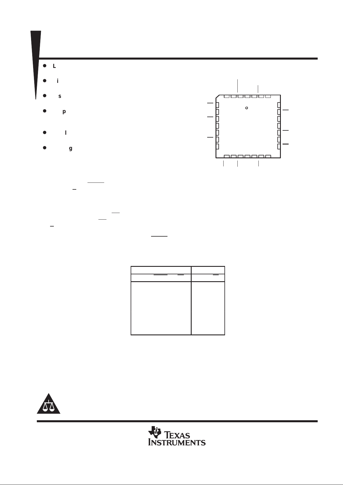
4
15 16 17 18
Y5
Y4
V
Y4Y3Y3
NCVCLKIN
V
28 27 26
25
24
23
22
21
20
19
12
Y5
CLKINOEGND
CC
CC0
REF
FN PACKAGE
(TOP VIEW)
NC – No internal connection
Page 2

CDC111
1-LINE TO 9-LINE DIFFERENTIAL LVPECL CLOCK DRIVER
SCAS321G – SEPTEMBER 1993 – REVISED AUGUST 1999
2
POST OFFICE BOX 655303 • DALLAS, TEXAS 75265
logic diagram (positive logic)
Y0
Y0
25
24
Y1
Y1
23
21
Y2
Y2
20
19
Y3
Y3
18
17
Y4
Y4
16
14
Y5
Y5
13
12
Y6
Y6
11
10
Y7
Y7
9
7
Y8
Y8
6
5
28
2
27
CLKIN
CLKIN
OE
absolute maximum ratings over operating free-air temperature range (unless otherwise noted)
†
Supply voltage range, VCC –0.5 V to 4.6 V. . . . . . . . . . . . . . . . . . . . . . . . . . . . . . . . . . . . . . . . . . . . . . . . . . . . . . . . .
Input voltage range, VI (see Note 1) –0.5 V to VCC + 0.5 V. . . . . . . . . . . . . . . . . . . . . . . . . . . . . . . . . . . . . . . . . .
Output voltage range, VO (see Note 1) –0.5 V to VCC + 0.5 V. . . . . . . . . . . . . . . . . . . . . . . . . . . . . . . . . . . . . . .
Input clamp current, IIK (VI < 0) –18 mA. . . . . . . . . . . . . . . . . . . . . . . . . . . . . . . . . . . . . . . . . . . . . . . . . . . . . . . . . . .
Output clamp current, I
OK
(VO < 0 or VO > VCC) –18 mA. . . . . . . . . . . . . . . . . . . . . . . . . . . . . . . . . . . . . . . . . . . .
Continuous output current, IO (VO = 0 to VCC) –50 mA. . . . . . . . . . . . . . . . . . . . . . . . . . . . . . . . . . . . . . . . . . . . . .
Continuous current through VCC or GND
"
80 mA. . . . . . . . . . . . . . . . . . . . . . . . . . . . . . . . . . . . . . . . . . . . . . . . . .
Maximum power dissipation at TA = 55°C (in still air) (see Note 2) 525 mW. . . . . . . . . . . . . . . . . . . . . . . . . . . . .
Storage temperature range, T
stg
–65°C to 150°C. . . . . . . . . . . . . . . . . . . . . . . . . . . . . . . . . . . . . . . . . . . . . . . . . . .
†
Stresses beyond those listed under “absolute maximum ratings” may cause permanent damage to the device. These are stress ratings only, and
functional operation of the device at these or any other conditions beyond those indicated under “recommended operating conditions” is not
implied. Exposure to absolute-maximum-rated conditions for extended periods may affect device reliability.
NOTES: 1. The input and output negative-voltage ratings may be exceeded if the input and output clamp-current ratings are observed.
2. The maximum package power dissipation is calculated using a juction temperature of 150_C and a board trace length of 750 mils.
For more information, refer to the
Package Thermal Considerations
application note in the
ABT Advanced BiCMOS T echnology Data
Book
, literature number SCBD002.
Page 3
CDC111
1-LINE TO 9-LINE DIFFERENTIAL LVPECL CLOCK DRIVER
SCAS321G – SEPTEMBER 1993 – REVISED AUGUST 1999
3
POST OFFICE BOX 655303 • DALLAS, TEXAS 75265
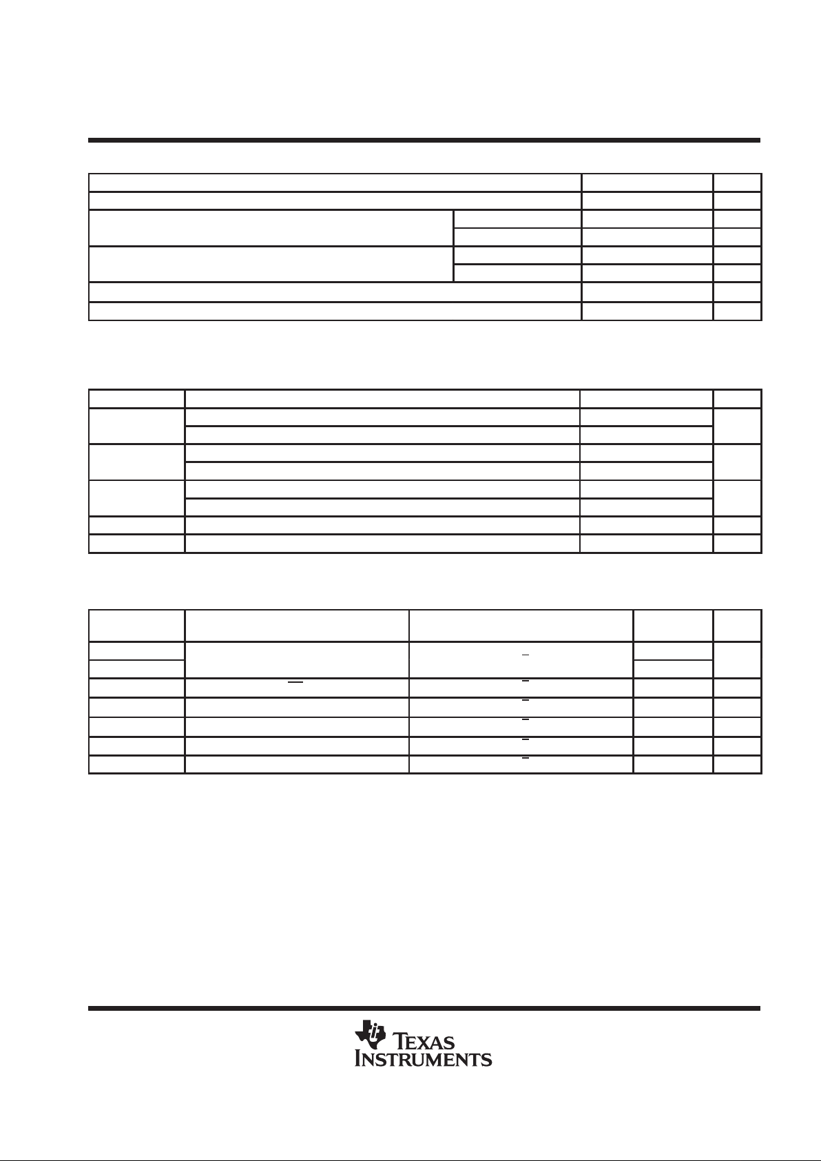
recommended operating conditions (see Note 3)
MIN MAX UNIT
V
CC
Supply voltage 3 3.6 V
p
VCC = 3 V to 3.6 V VCC–1.165 VCC–0.88 V
VIHHigh-level input voltage
VCC = 3.3 V 2.135 2.420 V
p
VCC = 3 V to 3.6 V VCC–1.81 VCC–1.475 V
VILLow-level input voltage
VCC = 3.3 V 1.49 1.825 V
T
A
Operating free-air temperature 0 70 °C
f
clock
Input frequency 500 MHz
NOTE 3: VCC = V
CCO
electrical characteristics over recommended operating free-air temperature range (unless
otherwise noted)
PARAMETER TEST CONDITIONS MIN MAX UNIT
VCC = 3 V to 3.6 V VCC–1.38 VCC–1.26
V
REF
VCC = 3.3 V 1.92 2.04
V
VCC = 3 V to 3.6 V VCC–1.025 VCC–0.88
V
OH
VCC = 3.3 V 2.275 2.42
V
VCC = 3 V to 3.6 V VCC–1.81 VCC–1.62
V
OL
VCC = 3.3 V 1.49 1.68
V
I
I
VI = 2.4 V, VCC = 3 .6 V 150 µA
I
CC
IO = 0, VCC = 3 .6 V 80 mA
switching characteristics over recommended operating free-air temperature range,
V
CC
= 3.3 V ± 0.3 V (see Figures 1 and 2)
FROM TO
PARAMETER
(INPUT) (OUTPUT)
MIN
MAX
UNIT
t
PLH
450 600
p
t
PHL
CLKIN, CLKIN
Y, Y
450 600
ps
t
PHL
OE
Y, Y 900 ps
t
sk(o)
Y, Y 50 ps
t
sk(pr)
Y, Y 150 ps
t
r
Y, Y 200 600 ps
t
f
Y, Y 200 600 ps
Page 4
CDC111
1-LINE TO 9-LINE DIFFERENTIAL LVPECL CLOCK DRIVER
SCAS321G – SEPTEMBER 1993 – REVISED AUGUST 1999
4
POST OFFICE BOX 655303 • DALLAS, TEXAS 75265
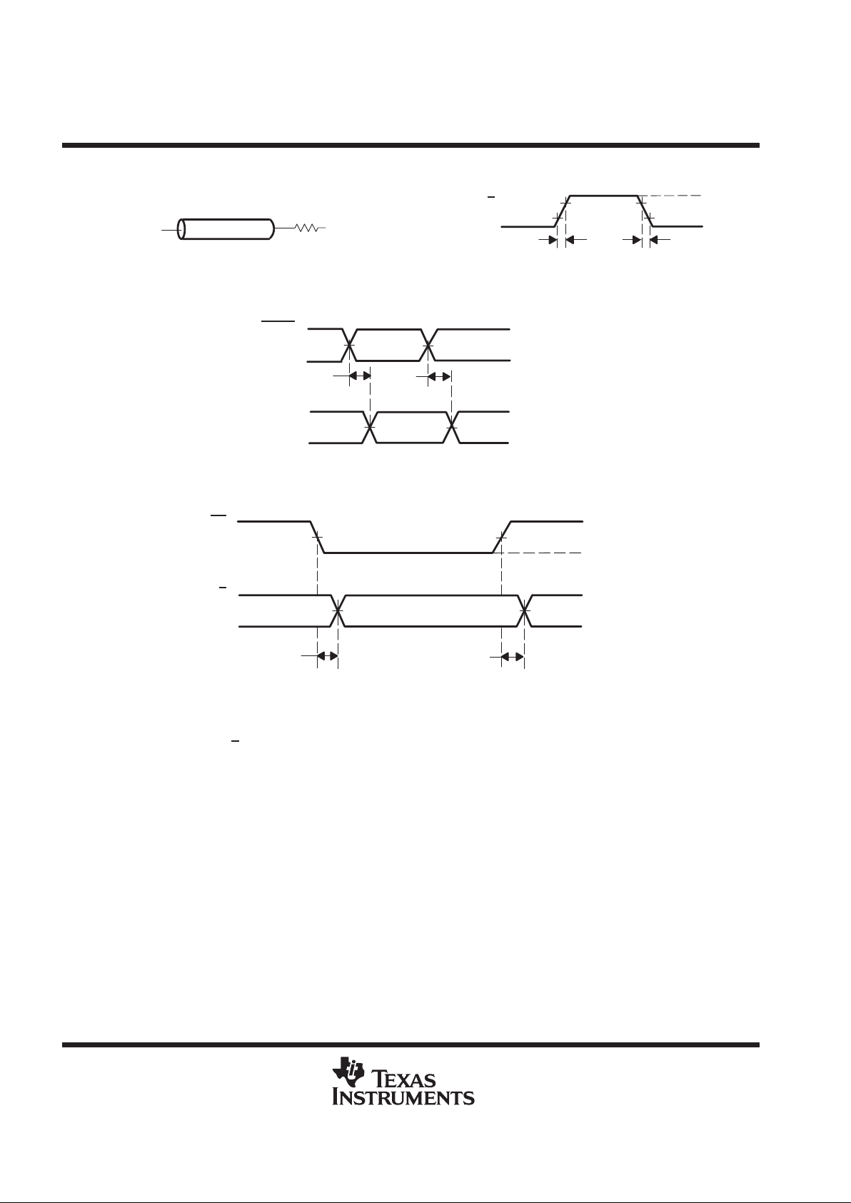
PARAMETER MEASUREMENT INFORMATION
From Output
Under Test
LOAD CIRCUIT
t
PLH
VCC – 0.9 V
VCC – 1.7 V
CLKIN
ZO = 50 Ω
50 Ω
V
OH
V
OL
VCC – 2 V
Y
Outputs
VOLTAGE WAVEFORMS
PROPAGATION DELAY TIMES
t
PLH
t
PHL
VCC – 0.9 V
VCC – 1.7 V
OE
V
OH
V
OL
Y
VOLTAGE WAVEFORMS
ENABLE AND DISABLE TIMES
Y
t
PLH
t
PHL
50%
t
PHL
50%
t
r
t
f
V
OH
V
OL
Y, Y
Outputs
80%
20%
80%
20%
VOLTAGE WAVEFORMS
RISE AND FALL TIMES
CLKIN
Waveform 1
NOTES: A. All input pulses are supplied by generators having the following characteristics: PRR ≤ 45 MHz, ZO = 50 Ω, tr ≤ 1 ns, tf≤ 1 ns.
B. Waveform 1 is for a Y
output with internal conditions such that the output is high except when disabled by the output control, and
for a Y output with internal conditions such that the output is low except when disabled by the output control.
C. The outputs are measured one at a time with one transition per measurement.
Figure 1. Load Circuit and Voltage Waveforms
Page 5

CDC111
1-LINE TO 9-LINE DIFFERENTIAL LVPECL CLOCK DRIVER
SCAS321G – SEPTEMBER 1993 – REVISED AUGUST 1999
5
POST OFFICE BOX 655303 • DALLAS, TEXAS 75265
PARAMETER MEASUREMENT INFORMATION
t
PLH1
t
PLH2
t
PLH3
t
PLH4
t
PHL4
t
PLH5
t
PLH6
t
PHL5
t
PHL6
t
PLH7
t
PHL7
t
PLH8
t
PHL8
t
PHL3
t
PHL2
t
PHL1
t
PLH9
t
PHL9
CLKIN
CLKIN
Y0
Y0
Y1
Y1
Y2
Y2
Y3
Y3
Y4
Y4
Y5
Y5
Y6
Y6
Y7
Y7
Y8
Y8
NOTES: A. Output skew, t
sk(o)
, is calculated as the greater of:
– The difference between the fastest and slowest t
PLHn
(n = 1, 2,...9)
– The difference between the fastest and slowest t
PHLn
(n = 1, 2
,...9)
B. Process skew, t
sk(pr)
, is calculated as the greater of:
– The difference between the fastest and slowest t
PLHn
(n = 1, 2,...9)
– The difference between the fastest and slowest t
PHLn
(n = 1, 2, . .. 9) across multiple devices
Figure 2. Waveforms for Calculation of t
sk(o)
, t
sk(pr)
Page 6

CDC111
1-LINE TO 9-LINE DIFFERENTIAL LVPECL CLOCK DRIVER
SCAS321G – SEPTEMBER 1993 – REVISED AUGUST 1999
6
POST OFFICE BOX 655303 • DALLAS, TEXAS 75265
MECHANICAL DATA
FN (S-PQCC-J**) PLASTIC J-LEADED CHIP CARRIER
4040005/B 03/95
20 PIN SHOWN
0.026 (0,66)
0.032 (0,81)
D2/E2
0.020 (0,51) MIN
0.180 (4,57) MAX
0.120 (3,05)
0.090 (2,29)
D2/E2
0.013 (0,33)
0.021 (0,53)
Seating Plane
MAX
D2/E2
0.219 (5,56)
0.169 (4,29)
0.319 (8,10)
0.469 (11,91)
0.569 (14,45)
0.369 (9,37)
MAX
0.356 (9,04)
0.456 (11,58)
0.656 (16,66)
0.008 (0,20) NOM
1.158 (29,41)
0.958 (24,33)
0.756 (19,20)
0.191 (4,85)
0.141 (3,58)
MIN
0.441 (11,20)
0.541 (13,74)
0.291 (7,39)
0.341 (8,66)
18
19
14
13
D
D1
13
9
E1E
4
8
MINMAXMIN
PINS
**
20
28
44
0.385 (9,78)
0.485 (12,32)
0.685 (17,40)
52
68
84
1.185 (30,10)
0.985 (25,02)
0.785 (19,94)
D/E
0.395 (10,03)
0.495 (12,57)
1.195 (30,35)
0.995 (25,27)
0.695 (17,65)
0.795 (20,19)
NO. OF
D1/E1
0.350 (8,89)
0.450 (11,43)
1.150 (29,21)
0.950 (24,13)
0.650 (16,51)
0.750 (19,05)
0.004 (0,10)
M
0.007 (0,18)
0.050 (1,27)
NOTES: A. All linear dimensions are in inches (millimeters).
B. This drawing is subject to change without notice.
C. Falls within JEDEC MS-018
Page 7

IMPORTANT NOTICE
T exas Instruments and its subsidiaries (TI) reserve the right to make changes to their products or to discontinue
any product or service without notice, and advise customers to obtain the latest version of relevant information
to verify, before placing orders, that information being relied on is current and complete. All products are sold
subject to the terms and conditions of sale supplied at the time of order acknowledgement, including those
pertaining to warranty, patent infringement, and limitation of liability.
TI warrants performance of its semiconductor products to the specifications applicable at the time of sale in
accordance with TI’s standard warranty. Testing and other quality control techniques are utilized to the extent
TI deems necessary to support this warranty. Specific testing of all parameters of each device is not necessarily
performed, except those mandated by government requirements.
CERT AIN APPLICATIONS USING SEMICONDUCTOR PRODUCTS MAY INVOLVE POTENTIAL RISKS OF
DEATH, PERSONAL INJURY, OR SEVERE PROPERTY OR ENVIRONMENTAL DAMAGE (“CRITICAL
APPLICATIONS”). TI SEMICONDUCTOR PRODUCTS ARE NOT DESIGNED, AUTHORIZED, OR
WARRANTED TO BE SUITABLE FOR USE IN LIFE-SUPPORT DEVICES OR SYSTEMS OR OTHER
CRITICAL APPLICATIONS. INCLUSION OF TI PRODUCTS IN SUCH APPLICA TIONS IS UNDERSTOOD T O
BE FULLY AT THE CUSTOMER’S RISK.
In order to minimize risks associated with the customer’s applications, adequate design and operating
safeguards must be provided by the customer to minimize inherent or procedural hazards.
TI assumes no liability for applications assistance or customer product design. TI does not warrant or represent
that any license, either express or implied, is granted under any patent right, copyright, mask work right, or other
intellectual property right of TI covering or relating to any combination, machine, or process in which such
semiconductor products or services might be or are used. TI’s publication of information regarding any third
party’s products or services does not constitute TI’s approval, warranty or endorsement thereof.
Copyright 1999, Texas Instruments Incorporated
 Loading...