

Page 1
July 1998
CD54AC541F3A,
SEMICONDUCTOR
CD54ACT541F3A
Octal Buffer/Line Driver
Three-State, Non-Inverting
Features
• This Circuit is Processed in Accordance to MIL-STD883 and is Fully Conformant Under the Provisions of
Paragraph 1.2.1.
• Exceeds 2kV ESD Protection MIL-STD-883, Method 3015
• Meets JEDEC Standard No. 20
• SCR - Latch-Up-Resistant CMOS Process and Circuit
Design
• Speed of Bipolar FAST/A/S with Significantly Reduced
Power Consumption
• Functionally and Pin-Compatible with Industry 54
Bipolar Types in the FAST, AS and S Series
• Balanced Propagation Delays
• Military Operating Temperature Range
- Ceramic (CERDIP) 54 Series: . . . . . . . . -55 to 125
o
• ±24mA Output Drive Current, Drives 75Ω Lines without Need for Terminations
• Fan Out (Over Temperature)
- ACL Loads . . . . . . . . . . . . . . . . . . . . . . . . . . . . . . 2400
- FAST Loads. . . . . . . . . . . . . . . . . . . . . . . . . . . . . . . . 15
- AS Loads. . . . . . . . . . . . . . . . . . . . . . . . . . . . . . . . . . 48
• Operating Voltage
- AC Types. . . . . . . . . . . . . . . . . . . . . . . . . .1.5V to 5.5V
- ACT Types. . . . . . . . . . . . . . . . . . . . . . . . . 4.5V to 5.5V
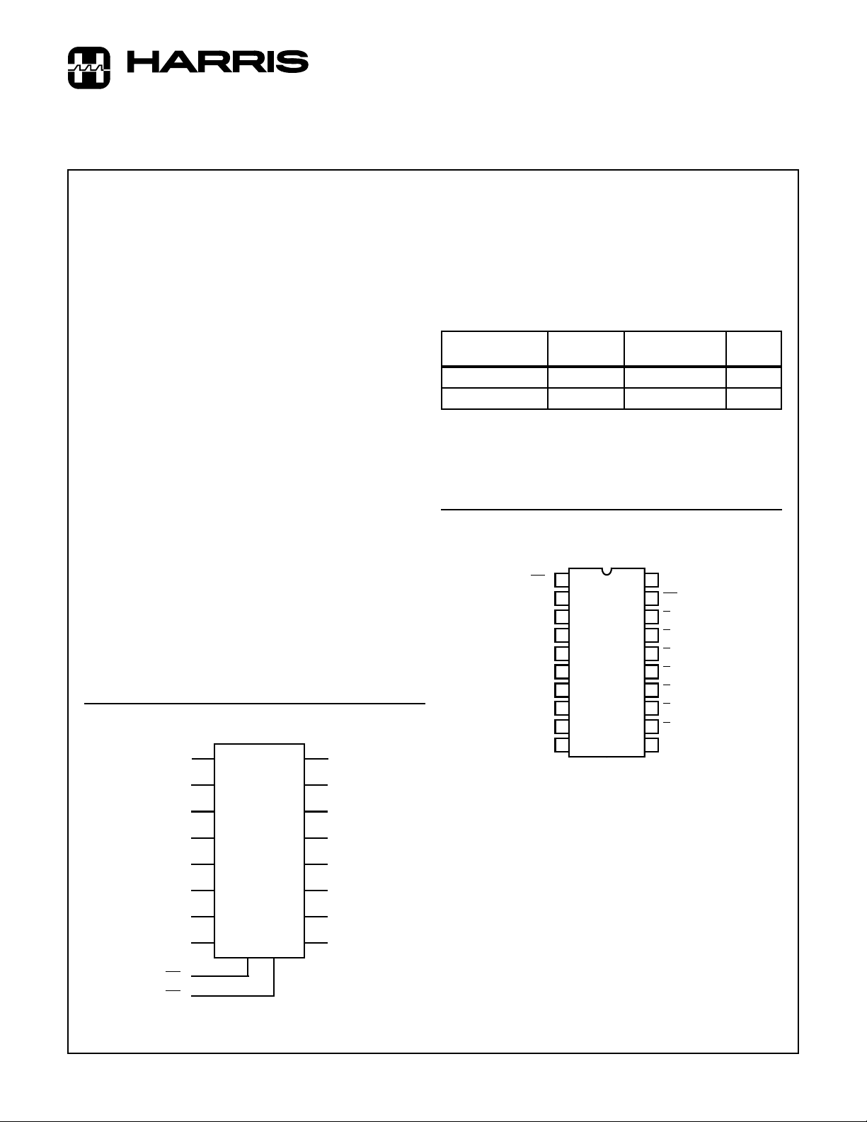
Functional Diagram
A0
A1
A2
A3
A4
A5
A6
A7
2
3
4
5
6
7
8
9
18
Y0
17
Y1
16
Y2
15
Y3
14
Y4
13
Y5
12
Y6
11
Y7
Description
The CD54AC541F3A and CD54ACT541F3A are octal
buffer/line drivers that utilize the Harris Advanced CMOS
Logic technology. The CD54AC541F3A and
CD54ACT541F3A are non-inverting three-state buffershaving
two active-LOW output enab les.
Ordering Information
TEMP.
PART NUMBER
CD54AC541F3A -55 to 125 20 Ld CERDIP F20.3
CD54ACT541F3A -55 to 125 20 Ld CERDIP F20.3
NOTE:
1. Waf erand die forthis part number is availablewhich meets all electrical specifications. Please contact your local sales office or Harris
customer service for ordering information.
RANGE (oC) PACKAGE
C
Pinout
OE
A0
A1
A2
A3
A4
A5
A6
A7
GND
1
1
2
3
4
5
6
7
8
9
10
V
20
CC
OE
19
2
Y0
18
Y1
17
Y2
16
Y3
15
Y4
14
Y5
13
12
Y6
Y7
11
PKG.
NO.
OE
1
OE
2
CAUTION: These devices are sensitive to electrostatic discharge. Users should follow proper IC Handling Procedures.
Copyright
© Harris Corporation 1998
1
19
GND = 10
V
= 20
CC
1
File Number 3914.1
Page 2
CD54AC541F3A, CD54ACT541F3A
Absolute Maximum Ratings Thermal Information
DC Supply Voltage, VCC. . . . . . . . . . . . . . . . . . . . . . . . -0.5V to 6V
DC Input Diode Current, I
IK
For VI < -0.5V or VI > VCC + 0.5V. . . . . . . . . . . . . . . . . . . . . .±20mA
DC Output Diode Current, I
OK
For VO < -0.5V or VO > VCC + 0.5V . . . . . . . . . . . . . . . . . . . .±50mA
DC Output Source or Sink Current per Output Pin, I
O
For VO > -0.5V or VO < VCC + 0.5V . . . . . . . . . . . . . . . . . . . .±50mA
DC VCC or Ground Current, I
CC orIGND
(Note 2) . . . . . . . . .±100mA
Operating Conditions
Temperature Range, TA . . . . . . . . . . . . . . . . . . . . . . -55oC to 125oC
Supply Voltage Range, VCC (Note 3)
AC Types. . . . . . . . . . . . . . . . . . . . . . . . . . . . . . . . . . .1.5V to 5.5V
ACT Types . . . . . . . . . . . . . . . . . . . . . . . . . . . . . . . . .4.5V to 5.5V
DC Input or Output Voltage, VI, VO . . . . . . . . . . . . . . . . . 0V to V
Input Rise and Fall Slew Rate, dt/dv
AC Types
1.5V to 3V. . . . . . . . . . . . . . . . . . . . . . . . . . . . . . . . . . 50ns (Max)
3.6V to 5.5V . . . . . . . . . . . . . . . . . . . . . . . . . . . . . . . . 20ns (Max)
4.5V to 5.5V . . . . . . . . . . . . . . . . . . . . . . . . . . . . . . . . 10ns (Max)
CAUTION: Stresses above those listed in “Absolute Maximum Ratings” may cause permanent damage to the device. This is a stress only rating and operation
of the device at these or any other conditions above those indicated in the operational sections of this specification is not implied.
NOTES:
2. For up to 4 outputs per device, add ±25mA for each additional output.
3. Unless otherwise specified, all voltages are referenced to ground.
4. θJA is measured with the component mounted on an evaluation PC board in free air.
Thermal Resistance (Typical, Note 4) θJA (oC/W) θJC (oC/W)
CERDIP Package . . . . . . . . . . . . . . . . 85 24
Maximum Junction Temperature (Hermetic P ac kage or Die) . . . 175oC
Maximum Storage Temperature Range . . . . . . . . . .-65oC to 150oC
Maximum Lead Temperature (Soldering 10s). . . . . . . . . . . . . 300oC
CC
DC Electrical Specifications
PARAMETER SYMBOL
AC TYPES
High Level Input Voltage V
Low Level Input Voltage V
High Level Output Voltage V
IH
IL
OH
TEST
CONDITIONS
(V) IO(mA) MIN MAX MIN MAX
I
V
CC
(V)
o
C -55oC TO 125oC
25
- - 1.5 1.2 - 1.2 - V
3 2.1 - 2.1 - V
4.5 3.15
(Note 5)
- 3.15
(Note 5)
-V
5.5 3.85 - 3.85 - V
- - 1.5 - 0.3 - 0.3 V
3 - 0.9 - 0.9 V
4.5 - 1.35
(Note 5)
- 1.35
(Note 5)
5.5 - 1.65 - 1.65 V
VIH or V
-0.05 1.5 1.4 - 1.4 - V
IL
-0.05 3 2.9 - 2.9 - V
-0.05 4.5 4.4 - 4.4 - V
-4 3 2.58 - 2.4 - V
-24 4.5 3.94
(Note 5)
-50
5.5 - - 3.85 - V
- 3.7
(Note 5)
-V
(Note 6, 7)
UNITSV
V
2
Page 3

CD54AC541F3A, CD54ACT541F3A
DC Electrical Specifications (Continued)
TEST
PARAMETER SYMBOL
Low Level Output Voltage V
OL
CONDITIONS
(V) IO(mA) MIN MAX MIN MAX
I
VIH or V
0.05 1.5 - 0.1 - 0.1 V
IL
V
CC
(V)
0.05 3 - 0.1 - 0.1 V
0.05 4.5 - 0.1 - 0.1 V
12 3 - 0.36 - 0.5 V
24 4.5 - 0.36
50
5.5 - - - 1.65 V
(Note 6, 7)
Input Leakage Current I
I
VCC or
- 5.5 - ±0.1
GND
Three-State Leakage
Current
I
OZ
VIH or V
VO = V
CC
IL
- 5.5 - ±0.5
or GND
Quiescent Device Current I
CC
VCC or
0 5.5 - 8
GND
ACT TYPES
High Level Input Voltage V
IH
- - 4.5 to 5.5 2
(Note 5)
Low Level Input Voltage V
High Level Output Voltage V
IL
OH
- - 4.5 to 5.5 - 0.8
VIH or V
-0.05 4.5 4.4 - 4.4 - V
IL
-24 4.5 3.94
(Note 5)
-50
5.5 - - 3.85 - V
(Note 6, 7)
Low Level Output Voltage V
OL
VIH or V
0.05 4.5 - 0.1 - 0.1 V
IL
24 4.5 - 0.36
50
5.5 - - - 1.65 V
(Note 6, 7)
Input Leakage Current I
I
VCC or
- 5.5 - ±0.1
GND
Three-State or Leakage
Current
I
OZ
VIH or V
VO = V
CC
IL
- 5.5 - ±0.5
or GND
Quiescent Device Current I
CC
VCC or
0 5.5 - 8
GND
AdditionalSupply Current per
Input Pin TTL Inputs High
∆I
CC
V
CC
- 4.5 to 5.5 - 2.4 - 3 mA
-2.1
1 Unit Load
NOTES:
5. Tested 100%.
6. Test one output at a time for a 1-second maximum duration. Measurement is made by forcing current and measuring voltage to minimize
power dissipation.
7. Test verifies a minimum transmission-line-drive capability of 75Ω for 54AC/ACT Series.
o
C -55oC TO 125oC
25
- 0.5
(Note 5)
- ±1
(Note 5)
- ±10
(Note 5)
- 160
(Note 5)
-2
(Note 5)
- 0.8
(Note 5)
- 3.7
(Note 5)
- 0.5
(Note 5)
- ±1
(Note 5)
- ±10
(Note 5)
- 160
(Note 5)
UNITSV
V
(Note 5)
µA
(Note 5)
µA
(Note 5)
µA
(Note 5)
-V
V
(Note 5)
-V
V
(Note 5)
µA
(Note 5)
µA
(Note 5)
µA
(Note 5)
3
Page 4

CD54AC541F3A, CD54ACT541F3A
ACT Input Load Table
INPUT UNIT LOAD
Data 0.5
OE1, OE2 1.3
NOTE: Unit load is ∆ICClimit specified in DC Electrical Specifications
Table, e .g., 2.4mA max at 25oC.
Switching Specifications Input t
, tf = 3ns, CL= 50pF (Worst Case)
r
-55oC TO 125oC
PARAMETER SYMBOL VCC (V)
AC TYPES
Propagation Delay, Data to Output t
PLH
, t
PHL
1.5 - - 98 ns
3.3 (Note 9) 3.3 - 10.9 ns
5 (Note 10) 2.3 - 7.8 (Note 8) ns
Propagation Delay, Enable, Disable to
Output
t
PZL
, t
PZH
1.5 - - 150
3.3 5.4 - 18
5 3.6 - 12 (Note 8)
t
PLZ
, t
PHZ
1.5 - - 150
3.3 4.5 - 15
5 3.6 - 12 (Note 8)
Minimum (Valley) VOH During Switching
of Other Outputs
V
OHV
See Figure 1
5 - 4 at 25oC- V
(Output Under Test Not Switching)
Maximum (Peak) VOLDuring Switching of
Other Outputs
V
OLP
See Figure 1
5 - 1 at 25oC- V
(Output Under Test Not Switching)
Three-State Output Capacitance C
Input Capacitance C
O
I
---15pF
---10pF
Power Dissipation Capacitance CPD (Note 11) - - 60 - pF
ACT TYPES
Propagation Delay, Data to Output t
Propagation Delay, Enable, Disable to
Output
Minimum (Valley) VOH During Switching
of Other Outputs
, t
PLH
PHL
t
, t
PLZ
PZL
t
, t
PZH
PHZ
V
OHV
See Figure 1
5 (Note 10) 2.5 - 8.3 (Note 8) ns
,
5 4 - 13.4 (Note 8) ns
5 - 4 at 25oC- V
(Output Under Test Not Switching)
Maximum (Peak) VOLDuring Switching of
Other Outputs
V
OLP
See Figure 1
5 - 1 at 25oC- V
(Output Under Test Not Switching)
Three-State Output Capacitance C
Input Capacitance C
O
I
---15pF
---10pF
Power Dissipation Capacitance CPD (Note 11) - - 60 - pF
NOTES:
8. Limits tested 100%.
9. 3.3V Min is at 3.6V, Max si at 3V.
10. 5V Min is at 5.5V, Max is at 4.5V
11. CPD is used to determine the dynamic power consumption per gate.
AC: PD = V
ACT: PD = V
2
fi(CPD + CL)
CC
2
fi(CPD + CL) + VCC∆ICC where fi = input frequency, CL = output load capacitance, VCC = supply voltage.
CC
UNITSMIN TYP MAX
4
Page 5

CD54AC541F3A, CD54ACT541F3A
Burn-In Test Circuit Connections (Use DC II for F3A Burn-In and AC for Life Test)
DC BURN-IN I DC BURN-IN II
DC
OPEN GROUND V
CD54AC/ACT541 11-18 1-10, 19 20 11-18 10 1-9, 19, 20
AC OPEN GROUND 1/2 VCC (3V) VCC (6V)
CD54AC/ACT541 - 10 11-18 20 1, 19 2-9
NOTE: Each pin except VCC and Gnd will have a resistor of 2kΩ-47kΩ.
OUTPUT
R
(NOTE)
L
DUT
500Ω
(6V) OPEN GROUND VCC (6V)
CC
OSCILLATOR
50kHz 25kHz
OUTPUT
LOAD
C
L
50pF
NOTE: For AC Series Only: When VCC = 1.5V, RL = 1kΩ.
CD54AC CD54ACT
Input Level V
Input Switching Voltage, V
Output Switching Voltage, V
S
S
0.5 V
0.5 V
CC
CC
CC
3V
1.5V
0.5 V
CC
FIGURE 1. PROPAGATION DELAY TIMES
All Harris Semiconductor products are manufactured, assembled and tested under ISO9000 quality systems certification.
Harris Semiconductor products are sold by description only. Harris Semiconductor reserves the right to make changes in circuit design and/or specifications at
any time without notice. Accordingly, the reader is cautioned to verify that data sheets are current before placing orders. Information furnished by Harris is
believed to be accurate and reliable. However, no responsibility is assumed by Harris or its subsidiaries for its use; nor for any infringements of patents or other
rights of third parties which may result from its use. No license is granted by implication or otherwise under any patent or patent rights of Harris or its subsidiaries.
Sales Office Headquarters
For general information regarding Harris Semiconductor and its products, call 1-800-4-HARRIS
NORTH AMERICA
Harris Semiconductor
P. O. Box 883, Mail Stop 53-210
Melbourne, FL 32902
TEL: 1-800-442-7747
(407) 729-4984
FAX: (407) 729-5321
EUROPE
Harris Semiconductor
Mercure Center
100, Rue de la Fusee
1130 Brussels, Belgium
TEL: (32) 2.724.2111
FAX: (32) 2.724.22.05
SEMICONDUCTOR
5
ASIA
Harris Semiconductor PTE Ltd.
No. 1 Tannery Road
Cencon 1, #09-01
Singapore 1334
TEL: (65) 748-4200
FAX: (65) 748-0400
 Loading...