

Page 1
Semiconductor
CD54AC00F3A,
CD54ACT00F3A
July 1998
Features
• This Circuit is Processed in Accordance to MIL-STD883 and is Fully Conformant Under the Provisions of
Paragraph 1.2.1.
• Exceeds 2kV ESD Protection MIL-STD-883, Method 3015
• Meets JEDEC Standard No. 20
• SCR - Latch-Up-Resistant CMOS Process and Circuit
Design
• Speed of Bipolar FAST/A/S with Significantly Reduced
Power Consumption
• Functionally and Pin-Compatible with Industry 54
Bipolar Types in the FAST, AS and S Series
• Balanced Propagation Delays
• Military Operating Temperature Range
- Ceramic (CERDIP) 54 Series: . . . . . . . . -55 to 125
• ±24mA Output Drive Current, Drives 75Ω Lines without Need for Terminations
• Fan Out (Over Temperature)
- ACL Loads . . . . . . . . . . . . . . . . . . . . . . . . . . . . . . 2400
- FAST Loads. . . . . . . . . . . . . . . . . . . . . . . . . . . . . . . . 15
- AS Loads. . . . . . . . . . . . . . . . . . . . . . . . . . . . . . . . . . 48
• Balanced Noise Immunity at 30% of Supply for AC
Types
• Supply Voltage Range
- AC Types. . . . . . . . . . . . . . . . . . . . . . . . . .1.5V to 5.5V
- ACT Types. . . . . . . . . . . . . . . . . . . . . . . . . 4.5V to 5.5V
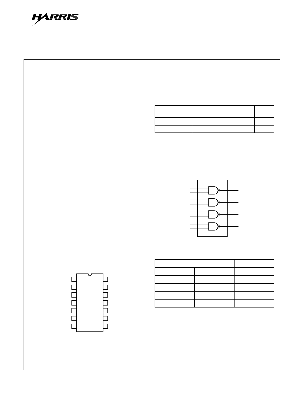
Pinout
1A
1B
1Y
2A
2B
2Y
GND
1
2
3
4
5
6
7
14
V
CC
4A
13
12
4B
11
4Y
10
3A
9
3B
8
3Y
Quad 2-Input NAND Gate
Description
The CD54AC00F3A and CD54ACT00F3A are quad 2-input
NAND gates that utilize the Harris Advanced CMOS Logic
technology.
Ordering Information
TEMP.
PART NUMBER
CD54AC00F3A -55 to 125 14 Ld CERDIP F14.3
CD54ACT00F3A -55 to 125 14 Ld CERDIP F14.3
NOTE:
1. Wafer and die for this part number is available which meets all electrical specifications. Please contact your local sales office or Harris
customer service for ordering information.
o
Functional Diagram
C
ABY
LLH
HLH
LHH
HHL
RANGE (oC) PACKAGE
1
1A
2
1B
4
2A
5
2B
9
3B
10
3A
12
4B
13
4A
TRUTH TABLE
INPUTS OUTPUTS
3
6
8
11
GND = 7
V
CC
1Y
2Y
3Y
4Y
= 14
PKG.
NO.
CAUTION: These devices are sensitive to electrostatic discharge. Users should follow proper IC Handling Procedures.
Copyright
© Harris Corporation 1998
1
File Number 3876.1
Page 2
CD54AC00F3A, CD54ACT00F3A
Absolute Maximum Ratings Thermal Information
DC Supply Voltage, VCC. . . . . . . . . . . . . . . . . . . . . . . . -0.5V to 6V
DC Input Diode Current, I
IK
For VI < -0.5V or VI > VCC + 0.5V. . . . . . . . . . . . . . . . . . . . . .±20mA
DC Output Diode Current, I
OK
For VO < -0.5V or VO > VCC + 0.5V . . . . . . . . . . . . . . . . . . . .±50mA
DC Output Source or Sink Current per Output Pin, I
O
For VO > -0.5V or VO < VCC + 0.5V . . . . . . . . . . . . . . . . . . . .±50mA
DC VCC or Ground Current, I
CC orIGND
(Note 2) . . . . . . . . .±100mA
Operating Conditions
Temperature Range, TA . . . . . . . . . . . . . . . . . . . . . . -55oC to 125oC
Supply Voltage Range, VCC (Note 3)
AC Types. . . . . . . . . . . . . . . . . . . . . . . . . . . . . . . . . . .1.5V to 5.5V
ACT Types . . . . . . . . . . . . . . . . . . . . . . . . . . . . . . . . .4.5V to 5.5V
DC Input or Output Voltage, VI, VO . . . . . . . . . . . . . . . . . 0V to V
Input Rise and Fall Slew Rate, dt/dv
AC Types
1.5V to 3V. . . . . . . . . . . . . . . . . . . . . . . . . . . . . . . . . . 50ns (Max)
3.6V to 5.5V . . . . . . . . . . . . . . . . . . . . . . . . . . . . . . . . 20ns (Max)
4.5V to 5.5V . . . . . . . . . . . . . . . . . . . . . . . . . . . . . . . . 10ns (Max)
CAUTION: Stresses above those listed in “Absolute Maximum Ratings” may cause permanent damage to the device. This is a stress only rating and operation
of the device at these or any other conditions above those indicated in the operational sections of this specification is not implied.
NOTES:
2. For up to 4 outputs per device, add ±25mA for each additional output.
3. Unless otherwise specified, all voltages are referenced to ground.
4. θJA is measured with the component mounted on an evaluation PC board in free air.
Thermal Resistance (Typical, Note 4) θJA (oC/W) θJC (oC/W)
CERDIP Package . . . . . . . . . . . . . . . . 80 24
Maximum Junction Temperature (Hermetic P ac kage or Die) . . . 175oC
Maximum Storage Temperature Range . . . . . . . . . .-65oC to 150oC
Maximum Lead Temperature (Soldering 10s). . . . . . . . . . . . . 300oC
CC
DC Electrical Specifications
PARAMETER SYMBOL
AC TYPES
High Level Input Voltage V
Low Level Input Voltage V
High Level Output Voltage V
IH
IL
OH
TEST
CONDITIONS
(V) IO(mA) MIN MAX MIN MAX
I
V
CC
(V)
o
25
C -55oC TO 125oC
- - 1.5 1.2 - 1.2 - V
3 2.1 - 2.1 - V
4.5 3.15
(Note 5)
- 3.15
(Note 5)
-V
5.5 3.85 - 3.85 - V
- - 1.5 - 0.3 - 0.3 V
3 - 0.9 - 0.9 V
4.5 - 1.35
(Note 5)
- 1.35
(Note 5)
5.5 - 1.65 - 1.65 V
VIH or V
-0.05 1.5 1.4 - 1.4 - V
IL
-0.05 3 2.9 - 2.9 - V
-0.05 4.5 4.4 - 4.4 - V
-4 3 2.58 - 2.4 - V
-24 4.5 3.94
(Note 5)
-50
5.5 - - 3.85 - V
- 3.7
(Note 5)
-V
(Note 6, 7)
UNITSV
V
2
Page 3

CD54AC00F3A, CD54ACT00F3A
DC Electrical Specifications (Continued)
TEST
PARAMETER SYMBOL
Low Level Output Voltage V
OL
CONDITIONS
(V) IO(mA) MIN MAX MIN MAX
I
VIH or V
0.05 1.5 - 0.1 - 0.1 V
IL
V
CC
(V)
0.05 3 - 0.1 - 0.1 V
0.05 4.5 - 0.1 - 0.1 V
12 3 - 0.36 - 0.5 V
24 4.5 - 0.36
50
5.5 - - - 1.65 V
(Note 6, 7)
Input Leakage Current I
I
VCC or
- 5.5 - ±0.1
GND
Quiescent Device Current I
CC
0 5.5 - 4
ACT TYPES
High Level Input Voltage V
IH
- - 4.5 to 5.5 2
(Note 5)
Low Level Input Voltage V
High Level Output Voltage V
IL
OH
- - 4.5 to 5.5 - 0.8
VIH or V
-0.05 4.5 4.4 - 4.4 - V
IL
-24 4.5 3.94
(Note 5)
-50
5.5 - - 3.85 - V
(Note 6, 7)
Low Level Output Voltage V
OL
VIH or V
0.05 4.5 - 0.1 - 0.1 V
IL
24 4.5 - 0.36
50
5.5 - - - 1.65 V
(Note 6, 7)
Input Leakage Current I
I
VCC or
- 5.5 - ±0.1
GND
Quiescent Device Current I
CC
VCC or
0 5.5 - 4
GND
AdditionalSupply Current per
Input Pin TTL Inputs High
∆I
CC
V
CC
-2.1
- 4.5 to 5.5 - 2.4 - 3 mA
1 Unit Load
NOTES:
5. Tested at 100%.
6. Test one output at a time for a 1-second maximum duration. Measurement is made by forcing current and measuring voltage to minimize
power dissipation.
7. Test verifies a minimum transmission-line-drive capability of 75Ω for 54AC/ACT Series.
o
25
C -55oC TO 125oC
- 0.5
(Note 5)
- ±1
(Note 5)
-80
(Note 5)
-2
(Note 5)
- 0.8
(Note 5)
- 3.7
(Note 5)
- 0.5
(Note 5)
- ±1
(Note 5)
-80
(Note 5)
UNITSV
V
(Note 5)
µA
(Note 5)
µA
(Note 5)
-V
V
(Note 5)
-V
V
(Note 5)
µA
(Note 5)
µA
(Note 5)
ACT Input Load Table
INPUT UNIT LOAD
All 0.15
NOTE: Unit load is ∆ICClimit specified in DC Electrical Specifications
Table, e .g., 2.4mA max at 25oC.
3
Page 4

CD54AC00F3A, CD54ACT00F3A
Switching Specifications Input t
, tf = 3ns, CL= 50pF (Worst Case)
r
-55oC TO 125oC
PARAMETER SYMBOL VCC (V)
AC TYPES
Propagation Delay, Input to Output t
PLH, tPHL
1.5 - - 91 ns
3.3 (Note 9) 3.1 - 10.2 ns
5 (Note 10) 2.2 - 7.3 (Note 8) ns
Input Capacitance C
I
---10pF
Power Dissipation Capacitance CPD (Note 11) - - 45 - pF
ACT TYPES
Propagation Delay, Input to Output t
PLH
t
PHL
Input Capacitance C
I
5 (Note 10) 3.2 - 10.8 (Note 8) ns
4 - 13.2 (Note 8) ns
---10pF
Power Dissipation Capacitance CPD (Note 11) - - 45 - pF
NOTES:
8. Limits tested at 100%.
9. 3.3V Min at 3.6V, Max at 3V.
10. 5V Min at 5.5V, Max at 4.5V
11. CPD is used to determine the dynamic power consumption per gate.
AC: PD = V
ACT: PD = V
2
fi(CPD + CL)
CC
2
fi(CPD + CL) + VCC∆ICC where fi = input frequency, CL = output load capacitance, VCC = supply voltage.
CC
UNITSMIN TYP MAX
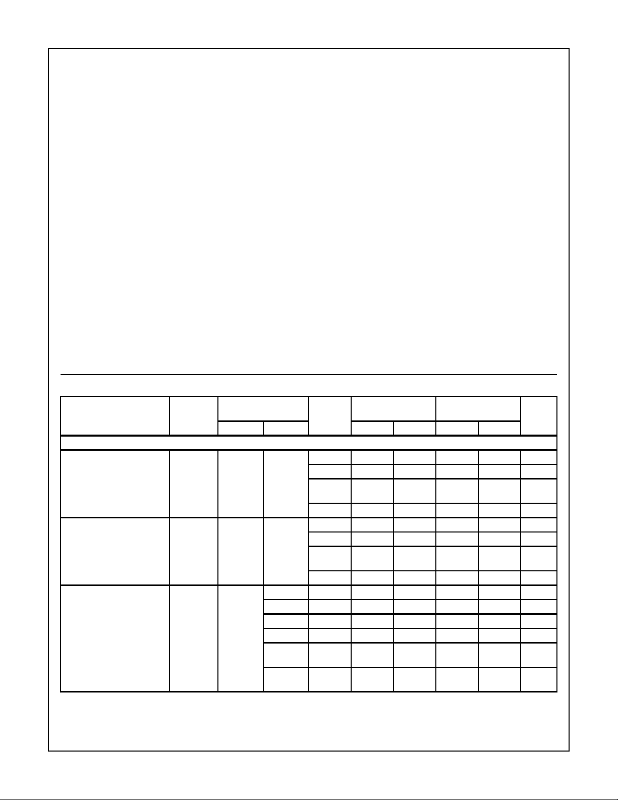
Burn-In Test Circuit Connections (Use DC II for F3A Burn-In and AC for Life Test)
DC BURN-IN I DC BURN-IN II
DC
CD54AC/ACT00 3, 6, 8, 11 1, 2, 4,5, 7, 9, 10,
AC OPEN GROUND 1/2 VCC (3V) VCC (6V)
CD54AC/ACT00 - 7 3, 6, 8, 11 14 1, 2, 4, 5, 9, 10,
NOTE: Each pin except VCC and Gnd will have a resistor of 2kΩ-47kΩ.
NOTE: For AC Series Only: When VCC = 1.5V, RL = 1kΩ.
Input Level V
Input Switching Voltage, V
Output Switching Voltage, V
FIGURE 1. PROPAGATION DELAY TIMES
OPEN GROUND VCC (6V) OPEN GROUND VCC (6V)
14 3, 6, 8, 11 7 1, 2, 4, 5, 9, 10,
12, 13
OSCILLATOR
50kHz 25kHz
12, 13
t
PLH
t
f
OUTPUT
DUT
OUTPUT
LOAD
R
L
C
L
50pF
(NOTE)
500Ω
tr = 3ns
LEVEL
V
I
V
O
INPUT
t
PHL
CD54AC CD54ACT
CC
S
S
0.5 V
0.5 V
CC
CC
3V
1.5V
0.5 V
CC
FIGURE 2. WAVEFORMS
= 3ns
12 - 14
90%
V
S
10%
V
S
-
GND
4
 Loading...