

Page 1
TL/F/6003
CD4723BM/CD4723BC Dual 4-Bit Addressable Latch
CD4724BM/CD4724BC 8-Bit Addressable Latch
February 1988
CD4723BM/CD4723BC Dual 4-Bit Addressable Latch
CD4724BM/CD4724BC 8-Bit Addressable Latch
General Description
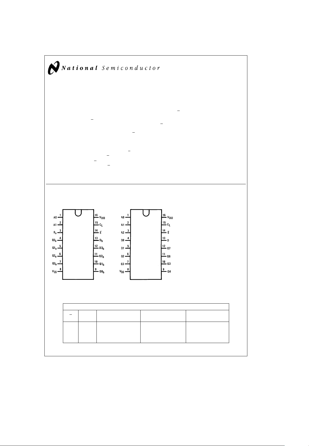
The CD4723B is a dual 4-bit addressable latch with common control inputs, including two address inputs (A0, A1),
an active low enable input (E
), and an active high clear input
(CL). Each latch has a data input (D) and four outputs (Q0 –
Q3). The CD4724B is an 8-bit addressable latch with three
address inputs (A0 –A2), an active low enable input (E
), active high clear input (CL), a data input (D) and eight outputs
(Q0–Q7).
Data is entered into a particular bit in the latch when that is
addressed by the address inputs and the enable (E
) is low.
Data entry is inhibited when enable (E
) is high.
When clear (CL) and enable (E) are high, all outputs are low.
When clear (CL) is high and enable (E
) is low, the channel
demultiplexing occurs. The bit that is addressed has an active output which follows the data input while all unaddressed bits are held low. When operating in the address-
able latch mode (E
eCLe
low), changing more than one
bit of the address could impose a transient wrong address.
Therefore, this should only be done while in the memory
mode (E
e
high, CLelow).
Features
Y
Wide supply voltage range 3.0V to 15V
Y
High noise immunity 0.45 VDD(typ.)
Y
Low power TTL fan out of 2 driving 74L
compatibility or 1 driving 74LS
Y
Serial to parallel capability
Y
Storage register capability
Y
Random (addressable) data entry
Y
Active high demultiplexing capability
Y
Common active high clear
Connection Diagrams
CD4723B
Dual-In-Line Package
TL/F/6003– 1
Top View
CD4724B
Dual-In-Line Package
TL/F/6003– 2
Top View
Order Number CD4723B or
CD4724B
Truth Table
Mode Selection
E CL
Addressed Unaddressed
Mode
Latch Latch
L L Follows Data Holds Previous Data Addressable Latch
H L Hold Previous Data Holds Previous Data Memory
L H Follows Data Reset to ‘‘0’’ Demultiplexer
H H Reset to ‘0’’ Reset to ‘‘0’’ Clear
C
1995 National Semiconductor Corporation RRD-B30M105/Printed in U. S. A.
Page 2
Absolute Maximum Ratings (Notes1&2)
If Military/Aerospace specified devices are required,
please contact the National Semiconductor Sales
Office/Distributors for availability and specifications.
DC Supply Voltage (V
DD
)
b
0.5V toa18 V
DC
Input Voltage (VIN)
b
0.5V to V
DD
a
0.5 V
DC
Storage Temperature (TS)
b
65§Ctoa150§C
Power Dissipation (PD)
Dual-In-Line 700 mW
Small Outline 500 mW
Lead Temperature (T
L
)
(Soldering, 10 seconds) 260
§
C
Recommended Operating
Conditions
(Note 2)
DC Supply Voltage (VDD) 3.0V to 15 V
DC
Input Voltage (VIN) 0VtoVDDV
DC
Operating Temperature Range (TA)
CD4723BM/CD4724BM
b
55§Ctoa125§C
CD4723BC/CD4724BC
b
40§Ctoa85§C
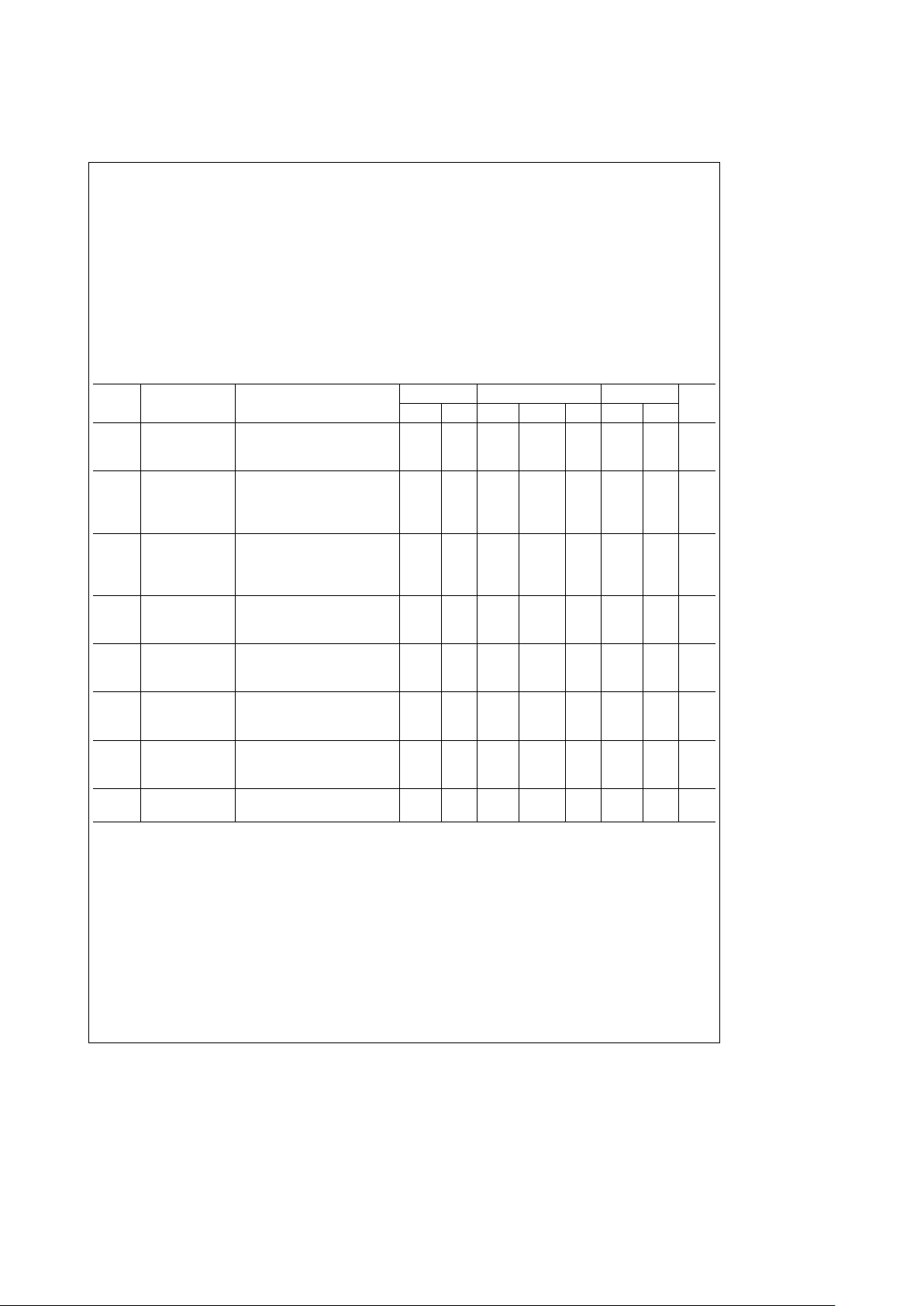
DC Electrical Characteristics CD4723BM/CD4724BM (Note 2)
Symbol Parameter Conditions
b
55§C
a
25§C
a
125§C
Units
Min Max Min Typ Max Min Max
I
DD
Quiescent Device V
DD
e
5V 5.0 0.02 5.0 150 m A
Current V
DD
e
10V 10 0.02 10 300 m A
V
DD
e
15V 20 0.02 20 600 m A
V
OL
Low Level
l
I
O
l
s
1 mA
Output Voltage V
DD
e
5V 0.05 0 0.05 0.05 V
V
DD
e
10V 0.05 0 0.05 0.05 V
V
DD
e
15V 0.05 0 0.05 0.05 V
V
OH
High Level
l
I
O
l
s
1 mA
Output Voltage V
DD
e
5V 4.95 4.95 5.0 4.95 V
V
DD
e
10V 9.95 9.95 10 9.95 V
V
DD
e
15V 14.95 14.95 15 14.95 V
V
IL
Low Level V
DD
e
5V, V
O
e
0.5V or 4.5V 1.5 2.25 1.5 1.5 V
Input Voltage V
DD
e
10V, V
O
e
1V or 9V 3.0 4.5 3.0 3.0 V
V
DD
e
15V, V
O
e
1.5V or 13.5V 4.0 6.75 4.0 4.0 V
V
IH
High Level V
DD
e
5V, V
O
e
0.5V or 4.5V 3.5 3.5 2.75 3.5 V
Input Voltage V
DD
e
10V, V
O
e
1V or 9V 7.0 7.0 5.5 7.0 V
V
DD
e
15V, V
O
e
1.5V or 13.5V 11.0 11.0 8.25 11.0 V
I
OL
Low Level Output V
DD
e
5V, V
O
e
0.4V 0.64 0.51 0.88 0.36 mA
Current V
DD
e
10V, V
O
e
0.5V 1.6 1.3 2.25 0.9 mA
(Note 3) V
DD
e
15V, V
O
e
1.5V 4.2 3.4 8.8 2.4 mA
I
OH
High Level Output V
DD
e
5V, V
O
e
4.6V
b
0.64
b
0.51b0.88
b
0.36 mA
Current V
DD
e
10V, V
O
e
9.5V
b
1.6
b
1.3b2.25
b
0.9 mA
(Note 3) V
DD
e
15V, V
O
e
13.5V
b
4.2
b
3.4b8.8
b
2.4 mA
I
IN
Input Current V
DD
e
15V, V
IN
e
0V
b
0.1
b
10
b
5
b
0.1
b
1.0 mA
V
DD
e
15V, V
IN
e
15V 0.1 10
b
5
0.1 1.0 mA
Note 1: ‘‘Absolute Maximum Ratings’’ are those values beyond which the safety of the device cannot be guaranteed; they are not meant to imply that the devices
should be operated at these limits. The tables of ‘‘Recommended Operating Conditions’’ and Electrical Characteristics’’ provide conditions for actual device
operation.
Note 2: V
SS
e
0V unless otherwise specified.
Note 3: I
OL
and IOHare tested one output at a time.
2
Page 3
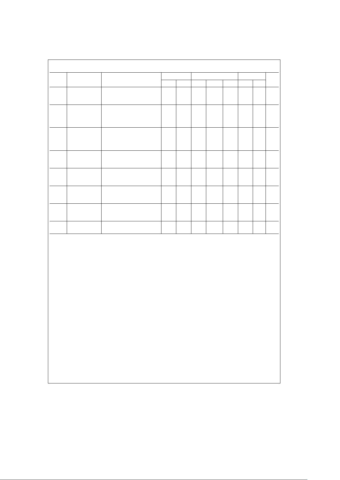
DC Electrical Characteristics CD4723BC/CD4724BC (Note 2)
Symbol Parameter Conditions
b
40§C
a
25§C
a
85§C
Units
Min Max Min Typ Max Min Max
I
DD
Quiescent Device V
DD
e
5V 20 0.02 20 150 mA
Current V
DD
e
10V 40 0.02 40 300 mA
V
DD
e
15V 80 0.02 80 600 mA
V
OL
Low Level
l
I
O
l
s
1 mA
Output Voltage V
DD
e
5V 0.05 0 0.05 0.05 V
V
DD
e
10V 0.05 0 0.05 0.05 V
V
DD
e
15V 0.05 0 0.05 0.05 V
V
OH
High Level
l
I
O
l
s
1 mA
Output Voltage V
DD
e
5V 4.95 4.95 5.0 4.95 V
V
DD
e
10V 9.95 9.95 10 9.95 V
V
DD
e
15V 14.95 14.95 15 14.95 V
V
IL
Low Level V
DD
e
5V, V
O
e
0.5V or 4.5V 1.5 2.25 1.5 1.5 V
Input Voltage V
DD
e
10V, V
O
e
1V or 9V 3.0 4.5 3.0 3.0 V
V
DD
e
15V, V
O
e
1.5V or 13.5V 4.0 6.75 4.0 4.0 V
V
IH
High Level V
DD
e
5V, V
O
e
0.5V or 4.5V 3.5 3.5 2.75 3.5 V
Input Voltage V
DD
e
10V, V
O
e
1V or 9V 7.0 7.0 5.5 7.0 V
V
DD
e
15V, V
O
e
1.5V or 13.5V 11.0 11.0 8.25 11.0 V
I
OL
Low Level Output V
DD
e
5V, V
O
e
0.4V 0.52 0.44 0.88 0.36 mA
Current V
DD
e
10V, V
O
e
0.5V 1.3 1.1 2.25 0.9 mA
(Note 3) V
DD
e
15V, V
O
e
1.5V 3.6 3.0 8.8 2.4 mA
I
OH
High Level Output V
DD
e
5V, V
O
e
4.6V
b
0.52
b
0.44b0.88
b
0.36 mA
Current V
DD
e
10V, V
O
e
9.5V
b
1.3
b
1.1b2.25
b
0.9 mA
(Note 3) V
DD
e
15V, V
O
e
13.5V
b
3.6
b
3.0b8.8
b
2.4 mA
I
IN
Input Current V
DD
e
15V, V
IN
e
0V
b
0.30
b
10
b
5
b
0.30
b
1.0 mA
V
DD
e
15V, V
IN
e
15V 0.30 10
b
5
0.30 1.0 mA
Note 1: ‘‘Absolute Maximum Ratings’’ are those values beyond which the safety of the device cannot be guaranteed; they are not meant to imply that the devices
should be operated at these limits. The tables of ‘‘Recommended Operating Conditions’’ and Electrical Characteristics’’ provide conditions for actual device
operation.
Note 2: V
SS
e
0V unless otherwise specified.
Note 3: I
OL
and IOHare tested one output at a time.
3
Page 4

AC Electrical Characteristics*
T
A
e
25§C, C
L
e
50 pF, R
L
e
200k, Input t
r
e
t
f
e
20 ns, unless otherwise noted
Symbol Parameter Conditions Min Typ Max Units
t
PHL, tPLH
Propagation Delay V
DD
e
5V 200 400 ns
Data to Output V
DD
e
10V 75 150 ns
V
DD
e
15V 50 100 ns
t
PLH,tPHL
Propagation Delay V
DD
e
5V 200 400 ns
Enable to Output V
DD
e
10V 80 160 ns
V
DD
e
15V 60 120 ns
t
PHL
Propagation Delay V
DD
e
5V 175 350 ns
Clear to Output V
DD
e
10V 80 160 ns
V
DD
e
15V 65 130 ns
t
PLH,tPHL
Propagation Delay V
DD
e
5V 225 450 ns
Address to Output V
DD
e
10V 100 200 ns
V
DD
e
15V 75 150 ns
t
THL,tTLH
Transition Time V
DD
e
5V 100 200 ns
(Any Output) V
DD
e
10V 50 100 ns
V
DD
e
15V 40 80 ns
TWH,T
WL
Minimum Data V
DD
e
5V 100 200 ns
Pulse Width V
DD
e
10V 50 100 ns
V
DD
e
15V 40 80 ns
tWH,t
WL
Minimum Address V
DD
e
5V 200 400 ns
Pulse Width V
DD
e
10V 100 200 ns
V
DD
e
15V 65 125 ns
t
WH
Minimum Clear V
DD
e
5V 75 150 ns
Pulse Width V
DD
e
10V 40 75 ns
V
DD
e
15V 25 50 ns
t
SU
Minimum Setup Time V
DD
e
5V 40 80 ns
Data to E V
DD
e
10V 20 40 ns
V
DD
e
15V 15 30 ns
t
H
Minimum Hold Time V
DD
e
5V 60 120 ns
Data to E V
DD
e
10V 30 60 ns
V
DD
e
15V 25 50 ns
t
SU
Minimum Setup Time V
DD
e
5V
b
15 50 ns
Address to E V
DD
e
10V 0 30 ns
V
DD
e
15V 0 20 ns
t
H
Minimum Hold Time V
DD
e
5V
b
50 15 ns
Address to E V
DD
e
10V
b
20 10 ns
V
DD
e
15V
b
15 5 ns
C
PD
Power Dissipation Per Package
100 pF
Capacitance (Note 4)
C
IN
Input Capacitance Any Input 5.0 7.5 pF
*AC Parameters are guaranteed by DC correlated testing.
Note 1: ‘‘Absolute Maximum Ratings’’ are those values beyond which the safety of the device cannot be guaranteed; they are not meant to imply that the devices
should be operated at these limits. The tables of ‘‘Recommended Operating Conditions’’ and Electrical Characteristics’’ provide conditions for actual device
operation.
Note 2: V
SS
e
0V unless otherwise specified.
Note 3: I
OL
and IOHare tested one output at a time.
Note 4: Dynamic power dissipation (P
D
) is given by: P
D
e
(C
PD
a
CL)V
CC
2
faPQ; where C
L
e
load capacitance; fefrequency of operation; for further details,
see Application Note AN-90, ‘‘54C/74C Family Characteristics’’.
4
Page 5

Logic Diagrams
CD4723B
TL/F/6003– 3
5
Page 6

Logic Diagrams (Continued)
CD4724B
TL/F/6003– 4
6
Page 7

Switching Time Waveforms
TL/F/6003– 5
7
Page 8

CD4723BM/CD4723BC Dual 4-Bit Addressable Latch
CD4724BM/CD4724BC 8-Bit Addressable Latch
Physical Dimensions inches (millimeters)
Ceramic Dual-In-Line Package (J)
Order Number CD4723BMJ, CD4723BCJ, CD4724BMJ or CD4724BCJ
NS Package Number J16A
Molded Dual-In-Line Package (N)
Order Number CD4723BMN, CD4723BCN, CD4724BMN or CD4724BCN
NS Package Number N16E
LIFE SUPPORT POLICY
NATIONAL’S PRODUCTS ARE NOT AUTHORIZED FOR USE AS CRITICAL COMPONENTS IN LIFE SUPPORT
DEVICES OR SYSTEMS WITHOUT THE EXPRESS WRITTEN APPROVAL OF THE PRESIDENT OF NATIONAL
SEMICONDUCTOR CORPORATION. As used herein:
1. Life support devices or systems are devices or 2. A critical component is any component of a life
systems which, (a) are intended for surgical implant support device or system whose failure to perform can
into the body, or (b) support or sustain life, and whose be reasonably expected to cause the failure of the life
failure to perform, when properly used in accordance support device or system, or to affect its safety or
with instructions for use provided in the labeling, can effectiveness.
be reasonably expected to result in a significant injury
to the user.
National Semiconductor National Semiconductor National Semiconductor National Semiconductor
Corporation Europe Hong Kong Ltd. Japan Ltd.
1111 West Bardin Road Fax: (
a
49) 0-180-530 85 86 13th Floor, Straight Block, Tel: 81-043-299-2309
Arlington, TX 76017 Email: cnjwge@tevm2.nsc.com Ocean Centre, 5 Canton Rd. Fax: 81-043-299-2408
Tel: 1(800) 272-9959 Deutsch Tel: (
a
49) 0-180-530 85 85 Tsimshatsui, Kowloon
Fax: 1(800) 737-7018 English Tel: (
a
49) 0-180-532 78 32 Hong Kong
Fran3ais Tel: (
a
49) 0-180-532 93 58 Tel: (852) 2737-1600
Italiano Tel: (
a
49) 0-180-534 16 80 Fax: (852) 2736-9960
National does not assume any responsibility for use of any circuitry described, no circuit patent licenses are implied and National reserves the right at any time without notice to change said circuitry and specifications.
 Loading...