

Page 1
October 1987
Revised January 1999
CD4724BC 8-Bit Addressable Latch
© 1999 Fairchild Semiconductor Corporation DS006003.prf www.fairchildsemi.com
CD4724BC
8-Bit Addressable Latch
General Description
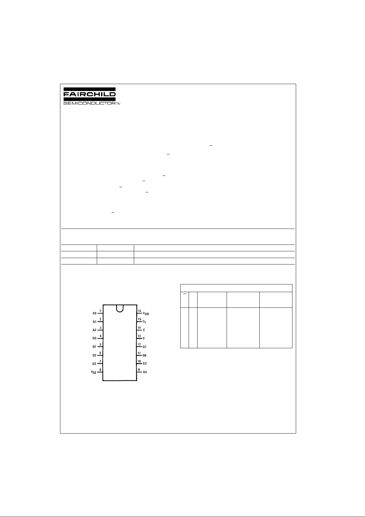
The CD4724BC is an 8 -bit addressable latch with three
address inputs (A0–A2), an active low enable input (E
),
active high clear input (CL), a d ata inpu t (D) and eigh t outputs (Q0–Q7).
Data is entered into a particular bit in the latch when that is
addressed by the address inputs and the enable (E
) is
LOW. Data entry is inhibited when enable (E
) is HIGH.
When clear (CL) and e nable (E
) are HIGH, all outputs are
LOW. When clear (CL) is HIGH and enable (E
) is LOW, the
channel demultiplexing occurs. Th e bit that is addressed
has an active output which follows the data input while all
unaddressed bits are held LOW. When operating in the
addressable latch mode (E
= CL = LOW), changing more
than one bit of the address cou ld impo se a tra nsi en t wro ng
address. Therefore, this should only be done while in the
memory mode (E
= HIGH, CL = LOW).
Features
■ Wide supply voltage range: 3.0V to 15V
■ High noise immunity: 0.45 V
DD
(typ.)
■ Low power TTL compatibility:
fan out of 2 driving 74L or 1 driving 74LS
■ Serial to parallel capability
■ Storage register capability
■ Random (addressable) data entry
■ Active high demultiplexing capability
■ Common active high clear
Ordering Code:
Devices also available in Tape and Reel. Specify by appending the suffix letter “X” to t he ordering code.
Connection Diagram
Pin Assignments for DIP and SOIC
Top View
Truth Table
Order Number Package Number Package Description
CD4724BCM M16A 16-Lead Small Outline Integrated Circuit (SOIC), JEDEC MS-012, 0.150” Narrow Body
CD4724BCN N16E 16-Lead Plastic Dual-In-Line Package (PDIP), JEDEC MS-001, 0.300” Wide
Mode Selection
E
CL Addressed Unaddressed Mode
Latch Latch
L L Follows Data Holds Previous
Data
Addressable
Latch
H L Hold Previous
Data
Holds Previous
Data
Memory
L H Follows Data Reset to “0” Demultiplexer
H H Reset to “0” Reset to “0” Clear
Page 2
www.fairchildsemi.com 2
CD4724BC
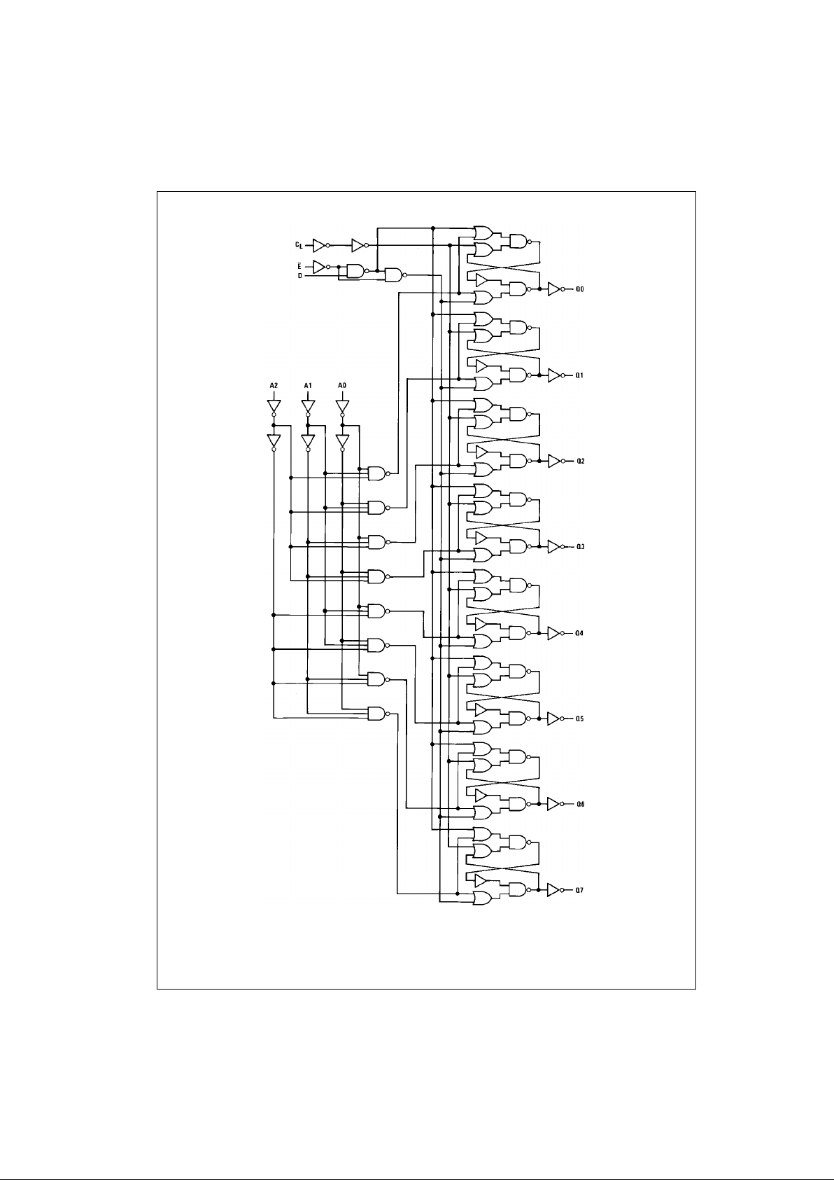
Logic Diagram
Page 3
3 www.fairchildsemi.com
CD4724BC
Absolute Maximum Ratings(Note 1)
(Note 2)
Recommended Operating
Conditions
(Note 2)
Note 1: “Absolute Maximum Rat ings” are tho se values beyond which the
safety of the device cannot be guaranteed; they are not meant to imply that
the devices should be o perated at these limits. The tables of “R ecommended Operating Cond itions ” and Electr ical Cha racteris tics” provide c onditions for actual device operat ion.
Note 2: V
SS
= 0V unless otherw is e s pecified.
DC Electrical Characteristics (Note 2)
Note 3: IOL and IOH are tested one output at a ti m e.
DC Supply Voltage (VDD) −0.5V to +18 V
DC
Input Voltage (VIN) −0.5V to VDD +0.5 V
DC
Storage Temperature (TS) −65°C to +150°C
Power Dissipation (P
D
)
Dual-In-Line 700 mW
Small Outline 500 mW
Lead Temperature (T
L
)
(Soldering, 10 seconds ) 260°C
DC Supply Voltage (V
DD
) 3.0V to 15 V
DC
Input Voltage (VIN) 0V to VDD V
DC
Operating Temperature Range (TA) −40°C to +85°C
Symbol Parameter Conditions
−40°C +25°C +85°C
Units
Min Max Min Typ Max Min Max
I
DD
Quiescent Device VDD = 5V 20 0.02 20 150 µA
Current VDD = 10V 40 0.02 40 300 µA
VDD = 15V 80 0.02 80 600 µA
V
OL
LOW Level |IO| ≤ 1 µA
Output Voltage VDD = 5V 0.05 0 0.05 0.05 V
VDD = 10V 0.05 0 0.05 0.05 V
VDD = 15V 0.05 0 0.05 0.05 V
V
OH
HIGH Level |IO| ≤ 1 µA
Output Voltage VDD = 5V 4.95 4.95 5.0 4.95 V
VDD = 10V 9.95 9.95 10 9.95 V
VDD = 15V 14.95 14.95 15 14.95 V
V
IL
LOW Level VDD = 5V, VO = 0.5V or 4.5V 1.5 2.25 1.5 1.5 V
Input Voltage VDD = 10V, VO = 1V or 9V 3.0 4.5 3.0 3.0 V
VDD = 15V, VO = 1.5V or 13.5V 4.0 6.75 4.0 4.0 V
V
IH
HIGH Level VDD = 5V, VO = 0.5V or 4.5V 3.5 3.5 2.75 3.5 V
Input Voltage VDD = 10V, VO = 1V or 9V 7.0 7.0 5.5 7.0 V
VDD = 15V, VO = 1.5V or 13.5V 11.0 11.0 8.25 11.0 V
I
OL
LOW Level Output VDD = 5V, VO = 0.4V 0.52 0.44 0.88 0.36 mA
Current VDD = 10V, VO = 0.5V 1.3 1.1 2.25 0.9 mA
(Note 3) VDD = 15V, VO = 1.5V 3.6 3.0 8.8 2.4 mA
I
OH
HIGH Level Output VDD = 5V, VO = 4.6V −0.52 −0.44 −0.88 −0.36 mA
Current VDD = 10V, VO = 9.5V −1.3 −1.1 −2.25 −0.9 mA
(Note 3) VDD = 15V, VO = 13.5V −3.6 −3.0 −8.8 −2.4 mA
I
IN
Input Current VDD = 15V, VIN = 0V −0.30 −10−5−0.30 −1.0 µA
VDD = 15V, VIN = 15V 0.30 10−50.30 1.0 µA
Page 4

www.fairchildsemi.com 4
CD4724BC
AC Electrical Charac teristics (Note 4)
TA = 25°C, CL = 50 pF, RL = 200k, Input tr = tf = 20 ns, unless otherwise noted
Note 4: AC Parameters are guara nt eed by DC correlated testing.
Note 5: Dynamic power dissipat ion (P
D
) is given by: PD = (CPD + CL) V
CC
2
f + PQ; where CL = load capacitance; f = frequency o f operation; for further det ails,
see Application N ot e AN-90, “Family Characteris t ic s ”.
Symbol Parameter Conditions Min Typ Max Units
t
PHL, tPLH
Propagation Delay VDD = 5V 200 400 ns
Data to Output VDD = 10V 75 150 ns
VDD = 15V 50 100 ns
t
PLH
, t
PHL
Propagation Delay VDD = 5V 200 400 ns
Enable to Output VDD = 10V 80 160 ns
VDD = 15V 60 120 ns
t
PHL
Propagation Delay VDD = 5V 175 350 ns
Clear to Output VDD = 10V 80 160 ns
VDD = 15V 65 130 ns
t
PLH
, t
PHL
Propagation Delay VDD = 5V 225 450 ns
Address to Output VDD = 10V 100 200 ns
VDD = 15V 75 150 ns
t
THL
, t
TLH
Transition Time VDD = 5V 100 200 ns
(Any Output) VDD = 10V 50 100 ns
VDD = 15V 40 80 ns
TWH, T
WL
Minimum Data VDD = 5V 100 200 ns
Pulse Width VDD = 10V 50 100 ns
VDD = 15V 40 80 ns
tWH, t
WL
Minimum Address VDD = 5V 200 400 ns
Pulse Width VDD = 10V 100 200 ns
VDD = 15V 65 125 ns
t
WH
Minimum Clear VDD = 5V 75 150 ns
Pulse Width VDD = 10V 40 75 ns
VDD = 15V 25 50 ns
t
SU
Minimum Setup Time VDD = 5V 40 80 ns
Data to E VDD = 10V 20 40 ns
VDD = 15V 15 30 ns
t
H
Minimum Hol d Time VDD = 5V 60 120 ns
Data to E VDD = 10V 30 60 ns
VDD = 15V 25 50 ns
t
SU
Minimum Setup Time VDD = 5V −15 50 ns
Address to E VDD = 10V 0 30 ns
VDD = 15V 0 20 ns
t
H
Minimum Hol d Time VDD = 5V −50 15 ns
Address to E VDD = 10V −20 10 ns
VDD = 15V −15 5 ns
C
PD
Power Dissipation Per Packa ge 100 pF
Capacitance (Note 5)
C
IN
Input Capacitance Any Input 5.0 7.5 pF
Page 5

5 www.fairchildsemi.com
CD4724BC
Switching Time Waveforms
Page 6

www.fairchildsemi.com 6
CD4724BC
Physical Dimensions inches (millimeters) unless otherwise noted
16-Lead Small Outline Integrated Circuit (SOIC), JEDEC MS-012, 0.150” Narrow Body
Package Number M16A
Page 7

Fairchild does not assume any responsibility for use of any circuitry described, no circui t patent licenses are implied and Fairchild reserves the right at any time without notice to change said circuitry and specifications.
CD4724BC 8-Bit Addressable Latch
LIFE SUPPORT POLICY
FAIRCHILD’S PRODUCTS ARE NOT AUTHORIZED FOR USE AS CRITICAL COMPONENTS IN LIFE SUPPORT
DEVICES OR SYSTEMS WITHOUT THE EXPRESS WRITTEN APPROVAL OF THE PRESIDENT OF FAIRCHILD
SEMICONDUCTOR CORPORATION. As used herein:
1. Life support devices or system s a re devices or syste ms
which, (a) are intended for surgical implant into the
body, or (b) support or sustain life, and (c) whose failure
to perform when properly used in accordance with
instructions for use provided in the labeling, can be reasonably expected to result in a significant injur y to the
user.
2. A critical compon ent in any com ponent of a li fe support
device or system whose failure to p erform can be r easonably expected to cause the failure of the life suppor t
device or system, or to affect its safety or effectiveness.
www.fairchildsemi.com
Physical Dimensions inches (millimeters) unless otherwise noted (Continued)
16-Lead Plastic Dual-In-Line Package (PDIP), JEDEC MS-001, 0.300” Wide
Package Number N16E
 Loading...