

Page 1
October 1987
Revised March 1999
CD4541BC Programmable Timer
© 1999 Fairchild Semiconductor Corporation DS006001.prf www.fairchildsemi.com
CD4541BC
Programmable Timer
General Description
The CD4541BC Program mable Timer is designed with a
16-stage binary counter, an integrated oscillator for use
with an external capac itor and two resi stors, output control
logic, and a special power-on reset circuit. The special features of the power-on rese t circuit are first, no additional
static power consumpt ion and second, the part functio ns
across the full voltage range (3V–15V ) whether power-on
reset is enabled or disabled.
Timing and the counter are in itialized by tur ning on po wer,
if the power-on reset is enabled. When the power is
already on, an external reset pulse will also initialize the
timing and counter. After either r eset is accomplished , the
oscillator frequency is determined by t he external RC network. The 16-stage counter divides the oscillator frequency
by any of 4 digitally controlled division ratios.
Features
■ Available division ratios 28, 210, 213, or 2
16
■ Increments on positive edge clock transitions
■ Built-in low power RC oscillator (±2% accuracy over
temperature rang e and ±10 % suppl y and ±3% over processing @ < 10 kHz)
■ Oscillator frequency range ≈ DC to 100 kHz
■ Oscillator may be bypassed if external clock is available
(apply external cloc k to pin 3)
■ Automatic reset initializes all counters when power turns
on
■ External master reset t otally independent of automatic
reset operation
■ Operates at 2
n
frequency divider or single transition
timer
■ Q/Q
select provides output logic level flexibility
■ Reset (auto or ma ster) disables oscillator du ring resetting to provide no active power dissipation
■ Clock conditioning circuit permits operation with very
slow clock rise and fall times
■ Wide supply voltage range—3.0V to 15V
■ High noise immunity—0.45 V
DD
(typ.)
■ 5V–10V–15V parameter ratings
■ Symmetrical output characteristics
■ Maximum input leaka ge 1 µA at 15V over full tempera-
ture range
■ High output drive (pin 8) min. one TTL load
Ordering Code:
Devices also availab le in Tape and Reel. Specify by appending th e s uffix let t er “X” to the ordering code.
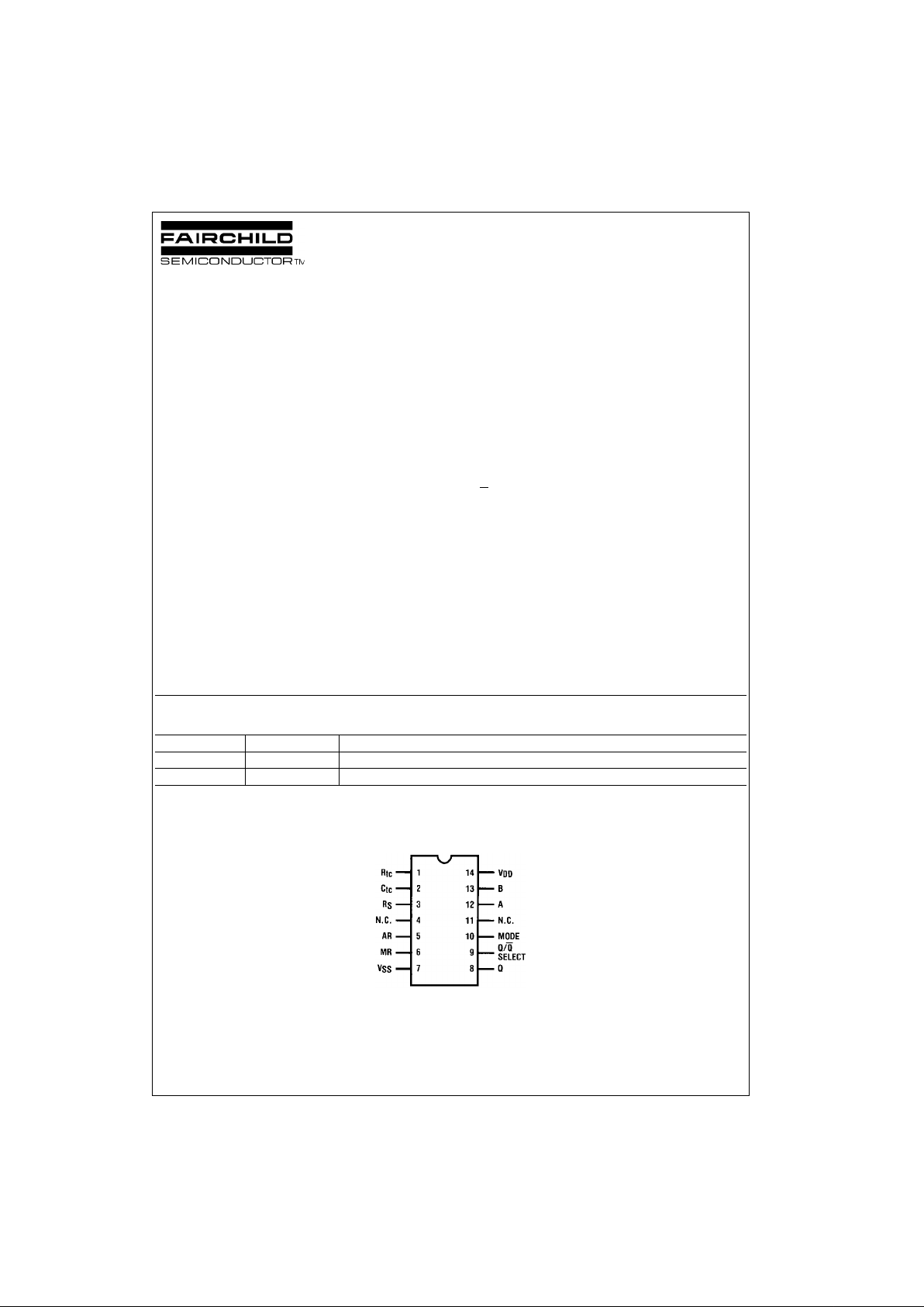
Connection Diagram
Pin Assignments for DIP and SOIC
N.C.—Not connected
Top View
Order Number Package Number Package Description
CD4541BCN N14A 14-Lead Plastic Dual-In-Line Package (PDIP), JEDEC MS-001, 0.300” Wide
CD4541BCM M14A 14-Lead Small Outline Integrated Circuit (SOIC), JEDEC MS-012, 0.150” Narrow
Page 2
www.fairchildsemi.com 2
CD4541BC
Truth Table Division Ratio Table
Operating Characteristics
With Auto Reset pin set to a “0” the counte r circu it is initialized by turning on power. Or with power already on , the
counter circuit is reset when the Ma ster Re set pin is set to
a “1”. Both types of reset will result in synchronously resetting all counter stages independent of counter state.
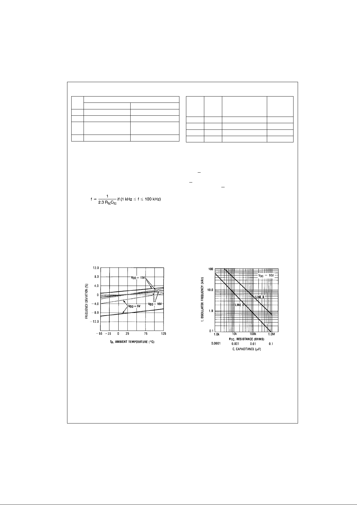
The RC oscillator frequency is determined by the external
RC network, i.e.:
and R
S
≈ 2 Rtc where RS ≥ 10 kΩ
The time select inputs (A and B) provide a two-bit address
to output any one of f our counter sta ges (2
8
, 210, 213, and
2
16
). The 2n counts as shown in the Division Ratio Table
represent the Q output of the Nth stage of the counter.
When A is “1”, 2
16
is selected for both states of B.
However, when B is “0”, normal counting is interrupted and
the 9th counter stage receives its clock directly from the
oscillator (i.e., effectively outputting 2
8
).
The Q/Q
select output control pin provides for a choice of
output level. When the counter is in a r eset condition and
Q/Q
select pin is set to a “0” the Q ou tput is a “0”. Corre-
spondingly, when Q/Q
select pin is set to a “1” the Q output
is a “1”.
When the mode control pin is set to a “1”, the selected
count is continually transmitted to the output. But, with
mode pin “0” and after a reset conditi on the RS flip-flop
resets (see Logic Diagram), counting commences and after
2
n−1
counts the RS flip-flop sets which causes the output to
change state. Hence, af ter another 2
n−1
counts the output
will not change. Thus, a Master Reset pulse must be
applied or a chang e in the mode pin lev el is required to
reset the single cycle operation.
Typical RC Oscillator
Characteristics
Solid Line = RTC = 56 kΩ, RS = 1 kΩ and C = 1000 pF
f = 10.2 kHz @ V
DD
= 10V and TA = 25°
Dashed Line = R
TC
= 56 kΩ, RS = 120 kΩ and C = 1000 pF
f = 7.75 kHz @ V
DD
= 10V and TA = 25°
RC Oscillator Frequency as a
Function of R
TC
and C
Line A: f as a function of C and (RTC = 56 kΩ; RS = 120k
Line B: f as a function of R
TC
and (C = 100 pF; RS = 2 R
TC
Pin State
01
5 Auto Reset Operating Auto Reset Disabled
6 Timer Operational Master Reset On
9 Output Initially Low Output Initially High
after Reset after Reset
10 Single Cycle Mode Re cycle Mod e
Number of Count
A B Counter Stages
2
n
n
0 0 13 8192
0 1 10 1024
10 8 256
1 1 16 65536
Page 3
3 www.fairchildsemi.com
CD4541BC
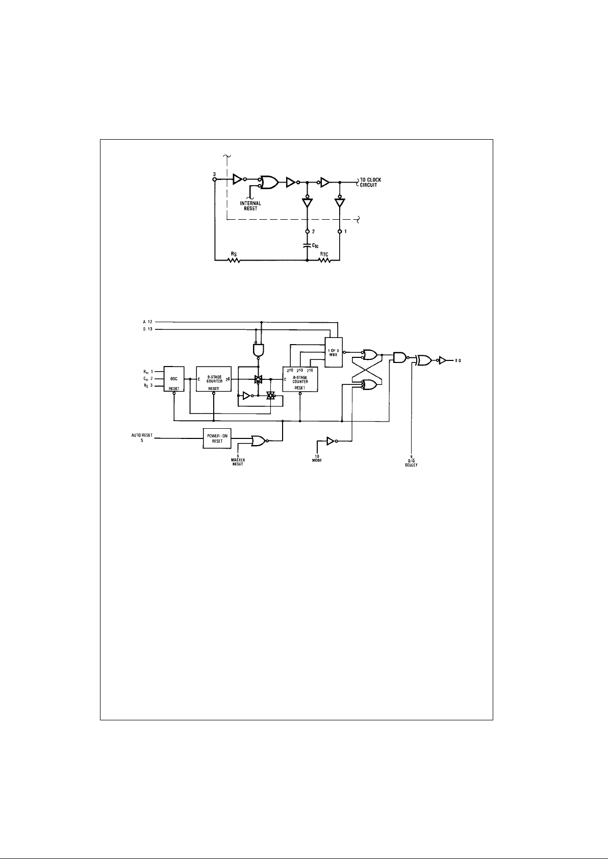
Oscillator Circuit Using RC Configuration
Logic Diagram
VDD = Pin 14
V
SS
= Pin 7
Page 4

www.fairchildsemi.com 4
CD4541BC
Absolute Maximum Ratings(Note 1)
(Note 2)
Recommended Operating
Conditions
(Note 2)
Note 1: “Absolute Maximum Ratings” ar e those value s beyond which the
safety of the device cannot be guaranteed. Except for “Operating Temperature Range” they are not m eant to i mply that t he devices should be operated at these limits. The table of “Electrical Characteristics” provides
conditions for actua l device operation.
Note 2: V
SS
= 0V unless otherw is e s pecified.
DC Electrical Characteristics (Note 2)
Note 3: IOH and IOL are tested one output at a time.
Supply Voltage (VDD) −0.5V to +18V
Input Voltage (V
IN
) −0.5V to VDD +0.5V
Storage Temperature Range (T
S
) −65°C to +150°C
Power Dissipation (P
D
)
Dual-In-Line 700 mW
Small Outline 500 mW
Lead Temperature (T
L
)
(soldering, 10 seconds) 260°C
Supply Voltage (V
DD
) 3V to 15V
Input Voltage (V
IN
) 0 to V
DD
Operating Temperatur e Range −40°C to +85°C
Symbol Parameter Conditions
−40°C +25°C +85°C
Units
Min Max Min Typ Max Min Max
I
DD
Quiescent Device Current VDD = 5V, VIN = VDD or V
SS
20 0.005 20 150 µA
VDD = 10V, VIN = VDD or V
SS
40 0.010 40 300 µA
VDD = 15V, VIN = VDD or V
SS
80 0.015 80 600 µA
V
OL
LOW Level Output Voltage VDD = 5V 0.05 0 0.05 0.05 V
VDD = 10V |IO| < 1µA 0.05 0 0.05 0.05 V
VDD = 15V 0.05 0 0.05 0.05 V
V
OH
HIGH Level Output Voltage VDD = 5V 4.95 4.95 5 4.95 V
VDD = 10V |IO| < 1 µA 9.95 9.95 10 9.95 V
VDD = 15V 14.95 14.95 15 14.95 V
V
IL
LOW Level Input Voltage VDD = 5V, VO = 0.5V or 4.5V 1.5 2 1.5 1.5 V
VDD = 10V, VO = 1.0V or 9.0V 3.0 4 3.0 3.0 V
VDD = 15V, VO = 1.5V or 13.5V 4.0 6 4.0 4.0 V
V
IH
HIGH Level Input Voltage VDD = 5V, VO = 0.5V or 4.5V 3.5 3.5 3 3.5 V
VDD = 10V, VO = 1.0V or 9.0V 7.0 7.0 6 7.0 V
VDD = 15V, VO = 1.5V or 13.5V 11.0 11.0 9 11.0 V
I
OL
LOW Level Output Current VDD = 5V, VO = 0.4V 2.32 1.96 3.6 1.6 mA
(Note 3) VDD = 10V, VO = 0.5V 3.18 2.66 9.0 2.18 mA
VDD = 15V, VO = 1.5V 12.4 10.4 34.0 8.50 mA
I
OH
HIGH Level Output Current VDD = 5V, VO = 2.5V 5.1 4.27 130 3.5 mA
(Note 3) VDD = 10V, VO = 9.5V 2.69 2.25 8.0 1.85 mA
VDD = 15V, VO = 13.5V 10.5 8.8 30.0 7.22 mA
I
IN
Input Current VDD = 15V, VIN = 0V −0.3 −10−5−0.3 −1.0 µA
VDD = 15V, VIN = 15V 0.3 10−50.3 1.0 µA
Page 5

5 www.fairchildsemi.com
CD4541BC
AC Electrical Characteristics (Note 4)
TA = 25°C, CL = 50 pF (refer to test circuits)
Note 4: AC Parameters are guaranteed by DC c orrelated testing.
Note 5: C
PD
determines the no load AC powe r consumption of any CMOS device . For complete ex planation , see Family Charac teristics application note:
AN-90.
Symbol Parameter Conditions Min Typ Max Units
t
TLH
Output Rise Time VDD = 5V 50 200 ns
VDD = 10V 30 100 ns
VDD = 15V 25 80 ns
t
THL
Output Fall Time VDD = 5V 50 200 ns
VDD = 10V 30 100 ns
VDD = 15V 25 80 ns
t
PLH, tPHL
Turn-Off, Turn-On Propagation Delay, VDD = 5V 1.8 4.0 µs
Clock to Q (28 Output) VDD = 10V 0.6 1.5 µs
VDD = 15V 0.4 1.0 µs
t
PHL, tPLH
Turn-On, Turn-Off Propagation Delay, VDD = 5V 3.2 8.0 µs
Clock to Q (216 Output) VDD = 10V 1.5 3.0 µs
VDD = 15V 1.0 2.0 µs
t
WH(CL)
Clock Pulse Width VDD = 5V 400 200 ns
VDD = 10V 200 100 ns
VDD = 15V 150 70 ns
f
CL
Clock Pulse Frequency VDD = 5V 2.5 1.0 MHz
VDD = 10V 6.0 3.0 MHz
VDD = 15V 8.5 4.0 MHz
t
WH(R)
MR Pulse Width VDD = 5V 400 170 ns
VDD = 10V 200 75 ns
VDD = 15V 150 50 ns
C
I
Average Input Capacitance Any Input 5.0 7.5 pF
C
PD
Power Dissipation Capacitance (Note 5) 100 pF
Page 6
www.fairchildsemi.com 6
CD4541BC
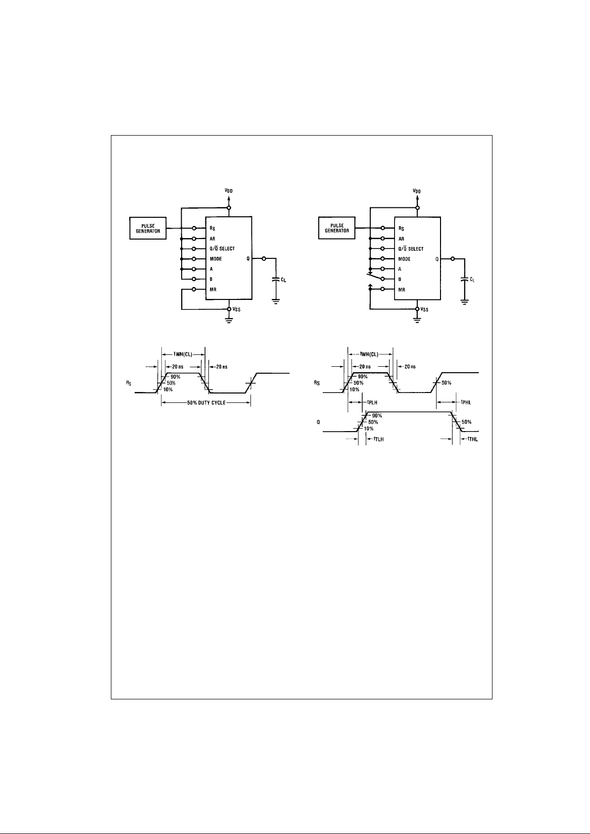
Test Circuits and Waveforms
Power Dissipation Test
Circuit and Waveforms
(Rtc and Ctc outputs are left open)
Switching Time Test
Circuit and Waveforms
C
Page 7

7 www.fairchildsemi.com
CD4541BC
Physical Dimensions inches (millimeters) unless otherwise noted
14-Lead Plastic Dual-In-Line Package (PDIP), JEDEC MS-001, 0.300” Wide
Package Number N14A
Page 8

Fairchild does not assume any responsibility for use of any circuitry described, no circuit patent licenses are implied and Fairchild reserves the right at any time without notice to change said circuitry and specifications.
CD4541BC Programmable Timer
LIFE SUPPORT POLICY
FAIRCHILD’S PRODUCTS ARE NOT AUTHORIZED FOR USE AS CRITICAL COMPONENTS IN LIFE SUPPORT
DEVICES OR SYSTEMS WITHOUT THE EXPRESS WRITTEN APPROVAL OF THE PRESIDENT OF FAIRCHILD
SEMICONDUCTOR CORPORATION. As used herein:
1. Life support devices or systems are devices or syste ms
which, (a) are intended for surgical implant into the
body, or (b) support or sustain life, and (c) whose failure
to perform when properly used in accordance with
instructions for use provided in the labeling, can be reasonably expected to result in a significant inju ry to the
user.
2. A critical component i n any compon ent of a lif e support
device or system whose failu re to perform can be reasonably expected to ca use the fa i lure of the life su pp ort
device or system, or to affect its safety or effectiveness.
www.fairchildsemi.com
Physical Dimensions inches (millimeters) unless otherwise noted (Continued)
14-Lead Small Outline Integrated Circuit (SOIC), JEDEC MS-012, 0.150” Narrow
Package Number M16A
 Loading...