

Page 1
CD4536BMS
December 1992
Features
• High Voltage Type (20V Rating)
0
24
• 24 Flip-Flop Stage - Counts from 2
• Last 16 Stages Selectable by BCD Select Code
• Bypass Input Allows Bypassing First 8 Stages
• On-Chip RC Oscillator Provision
• Clock Inhibit Input
• Schmitt Trigger in clock Line Permits Operation with
Very Long Rise and Fall Times
• On-Chip Monostable Output Provision
• Typical fCL = 3MHz at VDD = 10V
• Test Mode Allows Fast Test Sequence
• Set and Reset Inputs
• Capable of Driving Two Low Power TTL Loads, One
Lower Power Schottky Load, or Two HTL Loads Over
the Rated Temperature Range
• 100% Tested for Quiescent Current at 20V
• 5V, 10V and 15V Parametric Ratings
• Standardized, Symmetrical Output Characteristics
• Meets All Requirements of JEDEC Tentative Standard
No. 13B, “Standard Specifications for Description of
‘B’ Series CMOS Devices”
to 2
CMOS Programmable Timer
Description
CD4536BMS is a programmable timer consisting of 24 ripple
binary counter stages. The salient feature of this device is its
flexibility. The device can count from 1 to 2
stages can be bypassed to allow an output, selectable by a
4-bit code, from any one of the remaining 16 stages. It can
be driven by an external clock or an RC oscillator that can be
constructed using on-chip components. Input IN1 serves as
either the external clock input or the input to the on-chip RC
oscillator. OUT1 and OUT2 are connection terminals for the
external RC components. In addition, an on-chip monostable
circuit is provided to allow a variable pulse width output. V arious timing functions can be achieved using combinations of
these capabilities.
A logic 1 on the 8-BYPASS input enables a bypass of the
first 8 stages and makes stage 9 the first counter stage of
the last 16 stages. Selection of 1 of 16 outputs is accomplished by the decoder and the BCD inputs A, B, C and D.
MONO IN is the timing input for the on-chip monostable
oscillator. Grounding of the MONO IN terminal through a
resistor of 10kΩ or higher, disables the one-shot circuit and
connects the decoder directly to the DECODE OUT terminal.
A resistor to VDD and a capacitor to ground from the MONO
IN terminal enables the one-shot circuit and controls its
pulse width.
A fast test mode is enabled by a logic 1 on 8-BYPASS, SET,
and RESET. This mode divides the 24-stage counter into
three 8-stage sections to facilitate a fast test sequence.
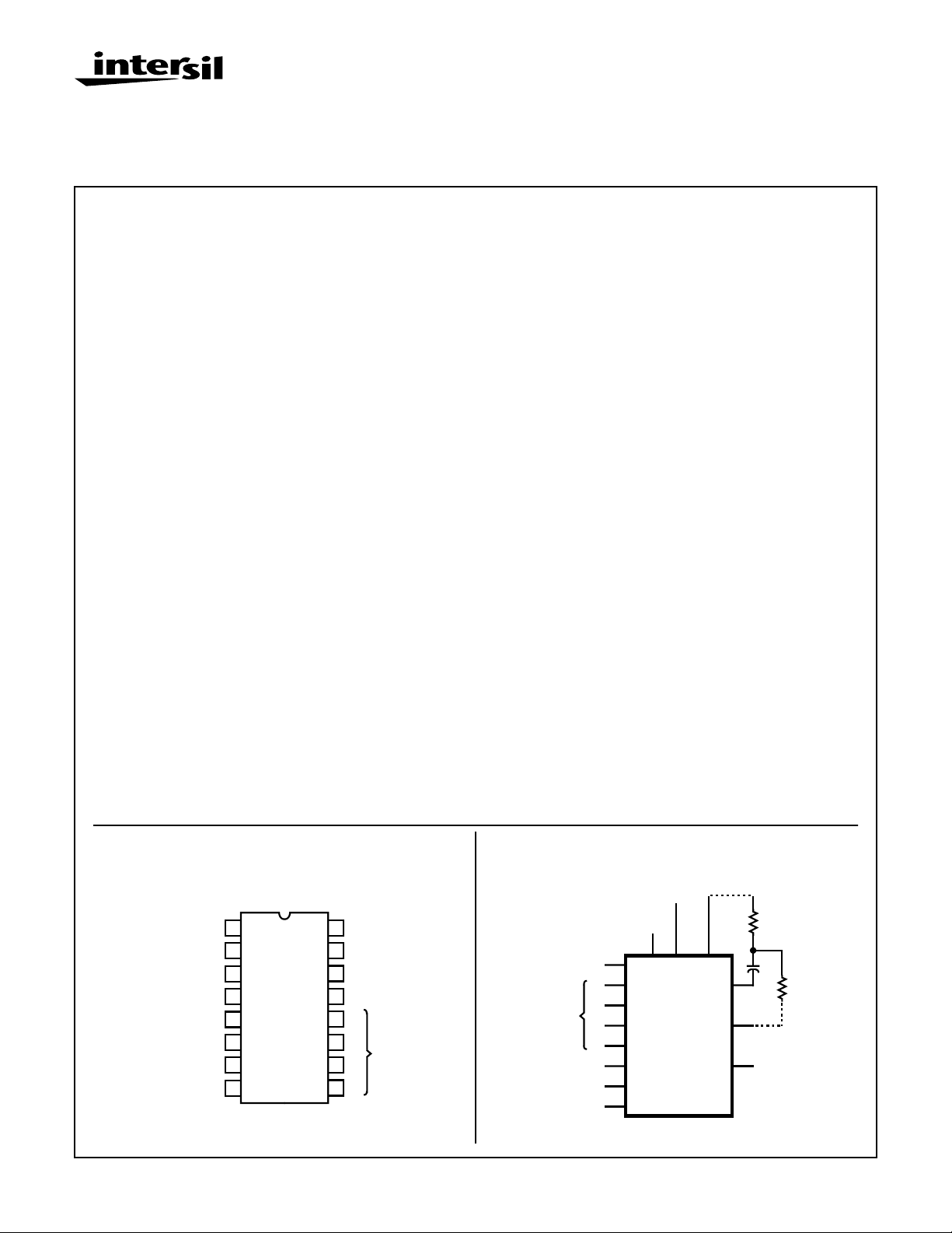
The CD4536BMS is supplied in these 16-lead outline packages:
24
or the first 8
Braze Seal DIP H4X
Frit Seal DIP H1F
Ceramic Flatpack H6W
Pinout
CD4536BMS
TOP VIEW
16
1
SET
IN 1
OUT 1
OUT 2
VSS
2
3
4
5
6
7
8
RESET
8-BYPASS
CLOCK INHIBIT
CAUTION: These devices are sensitive to electrostatic discharge; follow proper IC Handling Procedures.
1-888-INTERSIL or 321-724-7143 | Copyright © Intersil Corporation 1999
VDD
15
MONO IN
14
OSC INHIBIT
13
DECODE OUT
12
D
11
C
10
B
9
A
BINARY
SELECT
Functional Diagram
BINARY
SELECT
RESET
MONO IN
7-1236
8-BYPASS
6
9
A
10
B
11
C
12
D
1
SET
2
15
CLOCK
INHIBIT
OSC
INHIBIT
14
IN 1
73
RS
4
OUT 1
5
OUT 2
13
RT
DECODE
OUT
VSS = 8
VDD = 16
File Number
3345
Page 2
Specifications CD4536BMS
Absolute Maximum Ratings Reliability Information
DC Supply Voltage Range, (VDD) . . . . . . . . . . . . . . . -0.5V to +20V
(Voltage Referenced to VSS Terminals)
Input Voltage Range, All Inputs . . . . . . . . . . . . .-0.5V to VDD +0.5V
DC Input Current, Any One Input . . . . . . . . . . . . . . . . . . . . . . . .±10mA
Operating Temperature Range. . . . . . . . . . . . . . . . -55oC to +125oC
Package Types D, F, K, H
Storage Temperature Range (TSTG). . . . . . . . . . . -65oC to +150oC
Lead Temperature (During Soldering) . . . . . . . . . . . . . . . . . +265oC
At Distance 1/16 ± 1/32 Inch (1.59mm ± 0.79mm) from case for
10s Maximum
TABLE 1. DC ELECTRICAL PERFORMANCE CHARACTERISTICS
PARAMETER SYMBOL CONDITIONS (NOTE 1)
Supply Current IDD VDD = 20V, VIN = VDD or GND 1 +25oC-10µA
VDD = 18V, VIN = VDD or GND 3 -55oC-10µA
Input Leakage Current IIL VIN = VDD or GND VDD = 20 1 +25oC -100 - nA
VDD = 18V 3 -55oC -100 - nA
Input Leakage Current IIH VIN = VDD or GND VDD = 20 1 +25oC - 100 nA
VDD = 18V 3 -55oC - 100 nA
Output Voltage VOL15 VDD = 15V, No Load 1, 2, 3 +25oC, +125oC, -55oC - 50 mV
Output Voltage VOH15 VDD = 15V, No Load (Note 3) 1, 2, 3 +25oC, +125oC, -55oC 14.95 - V
Output Current (Sink) IOL5 VDD = 5V, VOUT = 0.4V 1 +25oC 0.53 - mA
Output Current (Sink) IOL10 VDD = 10V, VOUT = 0.5V 1 +25oC 1.4 - mA
Output Current (Sink) IOL15 VDD = 15V, VOUT = 1.5V 1 +25oC 3.5 - mA
Output Current (Source) IOH5A VDD = 5V, VOUT = 4.6V 1 +25oC - -0.53 mA
Output Current (Source) IOH5B VDD = 5V, VOUT = 2.5V 1 +25oC - -1.8 mA
Output Current (Source) IOH10 VDD = 10V, VOUT = 9.5V 1 +25oC - -1.4 mA
Output Current (Source) IOH15 VDD = 15V, VOUT = 13.5V 1 +25oC - -3.5 mA
N Threshold Voltage VNTH VDD = 10V, ISS = -10µA 1 +25oC -2.8 -0.7 V
P Threshold Voltage VPTH VSS = 0V, IDD = 10µA 1 +25oC 0.7 2.8 V
Functional F VDD = 2.8V, VIN = VDD or GND 7 +25oC VOH >
VDD = 20V, VIN = VDD or GND 7 +25oC
VDD = 18V, VIN = VDD or GND 8A +125oC
VDD = 3V, VIN = VDD or GND 8B -55oC
Input Voltage Low
(Note 2)
Input Voltage High
(Note 2)
Input Voltage Low
(Note 2)
Input Voltage High
(Note 2)
NOTES: 1. All voltages referenced to device GND, 100% testing being
implemented.
2. Go/No Go test with limits applied to inputs.
VIL VDD = 5V, VOH > 4.5V, VOL < 0.5V 1, 2, 3 +25oC, +125oC, -55oC - 1.5 V
VIH VDD = 5V, VOH > 4.5V, VOL < 0.5V 1, 2, 3 +25oC, +125oC, -55oC 3.5 - V
VIL VDD = 15V, VOH > 13.5V,
VOL < 1.5V
VIH VDD = 15V, VOH > 13.5V,
VOL < 1.5V
Thermal Resistance . . . . . . . . . . . . . . . . θ
Ceramic DIP and FRIT Package. . . . . 80oC/W 20oC/W
Flatpack Package . . . . . . . . . . . . . . . . 70oC/W 20oC/W
Maximum Package Power Dissipation (PD) at +125oC
For TA = -55oC to +100oC (Package Type D, F, K) . . . . . . 500mW
For TA = +100oC to +125oC (Package Type D, F, K). . . . . .Derate
Linearity at 12mW/oC to 200mW
Device Dissipation per Output Transistor . . . . . . . . . . . . . . . 100mW
For TA = Full Package Temperature Range (All Package Types)
Junction Temperature . . . . . . . . . . . . . . . . . . . . . . . . . . . . . . +175oC
GROUP A
SUBGROUPS TEMPERATURE
2 +125oC - 1000 µA
2 +125oC -1000 - nA
2 +125oC - 1000 nA
1, 2, 3 +25oC, +125oC, -55oC- 4 V
1, 2, 3 +25oC, +125oC, -55oC11 - V
3. For accuracy, voltage is measured differentially to VDD. Limit
is 0.050V max.
ja
LIMITS
VDD/2
VOL <
VDD/2
θ
jc
UNITSMIN MAX
V
7-1237
Page 3
Specifications CD4536BMS
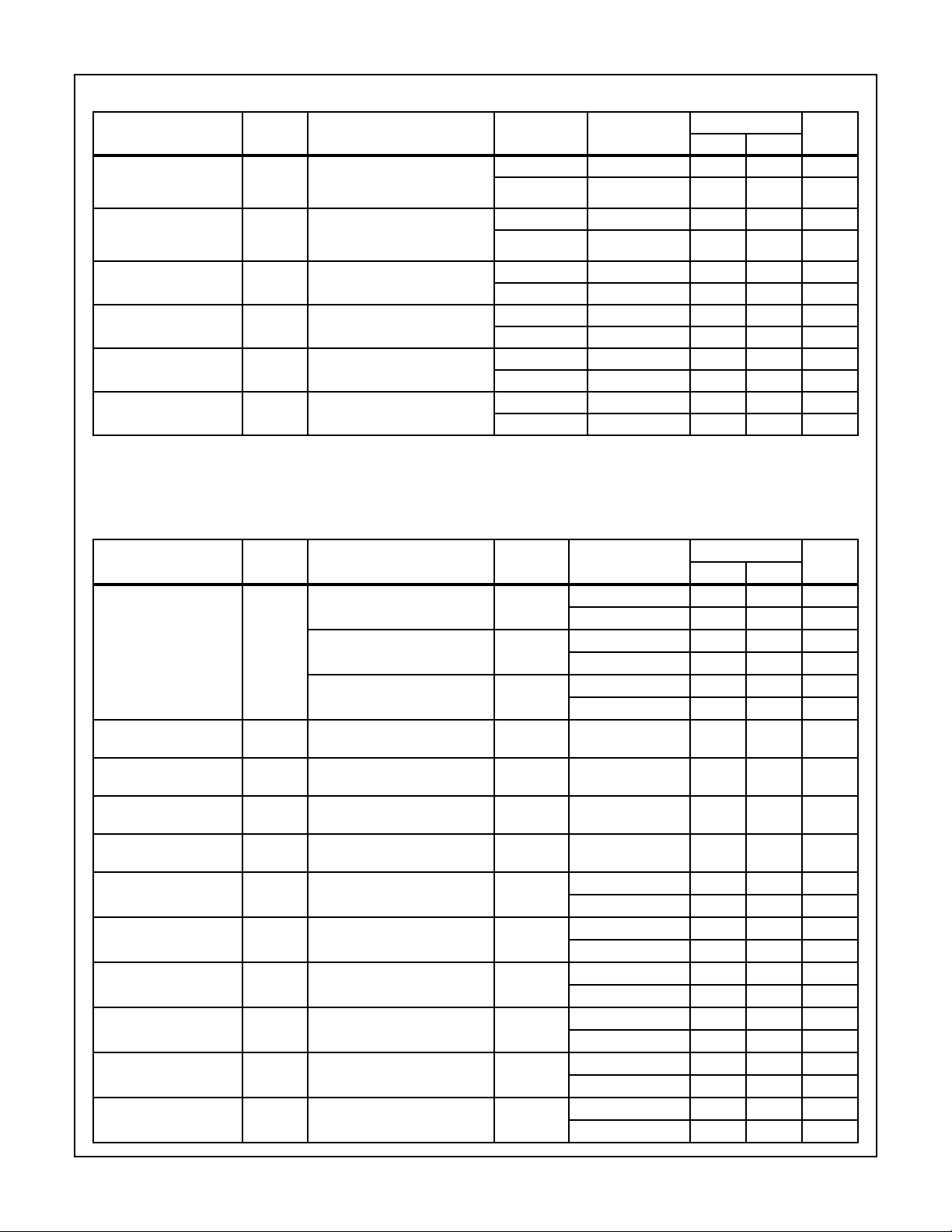
TABLE 2. AC ELECTRICAL PERFORMANCE CHARACTERISTICS
PARAMETER SYMBOL CONDITIONS (NOTE 1, 2)
Propagation Delay
Clock to Q1 8-Bypass
High
Propagation Delay
Clock to Q1 8-Bypass
Low
Propagation Delay
Clock to Q16
Propagation Delay
Reset to QN
Transition Time TTHL
Maximum Clock Input
Frequency
NOTES:
1. VDD = 5V, CL = 50pF, RL = 200K, Input TR, TF < 20ns.
2. -55oC and +125oC limits guaranteed, 100% testing being implemented.
TPHL1
TPLH1
TPHL2
TPLH2
TPHL3
TPLH3
TPHL4 VDD = 5V, VIN = VDD or GND 9 +25oC - 6000 ns
TTLH
FCL VDD = 5V, VIN = VDD or GND 9 +25oC .5 - MHz
VDD = 5V, VIN = VDD or GND 9 +25oC - 2000 ns
VDD = 5V, VIN = VDD or GND 9 +25oC - 5000 ns
VDD = 5V, VIN = VDD or GND 9 +25oC - 8000 ns
VDD = 5V, VIN = VDD or GND 9 +25oC - 200 ns
GROUP A
SUBGROUPS TEMPERATURE
10, 11 +125oC, -55oC - 2700 ns
10, 11 +125oC, -55oC - 6750 ns
10, 11 +125oC, -55oC - 10800 ns
10, 11 +125oC, -55oC - 8100 ns
10, 11 +125oC, -55oC - 270 ns
10, 11 +125oC, -55oC .37 - MHz
LIMITS
UNITSMIN MAX
TABLE 3. ELECTRICAL PERFORMANCE CHARACTERISTICS
LIMITS
PARAMETER SYMBOL CONDITIONS NOTES TEMPERATURE
o
Supply Current IDD VDD = 5V, VIN = VDD or GND 1, 2 -55
VDD = 10V, VIN = VDD or GND 1, 2 -55oC, +25oC-10µA
VDD = 15V, VIN = VDD or GND 1, 2 -55oC, +25oC-10µA
Output Voltage VOL VDD = 5V, No Load 1, 2 +25oC, +125oC, -
Output Voltage VOL VDD = 10V, No Load 1, 2 +25oC, +125oC, -
Output Voltage VOH VDD = 5V, No Load 1, 2 +25oC, +125oC, -
Output Voltage VOH VDD = 10V, No Load 1, 2 +25oC, +125oC, -
Output Current (Sink) IOL5 VDD = 5V, VOUT = 0.4V 1, 2 +125oC 0.36 - mA
Output Current (Sink) IOL10 VDD = 10V, VOUT = 0.5V 1, 2 +125oC 0.9 - mA
Output Current (Sink) IOL15 VDD = 15V, VOUT = 1.5V 1, 2 +125oC 2.4 - mA
Output Current (Source) IOH5A VDD = 5V, VOUT = 4.6V 1, 2 +125oC - -0.36 mA
Output Current (Source) IOH5B VDD = 5V, VOUT = 2.5V 1, 2 +125oC - -1.15 mA
Output Current (Source) IOH10 VDD = 10V, VOUT = 9.5V 1, 2 +125oC - -0.9 mA
C, +25oC-5µA
+125oC - 150 µA
+125oC - 300 µA
+125oC - 600 µA
-50mV
55oC
-50mV
55oC
4.95 - V
55oC
9.95 - V
55oC
-55oC 0.64 - mA
-55oC 1.6 - mA
-55oC 4.2 - mA
-55oC - -0.64 mA
-55oC - -2.0 mA
-55oC - -1.6 mA
UNITSMIN MAX
7-1238
Page 4
Specifications CD4536BMS
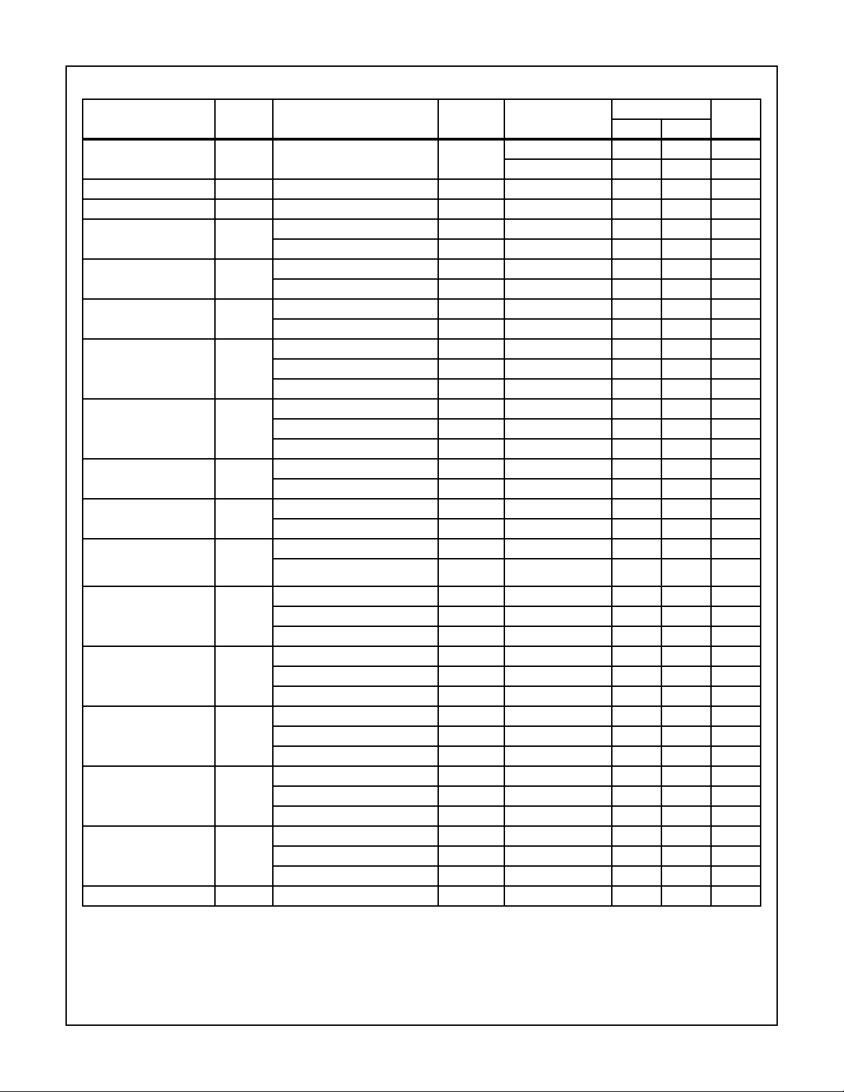
TABLE 3. ELECTRICAL PERFORMANCE CHARACTERISTICS
PARAMETER SYMBOL CONDITIONS NOTES TEMPERATURE
Output Current (Source) IOH15 VDD =15V, VOUT = 13.5V 1, 2 +125oC - -2.4 mA
Input Voltage Low VIL VDD = 10V, VOH > 9V , VOL < 1V 1, 2 +2 5oC, +125oC, -55oC- 3 V
Input Voltage High VIH VDD = 10V, VOH > 9V, VOL < 1V 1, 2 +2 5oC, +125oC, -55oC+7 - V
Propagation Delay
Clock to Q1 8-Bypass High
Propagation Delay
Clock to Q1 8-Bypass Low
Propagation Delay
Clock to Q16
Propagation Delay
Qn to Qn+1
Propagation Delay
Set to Qn
Propagation Delay
Reset to Qn
Transition Time TTHL
Maximum Clock Input
Frequency. Unlimited Input Rise or Fall Time
Minimum Clock Pulse
Width
Minimum Set Pulse Width TW VDD = 5V 1, 2, 3 +25oC - 400 ns
Minimum Reset Pulse
Width
Minimum Set Recovery
Time
Minimum Reset Recovery Time
Input Capacitance CIN Any Input 1, 2 +25oC - 7.5 pF
NOTES:
1. All voltages referenced to device GND.
2. The parameters listed on Table 3 are controlled via design or process and are not directly tested. These parameters are characterized
on initial design release and upon design changes which would affect these characteristics.
3. CL = 50pF, RL = 200K, Input TR, TF < 20ns.
TPHL1
TPLH1
TPHL2
TPLH2
TPHL3
TPLH3
TPHL
TPLH
TPLH VDD = 5V 1, 2, 3 +25oC - 600
TPHL4 VDD = 10V 1, 2, 3 +25oC - 2000 ns
TTLH
FCL VDD = 10V 1, 2, 3 +25oC 1.5 - MHz
TW VDD = 5V 1, 2, 3 +25oC - 400 ns
TW VDD = 5V 1, 2, 3 +25oC-6µs
TREM VDD = 5V 1, 2, 3 +25oC-5µs
TREM VDD = 5V 1, 2, 3 +25oC-7µs
VDD = 10V 1, 2, 3 +25oC - 1000 ns
VDD = 15V 1, 2, 3 +25oC - 700 ns
VDD = 10V 1, 2, 3 +25oC - 1600 ns
VDD = 15V 1, 2, 3 +25oC - 1200 ns
VDD = 10V 1, 2, 3 +25oC - 3000 ns
VDD = 15V 1, 2, 3 +25oC - 2000 ns
VDD = 5V 1, 2, 3 +25oC - 300
VDD = 10V 1, 2, 3 +25oC - 150
VDD = 15V 1, 2, 3 +25oC - 100
VDD = 10V 1, 2, 3 +25oC - 250
VDD = 15V 1, 2, 3 +25oC - 160
VDD = 15V 1, 2, 3 +25oC - 1500 ns
VDD = 10V 1, 2, 3 +25oC - 100 ns
VDD = 15V 1, 2, 3 +25oC - 80 ns
VDD = 15V 1, 2, 3 +25oC 2.5 - MHz
VDD = 10V 1, 2, 3 +25oC - 150 ns
VDD = 15V 1, 2, 3 +25oC - 100 ns
VDD = 10V 1, 2, 3 +25oC - 200 ns
VDD = 15V 1, 2, 3 +25oC - 120 ns
VDD = 10V 1, 2, 3 +25oC-2µs
VDD = 15V 1, 2, 3 +25oC - 1.5 µs
VDD = 10V 1, 2, 3 +25oC-2µs
VDD = 15V 1, 2, 3 +25oC - 1.6 µs
VDD = 10V 1, 2, 3 +25oC-3µs
VDD = 15V 1, 2, 3 +25oC-2µs
(Continued)
LIMITS
UNITSMIN MAX
-55oC - -4.2 mA
7-1239
Page 5

Specifications CD4536BMS
TABLE 4. POST IRRADIATION ELECTRICAL PERFORMANCE CHARACTERISTICS
LIMITS
PARAMETER SYMBOL CONDITIONS NOTES TEMPERATURE
Supply Current IDD VDD = 20V, VIN = VDD or GND 1, 4 +25oC-25µA
N Threshold Voltage VNTH VDD = 10V, ISS = -10µA 1, 4 +25oC -2.8 -0.2 V
N Threshold Voltage
Delta
P Threshold Voltage VTP VSS = 0V, IDD = 10µA 1, 4 +25oC 0.2 2.8 V
P Threshold Voltage
Delta
Functional F VDD = 18V, VIN = VDD or GND 1 +25oC VOH >
Propagation Delay Time TPHL
NOTES: 1. All voltages referenced to device GND.
2. CL = 50pF, RL = 200K, Input TR, TF < 20ns.
∆VTN VDD = 10V, ISS = -10µA 1, 4 +25oC-±1V
∆VTP VSS = 0V, IDD = 10µA 1, 4 +25oC-±1V
VOL <
VDD = 3V, VIN = VDD or GND
VDD = 5V 1, 2, 3, 4 +25oC - 1.35 x
TPLH
3. See Table 2 for +25oC limit.
4. Read and Record
TABLE 5. BURN-IN AND LIFE TEST DELTA PARAMETERS +25oC
PARAMETER SYMBOL DELTA LIMIT
Supply Current - MSI-2 IDD ± 1.0µA
Output Current (Sink) IOL5 ± 20% x Pre-Test Reading
Output Current (Source) IOH5A ± 20% x Pre-Test Reading
VDD/2
VDD/2
+25oC
Limit
UNITSMIN MAX
ns
V
TABLE 6. APPLICABLE SUBGROUPS
MIL-STD-883
CONFORMANCE GROUP
Initial Test (Pre Burn-In) 100% 5004 1, 7, 9 IDD, IOL5, IOH5A
Interim Test 1 (Post Burn-In) 100% 5004 1, 7, 9 IDD, IOL5, IOH5A
Interim Test 2 (Post Burn-In) 100% 5004 1, 7, 9 IDD, IOL5, IOH5A
PDA (Note 1) 100% 5004 1, 7, 9, Deltas
Interim Test 3 (Post Burn-In) 100% 5004 1, 7, 9 IDD, IOL5, IOH5A
PDA (Note 1) 100% 5004 1, 7, 9, Deltas
Final Test 100% 5004 2, 3, 8A, 8B, 10, 11
Group A Sample 5005 1, 2, 3, 7, 8A, 8B, 9, 10, 11
Group B Subgroup B-5 Sample 5005 1, 2, 3, 7, 8A, 8B, 9, 10, 11, Deltas Subgroups 1, 2, 3, 9, 10, 11
Subgroup B-6 Sample 5005 1, 7, 9
Group D Sample 5005 1, 2, 3, 8A, 8B, 9 Subgroups 1, 2 3
NOTE: 1. 5% Parameteric, 3% Functional; Cumulative for Static 1 and 2.
CONFORMANCE GROUPS
Group E Subgroup 2 5005 1, 7, 9 Table 4 1, 9 Table 4
METHOD GROUP A SUBGROUPS READ AND RECORD
TABLE 7. TOTAL DOSE IRRADIATION
MIL-STD-883
METHOD
PRE-IRRAD POST-IRRAD PRE-IRRAD POST-IRRAD
TEST READ AND RECORD
7-1240
Page 6

Specifications CD4536BMS
TABLE 8. BURN-IN AND IRRADIATION TEST CONNECTIONS
OSCILLATOR
FUNCTION OPEN GROUND VDD 9V ± -0.5V
Static Burn-In 1
4, 5, 13 1-3, 6-12, 14, 15 16
50kHz 25kHz
Note 1
Static Burn-In 2
Note 1
Dynamic Burn-
4, 5, 13 8 1-3, 6, 7, 9-12,
14-16
- 1, 2, 6-8, 14, 15 9-12, 16 4, 5, 13 3
In Note 1
Irradiation
Note 2
4, 5, 13 8 1-3, 6, 7, 9-12,
14-16
NOTE:
1. Each pin except VDD and GND will have a series resistor of 10K ± 5%, VDD = 18V ± 0.5V
2. Each pin except VDD and GND will have a series resistor of 47K±5%; Group E, Subgroup 2, sample size is 4 dice/wafer, 0 failures, VDD = 10V± 0.5V
Logic Diagram
6
8-BYPASS
*
VDD
*
RESET
2
RS
RT
SET
CLOCK
INH
CT
OSC
INH
IN 1
OUT 1
OUT 2
*
1
S
*
7
*
14
*
3
*
4
*
5
Q
CLDIS
CL
R
FF25
R
R
R
Q
CLEN
Q
CL
FF1 FF2 FF3 FF8
φ
D
CL
Q
Q
Q
Q
φ
CL
p
n
p
n
R
φ
Q
Q
φ
*INPUTS PROTECTED BY CMOS
PROTECTION NETWORK
VSS
A
B
C
D
E
F
FIGURE 1.
7-1241
NOTE: f ≈
1
, RS ≈ (5 → 10) x RT
3RT CT
G
Page 7

Logic Diagram (Continued)
A
B
CD4536BMS
p
n
C
D
E
F
R
CLDIS
CLQQ
FF9 FF10 FF11 FF16
9
A
G
11
10
*
*
B
*
*
12
D
C
MONO IN
R
D
CLQQ
15
*
R
φ
φ
p
n
R
Q
Q
1 OF 16 DECODER (TRANSMISSION-GATE TREE LOGIC)
φ
Q
Q
φ
VSS
P
R
Q
φ
φ
Q
FF17 FF18
N
R
φ
Q
Q
φ
R
φ
φ
FF24
DECODE
OUT
13
Q
Q
DETAIL FOR
FF3-8, 11-16, 17-24
CLEN (CLDIS FOR FF9 AND FF25)
Q
φ
p
φ
Q
VDD
N
P
P
N
N
φ
φ
φ
N
φ
φ
p
n
P
N
φ
φ
P
N
VSS
pn
N
R
R
P
P
N
R
φ
Q
e
n
f
p
f
Q
n
Q
CL
R
CLEN
Q
FF2, FF10:
CL
FF1
FF1: AS SHOWN EXCEPT Q NOT BROUGHT OUT
FF9:
SAME AS FF1 EXCEPT Q IS BROUGHT OUT AND Q, Q GO TO TGf AND TGe RESP.
DELETE TGe, TGf, AND INVf; FEED Q TO D; DELETE CLEN, CLDIS
FF25:
INVa AND INVd BECOME 2-INPUT NAND GATES, WITH ADDED INPUTS
TO TGf VSS TO TGe PREVIOUS Q INPUT; DELETE
φ
p
D
a
n
φ
φ
e
φ
Q
DETAIL FOR
FF1, FF2, FF10, FF9, FF25
R
b
φ
p
b
a
n
R
Q
D
CL
FF2, 10
φ
R
φ
p
c
n
φ
CLDIS
CL
FF9
S
R
d
φ
p
d
n
φ
QQ
Q
Q OUTPUT
R
c
CLDIS
CL
FF25
R
Q
Q
S
S; FEED Q
Q
Q
FIGURE 1. (Continued)
7-1242
Page 8

CD4536BMS
TRUTH TABLE
IN SET RESET CLOCK INH OSC INH OUT1 OUT2 DECODE OUT
0 0 0 0 No Change
0 0 0 0 Advance to Next State
X1000011
X0100010
X 0 0 1 0 No Change
0 0 0 0 X 0 1 No Change
1 0 0 0 Advance to Next State
0 = Low Level 1 = High Level X = Don’t Care
Typical Performance Characteristics
AMBIENT TEMPERATURE (TA) = +25oC
30
25
20
15
10
5
OUTPUT LOW (SINK) CURRENT (IOL) (mA)
0 5 10 15
GATE-TO-SOURCE VOLTAGE (VGS) = 15V
10V
5V
DRAIN-TO-SOURCE VOLTAGE (VDS) (V)
FIGURE 2. TYPICAL OUTPUT LOW (SINK) CURRENT
CHARACTERISTICS
DRAIN-TO-SOURCE VOLTAGE (VDS) (V)
AMBIENT TEMPERATURE (TA) = +25oC
GATE-TO-SOURCE VOLTAGE (VGS) = -5V
AMBIENT TEMPERATURE (TA) = +25oC
15.0
12.5
10.0
7.5
5.0
2.5
OUTPUT LOW (SINK) CURRENT (IOL) (mA)
0 5 10 15
GATE-TO-SOURCE VOLTAGE (VGS) = 15V
10V
5V
DRAIN-TO-SOURCE VOLTAGE (VDS) (V)
FIGURE 3. MINIMUM OUTPUT LOW (SINK) CURRENT
CHARACTERISTICS
0-5-10-15
0
-5
-10
DRAIN-TO-SOURCE VOLTAGE (VDS) (V)
AMBIENT TEMPERATURE (TA) = +25oC
GATE-TO-SOURCE VOLTAGE (VGS) = -5V
0-5-10-15
0
-5
-15
-10V
-15V
-20
-25
-30
FIGURE 4. TYPICAL OUTPUT HIGH (SOURCE) CURRENT
CHARACTERISTICS
-10V
-15V
OUTPUT HIGH (SOURCE) CURRENT (IOH) (mA)
FIGURE 5. MINIMUM OUTPUT HIGH (SOURCE) CURRENT
CHARACTERISTICS
7-1243
-10
-15
OUTPUT HIGH (SOURCE) CURRENT (IOH) (mA)
Page 9

CD4536BMS
Typical Performance Characteristics (Continued)
2
AMBIENT TEMPERATURE (TA) = +25oC
1.5
SUPPLY VOLTAGE (VDD) = 5V
1
10V
0.5
15V
PROPAGATION DELAY TIME (tPHL, tPLH) (µs)
0
0 20406080100
LOAD CAPACITANCE (CL) (pF)
FIGURE 6. TYPICAL PROPAGATION DELAY TIME AS A
FUNCTION OF LOAD CAPACITANCE
(CLOCK TO Q1, 8-BYPASS HIGH)
2
AMBIENT TEMPERATURE (TA) = +25oC
1.5
SUPPLY VOLTAGE (VDD) = 5V
1
4
AMBIENT TEMPERATURE (TA) = +25oC
3
SUPPLY VOLTAGE (VDD) = 5V
2
1
10V
15V
PROPAGATION DELAY TIME (tPHL, tPLH) (µs)
0
0 20406080100
LOAD CAPACITANCE (CL) (pF)
FIGURE 7. TYPICAL PROPAGATION DELAY TIME AS A
FUNCTION OF LOAD CAPACITANCE
(CLOCK TO Q1, 8-BYPASS LOW)
200
AMBIENT TEMPERATURE (TA) = +25oC
SUPPLY VOLTAGE (VDD) = 5V
150
100
10V
0.5
PROPAGATION DELAY TIME (tPHL, tPLH) (µs)
0
0 20406080100
LOAD CAPACITANCE (CL) (pF)
FIGURE 8. TYPICAL PROPAGATION DELAY TIME AS A
FUNCTION OF LOAD CAPACITANCE
(CLOCK TO Q16, 8-BYPASS HIGH)
60
AMBIENT TEMPERATURE (TA) = +25oC
EXTERNAL RESISTANCE (RE) = 56kΩ
50
EXTERNAL CAPACITANCE (CX) = 1000pF
40
30
RS = 0, f = 7900Hz
20
10
RS = 120kΩ, f = 5900Hz
0
FREQUENCY DEVIATION (∆f) (%)
-10
-20
579111315
6 8 10 12 14
SUPPLY VOLTAGE (VDD) (V)
FIGURE 10. TYPICAL RC OSCILLATOR FREQUENCY
DEVIATION AS A FUNCTION OF SUPPLY
VOLTAGE
10V
15V
15V
50
PROPAGATION DELAY TIME (tPHL, tPLH) (µs)
0
0 20406080100
LOAD CAPACITANCE (CL) (pF)
FIGURE 9. TYPICAL PROPAGATION DELAY TIME AS A
FUNCTION OF LOAD CAPACITANCE
(QN TO QN + 1)
3
8
10
6
4
2
2
10
8
6
4
2
10
8
6
4
2
0
8
6
4
2
-1
10
8
6
4
OSCILLATOR FREQUENCY (F) (KHz)
2
-2
10
2
10
AMBIENT TEMPERATURE (TA) = +25oC
SUPPLY VOLTAGE (VDD) = 10V
1
f =
3Rtc CT
f vs Rtc
CT = 1000pF
RS = 2Rtc
f vs CT
Rtc = 56kΩ
RS = 120kΩ
8642
3
10
8642
4
10
8642
5
10
EXTERNAL CAPACITANCE (CT) (pF)
1
10 10
EXTERNAL RESISTANCE (Rtc) (kΩ)
2
3
10
FIGURE 11. TYPICAL RC OSCILLATOR FREQUENCY
DEVIATION AS A FUNCTION OF TIME CONSTANT
RESISTANCE AND CAPACITANCE
8642
6
10
4
10
7-1244
Page 10

CD4536BMS
Typical Performance Characteristics (Continued)
10.0
Rtc = 56kΩ
RS = 0
7.5
CX = 1000pF
5.0
2.5
0
-2.5
SUPPLY VOLTAGE (VDD) = 5V
15V
10V
5V
10V
15V
-5.0
FREQUENCY DEVIATION (∆f) (%)
-7.5
-10.0
-50
0 50 100 150
AMBIENT TEMPERATURE (T
A
)oC
FIGURE 12. TYPICAL RC OSCILLATOR FREQUENCY
DEVIATION AS A FUNCTION OF AMBIENT
TEMPERATURE (RS = 0)
3
10
8
AMBIENT TEMPERATURE (TA) = +25oC
6
4
SUPPLY VOLTAGE (VDD) = 5V
2
2
10
8
6
4
2
10
PULSE WIDTH (µs)
0.1
RX = 1mΩ
8
6
4
2
100K
1
8
50K
6
4
2
10K
8642
110
8642864286428642
2
10
3
10
4
10
EXTERNAL CAPACITANCE (CX) (pF)
FIGURE 14. TYPICAL PULSE WIDTH AS A FUNCTION OF
EXTERNAL CAPACITANCE (VDD = 5V)
10.0
Rtc = 56kΩ
RE = 120kΩ
7.5
CX = 1000pF
5.0
2.5
0
SUPPLY VOLTAGE (VDD) = 5V
15V
10V
10V
15V
-2.5
-50
5V
0 50 100 150
-5.0
FREQUENCY DEVIATION (∆f) (%)
-7.5
-10.0
AMBIENT TEMPERATURE (TA)oC
FIGURE 13. TYPICAL RC OSCILLATOR FREQUENCY
DEVIATION AS A FUNCTION OF AMBIENT
TEMPERATURE (RS = 120kΩ)
3
10
8
AMBIENT TEMPERATURE (TA) = +25oC
6
4
SUPPLY VOLTAGE (VDD) = 10V
2
2
10
8
6
4
2
10
RX = 1mΩ
8
6
4
2
PULSE WIDTH (µs)
0.1
5
10
100kΩ
1
8
50kΩ
6
4
2
10kΩ
110
8642
8642864286428642
2
10
3
10
4
10
5
10
EXTERNAL CAPACITANCE (CX) (pF)
FIGURE 15. TYPICAL PULSE WIDTH AS A FUNCTION OF
EXTERNAL CAPACITANCE (VDD = 10V)
3
10
8
AMBIENT TEMPERATURE (TA) = +25oC
6
4
SUPPLY VOLTAGE (VDD) = 15V
2
2
10
8
6
4
2
10
RX = 1mΩ
8
6
4
2
PULSE WIDTH (µs)
1
100kΩ
8
6
50kΩ
4
2
0.1
10kΩ
11010210
8642
8642864286428642
3
4
10
EXTERNAL CAPACITANCE (CX) (pF)
FIGURE 16. TYPICAL PULSE WIDTH AS A FUNCTION OF
EXTERNAL CAPACITANCE (VDD = 15V)
10
AMBIENT TEMPERATURE (TA) = +25oC
200
150
SUPPLY VOLTAGE (VDD) = 5V
100
50
TRANSITION TIME (tTHL, tTLH) (ns)
5
0
0 40 60 80 10020
LOAD CAPACITANCE (CL) (pF)
FIGURE 17. TYPICAL TRANSITION TIME AS A FUNCTION OF
LOAD CAPACITANCE
7-1245
10V
15V
Page 11

CD4536BMS
Typical Performance Characteristics (Continued)
5
10
8
AMBIENT TEMPERATURE (TA) = +25oC
6
4
2
4
10
8
6
4
2
3
10
8
6
4
2
2
10
8
6
POWER DISSIPATION (PD) (µW)
4
2
10
0.1 1 10 10
SUPPLY VOLTAGE (VDD) = 15V
PULSE INPUT FREQUENCY (kHz)
FIGURE 18. TYPICAL DYNAMIC POWER DISSIPATION AS A FUNCTION OF INPUT PULSE FREQUENCY
Applications
10V
864286428642
2
5V
CL = 50pF
CL = 15pF
8642
3
10
Q1
VDD
CL
CODE OUT
÷ 8)
(CL
Q1 OUTPUT
CD4098BMS
R
>10K
9
10
11
12
1
2
6
15
14
A
B
C
D
SET
RESET
8-BYPASS
C INH
MONO IN
OSC INH
IN 1
VDD
16
OUT 1
OUT 2
DECODE
OUT
8
VSS
CX
RX
12 16
4
+TR
5
-TR
3
R
12
+TR
11
-TR
13
CD4098BMS
R
15 14 8
FIGURE 19. APPLICATION SHOWING USE OF CD4098BMS AND CD4536BMS TO GET DECODE PULSE 8 CLOCK PULSES AFTER
RESET PULSE
CLOCK
A
B
C
D
≥10kΩ
SET
RESET
8-BYPASS
C INH
MONO IN
OSC INH
IN 1
VDD
DECODE
OUT
VSS
OUT 1
OUT 2
t
CLOCK
CL
A
B
C
D
SET
RESET
R
8-BYPASS
C INH
MONO IN
OSC INH
IN 1
VDD
DECODE
OUT
VSS
OUT 1
OUT 2
t
FIGURE 20. TIME INTERV AL CONFIGURATION USING EXTER-
NAL CLOCK; SET AND CLOCK INHIBIT FUNCTIONS
FIGURE 21. TIME INTERVAL CONFIGURATION USING EXTER-
NAL CLOCK; RESET AND OUTPUT MONOSTABLE
TO ACHIEVE A PULSE OUTPUT
7-1246
Page 12

Applications (Continued)
FOR USE OF CD4098BMS
VDD
CD4536BMS
START
A
B
C
D
SET
RESET
8-BYPASS
C INH
MONO IN
OSC INH
IN 1
OUT 1
OUT 2
DECODE
OUT
VSS
RS
C
Rtc
1
Rtc C
f ≅
t
2.3
RS ≥ 2Rtc
f IN Hz,
R IN Ω,
C IN F
FIGURE 22. TIME INTERVAL CONFIGURATION USING ON-
CHIP RC OSCILLATOR AND RESET INPUT
TO INITIATE TIME INTERVAL
DECODE OUT SELECTION TABLE
DCBA
0
0
0
0
0
0
0
1
0
0
1
0
0
0
1
1
0
1
0
0
0
1
0
1
0
1
1
0
0
1
1
1
1
0
0
0
1
0
0
1
1
0
1
0
1
0
1
1
1
1
0
0
1
1
0
1
1
1
1
0
1
1
1
1
0 = Low Level 1 = High Level
3µs MIN
NOTE:
SHADED PULSE REPRESENTS DECODE OUTPUT
IN MONOSTABLE MODE. IF AN OUTPUT PULSE
IS REQUIRED 1 FULL COUNTDOWN AFTER
REMOVAL OF RESET PULSE, SEE FIGURE 19
CLOCK
DCBA
÷2)
0000 (
0001 (÷4)
0010 (
÷8)
R
FIGURE 23. TIMING DIAGRAM
NUMBER OF STAGES IN DIVIDER CHAIN
8-BYPASS = 0 8-BYPASS = 1
9
10
11
12
13
14
15
16
17
18
19
20
21
22
23
24
1
2
3
4
5
6
7
8
9
10
11
12
13
14
15
16
Functional Block Diagram
1
SET
OSC
OUT 1
OUT 2
IN
2
14
3
4
5
7
OSC INHIBIT
LOGIC
CLOCK INHIBIT
VSS = 8
VDD = 16
RESET
INHIBIT
CLOCK
INHIBIT
LOGIC
STAGES
1-8
FIGURE 24.
7-1247
8-BYPASS
8-BYPASS
BINARY
SELECT
6
LOGIC
MONO IN
STAGES 9-24
Q9 - - - Q24
9
A
10
B
11
C
D
DECODER
12
15
13
DECODE
OUT
Page 13

CD4536BMS
FUNCTIONAL TEST SEQUENCE
INPUTS OUTPUTS COMMENTS
DECODE OUT
IN 1 SET RESET 8-BYPASS
1111 0Counter is in three 8-stage section in parallel
0111 0First “1” to “0” transition of clock
1
0
-
-
0111 1The 255 “1” to “0” transition
0000 1Counter converted back to 24 stages in series
1000 1In1 Switches to a “1”
0000 0Counter Ripples from an all “1” state to an all
111
Q1 THRU 24
ALL 24 STEPS ARE IN RESET MODE1011 0
mode
255 “1” to “0” transitions are clocked in the
counter
mode.
Set and Reset must be connected together
and simultaneously go from “1” to “0”
“0” state
Functional Test Sequence
Test Function has been included for the reduction of test
time required to exercise all 24 counter stages. This test
function divides the counter into three 8-stage sections and
255 counts are loaded in each of the 8-stage sections in par-
Chip Dimensions and Pad Layout
INTERSIL
allel. All flip-flops are now at a “1”. The counter is now
returned to the normal 24 steps in series configuration. One
more pulse is entered into In1 which will cause the counter
to ripple from an all “1” state to an all “0” state.
Dimensions in parenthesis are in millimeters and are derived from
the basic inch dimensions as indicated. Grid graduations are in mils
-3
(10
inch).
METALLIZATION: Thickness: 11kÅ− 14kÅ, AL.
PASSIVATION: 10.4kÅ - 15.6kÅ, Silane
BOND PADS: 0.004 inches X 0.004 inches MIN
DIE THICKNESS: 0.0198 inches - 0.0218 inches
All Intersil semiconductor products are manufactured, assembled and tested under ISO9000 quality systems certification.
Intersil products are sold by description only. Intersil Corporation reserves the right to make changes in circuit design and/or specifications at any time without
notice. Accordingly, the reader is cautioned to verify that data sheets are current before placing orders. Information furnished by Intersil is believed to be accurate
and reliable. However, no responsibility is assumed by Intersil or its subsidiaries for its use; nor for any infringements of patents or other rights of third parties which
may result from its use. No license is granted by implication or otherwise under any patent or patent rights of Intersil or its subsidiaries.
For information regarding Intersil Corporation and its products, see web site http://www.intersil.com
1248
 Loading...