

Page 1
TL/F/5998
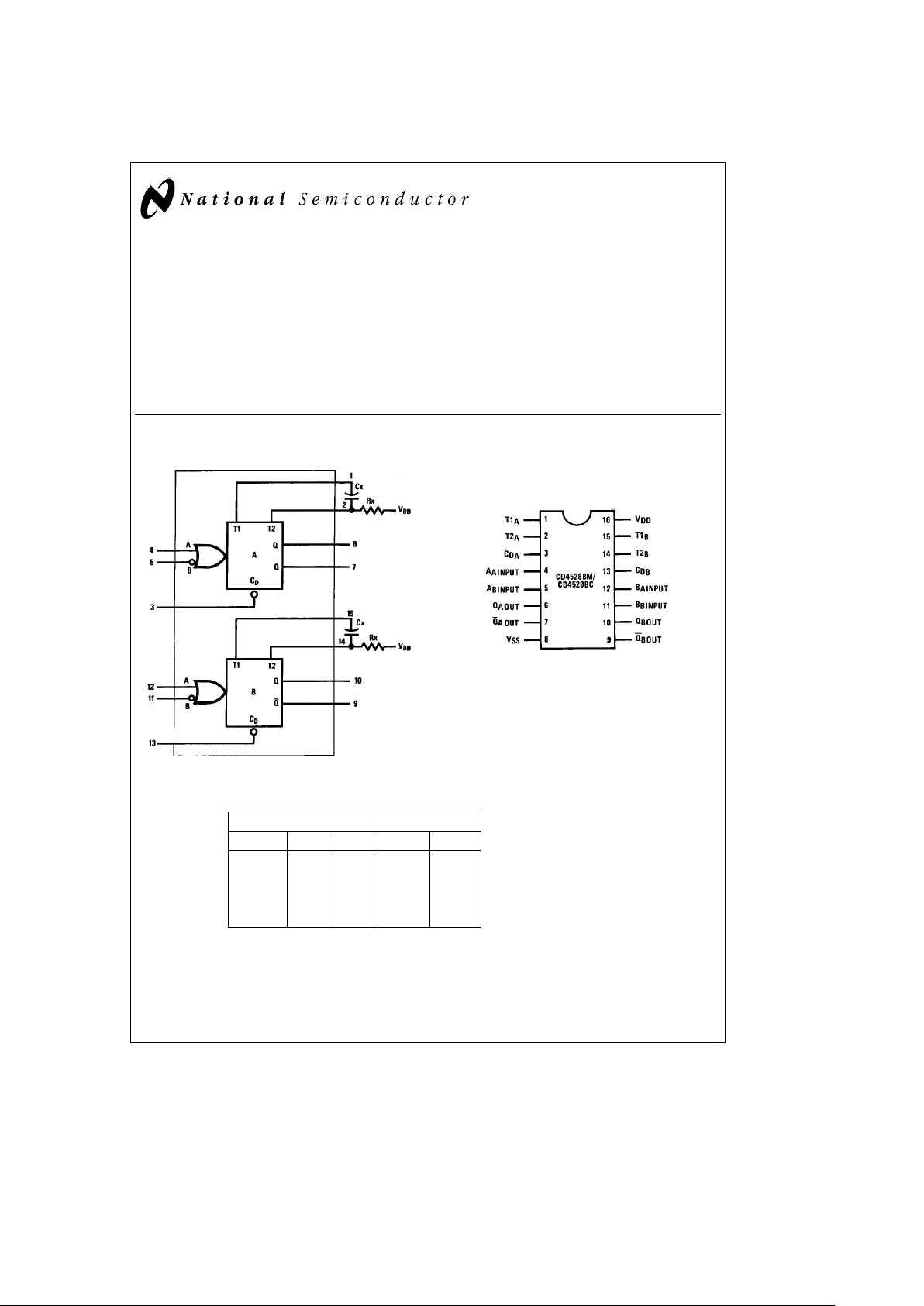
CD4528BM/CD4528BC Dual Monostable Multivibrator
February 1988
CD4528BM/CD4528BC Dual Monostable Multivibrator
General Description
The CD4528B is a dual monostable multivibrator. Each device is retriggerable and resettable. Triggering can occur
from either the rising or falling edge of an input pulse, resulting in an output pulse over a wide range of widths. Pulse
duration and accuracy are determined by external timing
components Rx and Cx.
Features
Y
Wide supply voltage range 3.0V to 18V
Y
Separate reset available
Y
Quiescent currente5.0 nA/package (typ.) at 5.0 V
DC
Y
Diode protection on all inputs
Y
Triggerable from leading or trailing edge pulse
Y
Capable of driving two low-power TTL loads or one
low-power Schottky TTL load over the rated temperature range
Connection Diagrams
TL/F/5998– 1
Dual-In-Line Package
TL/F/5998– 2
Top View
Order Number CD4528B
Truth Table
Inputs Outputs
HeHigh Level
Clear A B Q Q
LeLow Level
LXXLH
u
e
Transition from Low to High
XHXLH
v
e
Transition from High to Low
XXLLH
É
e
One High Level Pulse
HL
v
Éß
ß
e
One Low Level Pulse
H
u
H Éß
X
e
Irrelevant
C
1995 National Semiconductor Corporation RRD-B30M105/Printed in U. S. A.
Page 2
Absolute Maximum Ratings (Notes1&2)
If Military/Aerospace specified devices are required,
please contact the National Semiconductor Sales
Office/Distributors for availability and specifications.
DC Supply Voltage (V
DD
)
b
0.5 VDCtoa18 V
DC
Input Voltage, All Inputs (VIN)b0.5 VDCto V
DD
a
0.5 V
DC
Storage Temperature
Range (T
S
)
b
65§Ctoa150§C
Power Dissipation (P
D
)
Dual-In-Line 700 mW
Small Outline 500 mW
Lead Temperature (T
L
)
(Soldering, 10 seconds) 260
§
C
Recommended Operating
Conditions
(Note 2)
DC Supply Voltage (VDD) 3Vto15V
Input Voltage (VIN) 0VtoVDDV
DC
Operating Temperature Range (TA)
CD4528BM
b
55§Ctoa125§C
CD4528BC
b
40§Ctoa85§C
DC Electrical Characteristics CD4528BM (Note 2)
Symbol Parameter Conditions
b
55§C
a
25§C
a
125§C
Units
Min Max Min Typ Max Min Max
I
DD
Quiescent Device Current V
DD
e
5V 5 0.005 5 150 mA
V
DD
e
10V 10 0.010 10 300 mA
V
DD
e
15V 20 0.015 20 600 mA
V
OL
Low Level Output Voltage V
DD
e
5V 0.05 0.05 0.05 V
V
DD
e
10V 0.05 0.05 0.05 V
V
DD
e
15V 0.05 0.05 0.05 V
V
OH
High Level Output Voltage V
DD
e
5V 4.95 4.95 5.0 4.95 V
V
DD
e
10V 9.95 9.95 10.0 9.95 V
V
DD
e
15V 14.95 14.95 15.0 14.95 V
V
IL
Low Level Input Voltage V
DD
e
5V, V
O
e
0.5V or 4.5V 1.5 2.25 1.5 1.5 V
V
DD
e
10V, V
O
e
1V or 9V 3.0 4.50 3.0 3.0 V
V
DD
e
15V, V
O
e
1.5V or 13.5V 4.0 6.75 4.0 4.0 V
V
IH
High Level Input Voltage V
DD
e
5V, V
O
e
0.5V or 4.5V 3.5 3.5 2.75 3.5 V
V
DD
e
10V, V
O
e
1V or 9V 7.0 7.0 5.50 7.0 V
V
DD
e
15V, V
O
e
1.5V or 13.5V 11.0 11.0 8.25 11.0 V
I
OL
Low Level Output Current V
DD
e
5V, V
O
e
0.4V 0.64 0.51 0.88 0.36 mA
(Note 3) V
DD
e
10V, V
O
e
0.5V 1.6 1.3 2.25 0.9 mA
V
DD
e
15V, V
O
e
1.5V 4.2 3.4 8.8 2.4 mA
I
OH
High Level Output Current V
DD
e
5V, V
O
e
4.6V
b
0.25
b
0.2b0.36
b
0.14 mA
(Note 3) V
DD
e
10V, V
O
e
9.5V
b
0.62
b
0.5b0.9
b
0.35 mA
V
DD
e
15V, V
O
e
13.5V
b
1.8
b
1.5b3.5
b
1.1 mA
I
IN
Input Current V
DD
e
15V, V
IN
e
0V
b
0.1
b
10
b
5
b
0.1
b
1.0 mA
V
DD
e
15V, V
IN
e
15V 0.1 10
b
5
0.1 1.0 mA
Note 1: ‘‘Absolute Maximum Ratings’’ are those values beyond which the safety of the device cannot be guaranteed. Except for ‘‘Operating Temperature Range’’,
they are not meant to imply that the devices should be operated at these limits. The table of ‘‘Electrical Characteristics’’ provides conditions for actual device
operation.
Note 2: V
SS
e
0V unless otherwise specified.
Note 3: I
OH
and IOLare tested one output at a time.
2
Page 3
DC Electrical Characteristics CD4528BC (Note 2)
Symbol Parameter Conditions
b
40§C
a
25§C
a
85§C
Units
Min Max Min Typ Max Min Max
I
DD
Quiescent Device Current V
DD
e
5V 20 0.005 20 150 mA
V
DD
e
10V 40 0.010 40 300 mA
V
DD
e
15V 80 0.015 80 600 mA
V
OL
Low Level Output Voltage V
DD
e
5V 0.05 0.05 0.05 V
V
DD
e
10V 0.05 0.05 0.05 V
V
DD
e
15V 0.05 0.05 0.05 V
V
OH
High Level Output Voltage V
DD
e
5V 4.95 4.95 5.0 4.95 V
V
DD
e
10V 9.95 9.95 10.0 9.95 V
V
DD
e
15V 14.95 14.95 15.0 14.95 V
V
IL
Low Level Input Voltage V
DD
e
5V, V
O
e
0.5V or 4.5V 1.5 2.25 1.5 1.5 V
V
DD
e
10V, V
O
e
1V or 9V 3.0 4.50 3.0 3.0 V
V
DD
e
15V, V
O
e
1.5V or 13.5V 4.0 6.75 4.0 4.0 V
V
IH
High Level Input Voltage V
DD
e
5V, V
O
e
0.5V or 4.5V 3.5 3.5 2.75 3.5 V
V
DD
e
10V, V
O
e
1V or 9V 7.0 7.0 5.50 7.0 V
V
DD
e
15V, V
O
e
1.5V or 13.5V 11.0 11.0 8.25 11.0 V
I
OL
Low Level Output Current V
DD
e
5V, V
O
e
0.4V 0.52 0.44 0.88 0.36 mA
(Note 3) V
DD
e
10V, V
O
e
0.5V 1.3 1.1 2.25 0.9 mA
V
DD
e
15V, V
O
e
1.5V 3.6 3.0 8.8 2.4 mA
I
OH
High Level Output Current V
DD
e
5V, V
O
e
4.6V
b
0.2
b
0.16b0.36
b
0.12 mA
(Note 3) V
DD
e
10V, V
O
e
9.5V
b
0.5
b
0.4b0.9
b
0.3 mA
V
DD
e
15V, V
O
e
13.5V
b
1.4
b
1.2b3.5
b
1.0 mA
I
IN
Input Current V
DD
e
15V, V
IN
e
0V
b
0.3
b
10
b
5
b
0.3
b
1.0 mA
V
DD
e
15V, V
IN
e
15V 0.3 10
b
5
0.3 1.0 mA
Note 1: ‘‘Absolute Maximum Ratings’’ are those values beyond which the safety of the device cannot be guaranteed. Except for ‘‘Operating Temperature Range’’,
they are not meant to imply that the devices should be operated at these limits. The table of ‘‘Electrical Characteristics’’ provides conditions for actual device
operation.
Note 2: V
SS
e
0V unless otherwise specified.
Note 3: I
OH
and IOLare tested one output at a time.
3
Page 4

AC Electrical Characteristics* CD4528BM
T
A
e
25§C, C
L
e
50 pF, R
L
e
200 kX, Input t
r
e
t
f
e
20 ns, unless otherwise specified
Parameter Conditions Min Typ Max Units
Output Rise Time t
r
e
(3.0 ns/pF) C
L
a
30 ns, V
DD
e
5.0V 180 400 ns
t
r
e
(1.5 ns/pF) C
L
a
15 ns, V
DD
e
10.0V 90 200 ns
t
r
e
(1.1 ns/pF) C
L
a
10 ns, V
DD
e
15.0V 65 160 ns
Output Fall Time t
f
e
(1.5 ns/pF) C
L
a
25 ns, V
DD
e
5.0V 100 200 ns
t
f
e
(0.75 ns/pF) C
L
a
12.5 ns, V
DD
e
10V 50 100 ns
t
f
e
(0.55 ns/pF) C
L
a
9.5 ns, V
DD
e
15.0V 35 80 ns
Turn-Off, Turn-On Delay t
PLH,tPHL
e
(1.7 ns/pF) C
L
a
240 ns, V
DD
e
5.0V 230 500 ns
AorBtoQorQ
t
PLH,tPHL
e
(0.66 ns/pF) C
L
a
8 ns, V
DD
e
10.0V 100 250 ns
Cx
e
15 pF, Rxe5.0 kX t
PLH,tPHL
e
(0.5 ns/pF) C
L
a
65 ns, V
DD
e
15.0V 65 150 ns
Turn-Off, Turn-On Delay t
PLH,tPHL
e
(1.7 ns/pF) C
L
a
620 ns, V
DD
e
5.0V 230 500 ns
AorBtoQorQ
t
PLH,tPHL
e
(0.66 ns/pF) C
L
a
257 ns, V
DD
e
10.0V 100 250 ns
Cx
e
100 pF, Rxe10 kX t
PLH,tPHL
e
(0.5 ns/pF) C
L
a
185 ns, V
DD
e
15.0V 65 150 ns
Minimum Input Pulse Width V
DD
e
5.0V 60 150 ns
AorB V
DD
e
10.0V 20 50 ns
Cx
e
15 pF, Rxe5.0 kX V
DD
e
15V 20 50 ns
Cxe1000 pF, Rxe10 kX V
DD
e
5.0V 60 150 ns
V
DD
e
10.0V 20 50 ns
V
DD
e
15.0V 20 50 ns
Output Pulse Width Q or Q V
DD
e
5.0V 550 ns
For Cx
k
0.01 mF (See Graph
V
DD
e
10.0V 350 ns
for Appropriate V
DD
Level)
Cx
e
15 pF, Rxe5.0 kX V
DD
e
15.0V 300 ns
For Cxl0.01 mF Use V
DD
e
5.0V 15 29 45 ms
PW
out
e
0.2 Rx Cx In[V
DD
b
V
SS
]
V
DD
e
10.0V 10 37 90 ms
Cx
e
10,000 pF, Rxe10 kX V
DD
e
15.0V 15 42 95 ms
Pulse Width Match between Circuits V
DD
e
5.0V 6 25 %
in the Same Package V
DD
e
10.0V 8 35 %
Cx
e
10,000 pF, Rxe10 kX V
DD
e
15.0V 8 35 %
Reset Propagation Delay, V
DD
e
5.0V 325 600 ns
t
PLH,tPHL
V
DD
e
10.0V 90 225 ns
Cx
e
15 pF, Rxe5.0 kX V
DD
e
15.0V 60 170 ns
Cxe1000 pF, Rxe10 kX V
DD
e
5.0V 7.0 ms
V
DD
e
10.0V 6.7 ms
V
DD
e
15.0V 6.7 ms
Minimum Retrigger Time V
DD
e
5.0V 0 ns
Cx
e
15 pF, Rxe5.0 kX V
DD
e
10.0V 0 ns
V
DD
e
15.0V 0 ns
Cx
e
1000 pF, Rxe10 kX V
DD
e
5.0V 0 ns
V
DD
e
10.0V 0 ns
V
DD
e
15.0V 0 ns
*AC parameters are guaranteed by DC correlated testing.
4
Page 5

Logic Diagrams ((/2 of Device Shown)
Note: Externally ground pins 1 and 15 to pin 8. TL/F/5998– 3
TL/F/5998– 4
TL/F/5998– 10
Duty Cyclee50%
FIGURE 1. Power Dissipation Test Circuit and Waveforms
TL/F/5998– 5
Input Connections
Characteristics C
D
AB
t
PLH,tPHL,tr,tf
,
V
DD
PG1 V
DD
PW
out
,PW
in
t
PLH,tPHL,tr,tf
,
V
DD
V
SS
PG2
PW
out
,PW
in
t
PLH(R),tPHL(R)
,PW
in
PG3 PG1 PG2
*Includes capacitance of probes, wir-
ing, and fixture parasitic.
Note: AC test waveforms for PG1,
PG2, and PG3 on next page.
TL/F/5998– 6
FIGURE 2. AC Test Circuit
5
Page 6

Logic Diagrams ((/2 of Device Shown) (Continued)
TL/F/5998– 7
FIGURE 3. AC Test Waveforms
TL/F/5998– 8
FIGURE 4. Normalized Pulse Width vs Temperature
TL/F/5998– 9
FIGURE 5. Pulse Width vs Cx
6
Page 7

Physical Dimensions inches (millimeters)
Ceramic Dual-In-Line Package (J)
Order Number CD4528BMJ or CD4528BCJ
NS Package Number J16A
7
Page 8

CD4528BM/CD4528BC Dual Monostable Multivibrator
Physical Dimensions inches (millimeters) (Continued)
Molded Dual-In-Line Package (N)
Order Number CD4528BMN or CD4528BCN
NS Package Number N16E
LIFE SUPPORT POLICY
NATIONAL’S PRODUCTS ARE NOT AUTHORIZED FOR USE AS CRITICAL COMPONENTS IN LIFE SUPPORT
DEVICES OR SYSTEMS WITHOUT THE EXPRESS WRITTEN APPROVAL OF THE PRESIDENT OF NATIONAL
SEMICONDUCTOR CORPORATION. As used herein:
1. Life support devices or systems are devices or 2. A critical component is any component of a life
systems which, (a) are intended for surgical implant support device or system whose failure to perform can
into the body, or (b) support or sustain life, and whose be reasonably expected to cause the failure of the life
failure to perform, when properly used in accordance support device or system, or to affect its safety or
with instructions for use provided in the labeling, can effectiveness.
be reasonably expected to result in a significant injury
to the user.
National Semiconductor National Semiconductor National Semiconductor National Semiconductor
Corporation Europe Hong Kong Ltd. Japan Ltd.
1111 West Bardin Road Fax: (
a
49) 0-180-530 85 86 13th Floor, Straight Block, Tel: 81-043-299-2309
Arlington, TX 76017 Email: cnjwge@tevm2.nsc.com Ocean Centre, 5 Canton Rd. Fax: 81-043-299-2408
Tel: 1(800) 272-9959 Deutsch Tel: (
a
49) 0-180-530 85 85 Tsimshatsui, Kowloon
Fax: 1(800) 737-7018 English Tel: (
a
49) 0-180-532 78 32 Hong Kong
Fran3ais Tel: (
a
49) 0-180-532 93 58 Tel: (852) 2737-1600
Italiano Tel: (
a
49) 0-180-534 16 80 Fax: (852) 2736-9960
National does not assume any responsibility for use of any circuitry described, no circuit patent licenses are implied and National reserves the right at any time without notice to change said circuitry and specifications.
 Loading...