

Page 1
© 2000 Fairchild Semiconductor Corporation DS005998 www.fairchildsemi.com
October 1987
Revised August 2000
CD4528BC Dual Monostable Multivibrator
CD4528BC
Dual Monostable Multivibrator
General Description
The CD4528B is a dual monostable multivibrator. Each
device is retriggerable and resettable. Triggering can occur
from either the rising or falling edge of an input pulse,
resulting in an output p ulse over a wide range of wi dths.
Pulse duration and accurac y are determined by external
timing components Rx and Cx.
Features
■ Wide supply voltage range: 3.0V to 18V
■ Separate reset available
■ Quiescent current
= 5.0 nA/package (typ.) at 5.0 V
DC
■ Diode protection on all inputs
■ Triggerable from leading or trailing edge pulse
■ Capable of driving two low- powe r TTL loa ds or one low -
power Schottky TTL load over the rated temperature
range
Ordering Code:
Devices also availab le in Tape and Reel. Specify by appending th e s uffix let t er “X” to the ordering code.
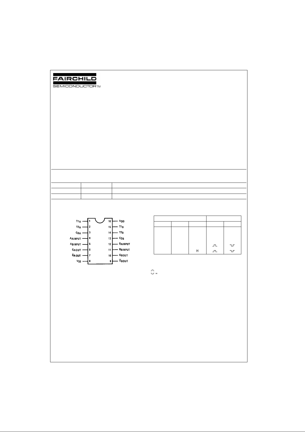
Connection Diagram
Top View
Truth Table
H = HIGH Level
L = LOW Level
↑ = Transition from LOW-to-HIGH
↓ = Transition from HIGH -t o-LOW
= One HIGH Level Pulse
= One LOW Level Pu ls e
X = Irrelevant
Order Number Package Number Package Description
CD4528BCM M16A 16-Lead Small Outline Integrated Circuit (SOIC), JEDEC MS-012, 0.150 Narrow
CD4528BCN N16E 16-Lead Plastic Dual-In-Line Package (PDIP), JEDEC MS-001, 0.300 Wide
Inputs Outputs
Clear A B Q Q
LXXLH
XHXLH
XXLLH
HL
↓
H ↑ H
Page 2
www.fairchildsemi.com 2
CD4528BC
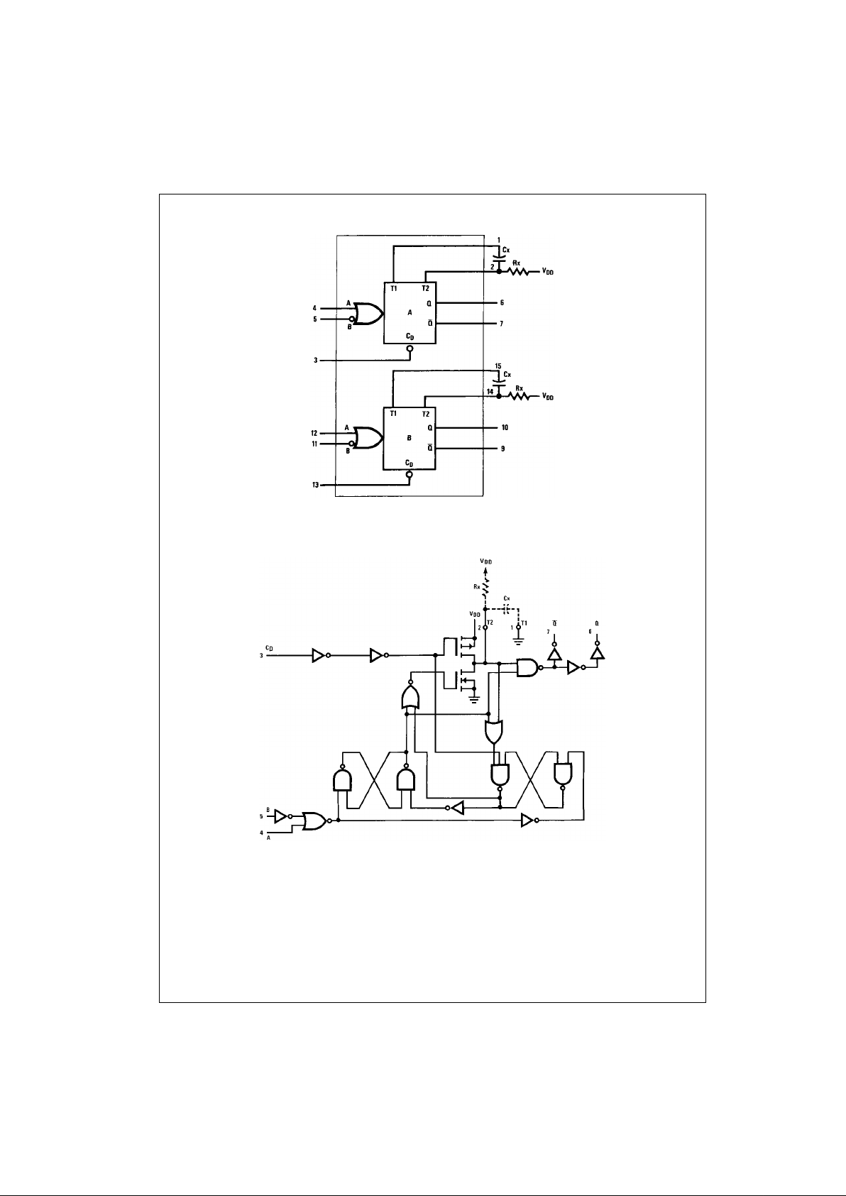
Block Diagram
Logic Diagram
(½ of Device Show n)
Note: Externally ground pins 1 and 15 to pin 8.
Page 3
3 www.fairchildsemi.com
CD4528BC
Absolute Maximum Ratings(Note 1)
(Note 2)
Recommended Operating
Conditions
(Note 2)
Note 1: “Absolute Maximum Ratings” are those values bey ond which the
safety of the device cannot be guaranteed. Except for “Operating Temperature Range”, they are not m eant to i mply th at the devices shou ld be op erated at these limits. The table of “Electrical Characteristics” provides
conditions for actual device operation.
Note 2: V
SS
= 0V unless otherw is e s pecified.
DC Electrical Characteristics (Note 3)
Note 3: VSS = 0V unless otherwise specified.
Note 4: I
OH
and IOL are tested one out put at a time.
DC Supply Voltage (VDD) −0.5 VDC to +18 V
DC
Input Voltage, All Inputs (VIN) −0.5 VDC to VDD +0.5 V
DC
Storage Temperature Range (TS) −65°C to +150°C
Power Dissipation (P
D
)
Dual-In-Line 700 mW
Small Outline 500 mW
Lead Temperature (T
L
)
(Soldering, 10 seconds) 260
°C
DC Supply Voltage (V
DD
) 3V to 15V
Input Voltage (V
IN
) 0V to VDD V
DC
Operating Temperature Range (TA) −40°C to +85°C
Symbol Parameter Conditions
−40°C +25°C +85°C
Units
Min Max Min Typ Max Min Max
I
DD
Quiescent Device Current VDD = 5V 20 0.005 20 150 µA
V
DD
= 10V 40 0.010 40 300 µA
VDD = 15V 80 0.015 80 600 µA
V
OL
LOW Level Output Voltage VDD = 5V 0.05 0.05 0.05 V
V
DD
= 10V 0.05 0.05 0.05 V
VDD = 15V 0.05 0.05 0.05 V
V
OH
HIGH Level Output Voltage VDD = 5V 4.95 4.95 5.0 4.95 V
V
DD
= 10V 9.959.9510.09.95 V
VDD = 15V 14.95 14.95 15.0 14.95 V
V
IL
LOW Level Input Voltage VDD = 5V, VO = 0.5V or 4.5V 1.5 2.25 1.5 1.5 V
V
DD
= 10V, VO = 1V or 9V 3.0 4.50 3.0 3.0 V
VDD = 15V, VO = 1.5V or 13.5V 4.0 6.75 4.0 4.0 V
V
IH
HIGH Level Input Voltage VDD = 5V, VO = 0.5V or 4.5V 3.5 3.5 2.75 3.5 V
V
DD
= 10V, VO = 1V or 9V 7.0 7.0 5.50 7.0 V
VDD = 15V, VO = 1.5V or 13.5V 11.0 11.0 8.25 11.0 V
I
OL
LOW Level Output Current VDD = 5V, VO = 0.4V 0.52 0.44 0.88 0.36 mA
(Note 4) V
DD
= 10V, VO = 0.5V 1.3 1.1 2.25 0.9 mA
VDD = 15V, VO = 1.5V 3.6 3.0 8.8 2.4 mA
I
OH
HIGH Level Output Current VDD = 5V, VO = 4.6V −0.2 −0.16 −0.36 −0.12 mA
(Note 4) V
DD
= 10V, VO = 9.5V −0.5 −0.4 −0.9 −0.3 mA
VDD = 15V, VO = 13.5V −1.4 −1.2 −3.5 −1.0 mA
I
IN
Input Current VDD = 15V, VIN = 0V −0.3 −10−5−0.3 −1.0 µA
V
DD
= 15V, VIN = 15V 0.3 10−50.3 1.0 µA
Page 4

www.fairchildsemi.com 4
CD4528BC
AC Electrical Characteristics (Note 5)
T
A
= 25°C, CL = 50 pF, RL = 200 kΩ, Input tr = t
f
= 20 ns, unless otherwise specified
Note 5: AC parameters are gu aranteed by DC correlat ed t es t ing.
Symbol Parameter Conditions Min Typ Max Units
t
r
Output Rise Time tr = (3.0 ns/pF) CL + 30 ns, VDD = 5.0V 180 400 ns
tr = (1.5 ns/pF) CL + 15 ns, VDD = 10.0V 90 200 ns
t
r
= (1.1 ns/pF) CL + 10 ns, VDD = 15.0V 65 160 ns
t
f
Output Fall Time tf = (1.5 ns/pF) CL + 25 ns, VDD = 5.0V 100 200 ns
tf = (0.75 ns/pF) CL + 12.5 ns, VDD = 10V 50 100 ns
t
f
= (0.55 ns/pF) CL + 9.5 ns, VDD = 15.0V 35 80 ns
t
PLH
Turn-Off, Turn-On Delay t
PLH
, t
PHL
= (1.7 ns/pF) CL + 240 ns, VDD = 5.0V 230 500 ns
t
PHL
A or B to Q or Q t
PLH
, t
PHL
= (0.66 ns/pF) CL + 8 ns, VDD = 10.0V 100 250 ns
Cx = 15 pF, Rx = 5.0 kΩ t
PLH
, t
PHL
= (0.5 ns/pF) CL + 65 ns, VDD = 15.0V 65 150 ns
Turn-Off, Turn-On Delay t
PLH
, t
PHL
= (1.7 ns/pF) CL + 620 ns, VDD = 5.0V 230 500 ns
A or B to Q or Q t
PLH
, t
PHL
= (0.66 ns/pF) CL + 257 ns, VDD = 10.0V 100 250 ns
Cx = 100 pF, Rx = 10 kΩ t
PLH
, t
PHL
= (0.5 ns/pF) CL + 185 ns, VDD = 15.0V 65 150 ns
t
WL
Minimum Input Pulse Width VDD = 5.0V 60 150 ns
t
WH
A or B VDD = 10.0V 20 50 ns
Cx = 15 pF, Rx = 5.0 kΩ VDD = 15V 20 50 ns
Cx = 1000 pF , Rx = 10 kΩ VDD = 5.0V 60 150 ns
VDD = 10.0V 20 50 ns
VDD = 15.0V 20 50 ns
PW
OUT
Output Pulse Width Q or Q VDD = 5.0V 550 ns
For Cx < 0.01 µF (See Graph
VDD = 10.0V 350 ns
for Appropriate VDD Level)
Cx = 15 pF, Rx = 5.0 kΩ VDD = 15.0V 300 ns
For Cx > 0.01 µF Use VDD = 5.0V 15 29 45 µs
PW
out
= 0.2 Rx Cx In [VDD − VSS]VDD = 10.0V 103790µs
Cx = 10,000 pF, Rx = 10 kΩ VDD = 15.0V 154295µs
t
PLH
Reset Propagation Delay, VDD = 5.0V 325 600 ns
t
PHL
t
PLH
, t
PHL
VDD = 10.0V 90 225 ns
Cx = 15 pF, Rx = 5.0 kΩ VDD = 15.0V 60 170 ns
Cx = 1000 pF , Rx = 10 kΩ V
DD
= 5.0V 7.0 µs
V
DD
= 10.0V 6.7 µs
VDD = 15.0V 6.7 µs
t
RR
Minimum Retrigger Time VDD = 5.0V 0 ns
Cx = 15 pF, Rx = 5.0 kΩ VDD = 10.0V 0 ns
VDD = 15.0V 0 ns
Cx = 1000 pF , Rx = 10 kΩ V
DD
= 5.0V 0 ns
V
DD
= 10.0V 0 ns
VDD = 15.0V 0 ns
Pulse Width Match between Circuits VDD = 5.0V 6 25 %
in the Same Package VDD = 10.0V 8 35 %
Cx = 10,000 pF, Rx = 10 kΩ VDD = 15.0V 8 35 %
Page 5

5 www.fairchildsemi.com
CD4528BC
Pulse Widths
FIGURE 1. Pulse Width vs Cx
FIGURE 2. Normalized Pulse Width vs Temperature
Page 6

www.fairchildsemi.com 6
CD4528BC
AC Test Circuits and Waveforms
Duty Cycle = 50%
FIGURE 3. Power Dissipation Test Circuit and Waveforms
*Includes capac ita nc e of probes, wiring, and f ix tu re parasitic.
Note: AC test waveforms for PG1, PG2, and PG3 in Figure 4.
Input Connections
FIGURE 4. AC Test Circuit
Characteristics C
D
AB
t
PLH
, t
PHL
, tr, tf,VDDPG1 V
DD
PW
out
, PW
in
t
PLH
, t
PHL
, tr, tf,VDDV
SS
PG2
PW
out
, PW
in
t
PLH(R)
, t
PHL(R)
, PW
in
PG3 PG1 PG2
Page 7

7 www.fairchildsemi.com
CD4528BC
AC Test Circuits and Wave forms (Continued)
FIGURE 5. AC Test Waveforms
Page 8
www.fairchildsemi.com 8
CD4528BC
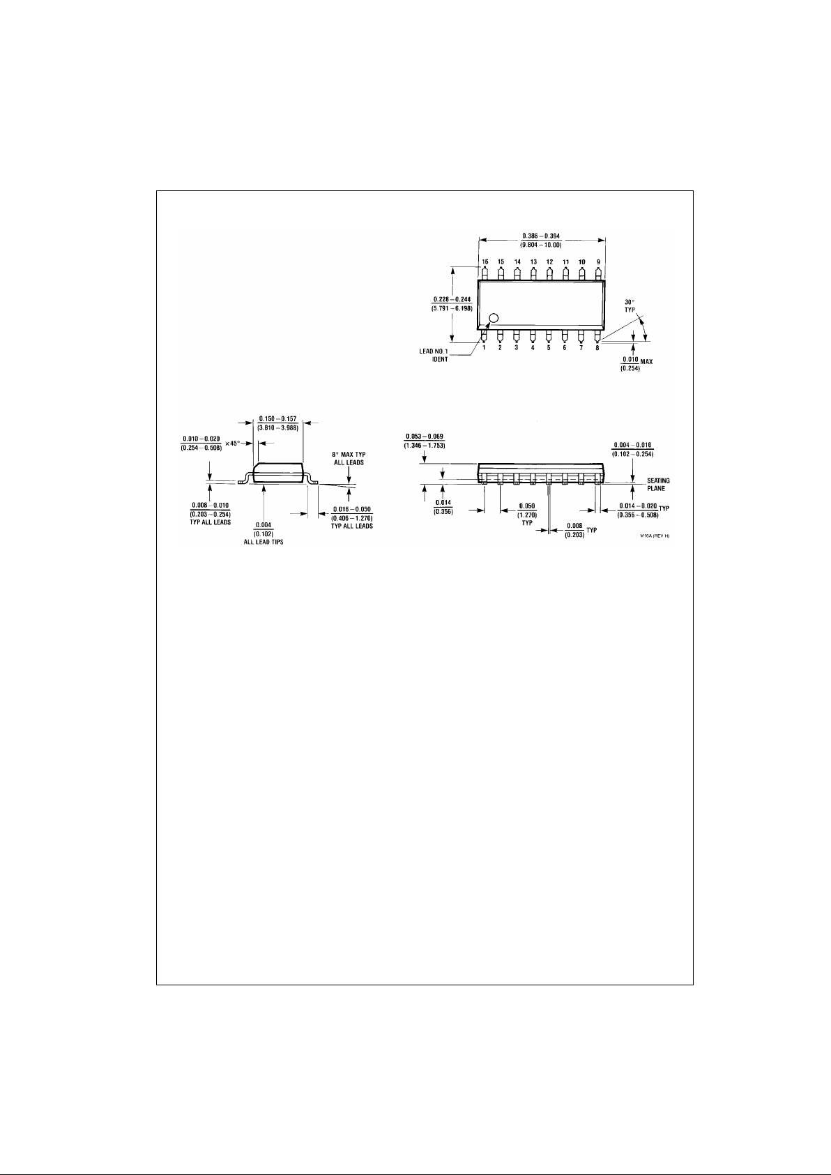
Physical Dimensions inches (millimeters) unless otherwise noted
16-Lead Small Outline Integrated Circuit (SOIC), JEDEC MS-012, 0.150 Narrow
Package Number M16A
Page 9

9 www.fairchildsemi.com
CD4528BC Dual Monostable Multivibrator
Physical Dimensions inches (millimeters) unless otherwise noted (Continued)
16-Lead Plastic Dual-In-Line Package (PDIP), JEDEC MS-001, 0.300 Wide
Package Number N16E
Fairchild does not assume any responsibility for use of any circuitry described , no circuit patent licenses are implied and
Fairchild reserves the right at any time without notice to change said circuitry and specifications.
LIFE SUPPORT POLICY
FAIRCHILD’S PRODUCTS ARE NOT AUTHORIZED FOR USE AS CRITICAL COMPONENTS IN LIFE SUPPORT
DEVICES OR SYSTEMS WITHOUT THE EXPRESS WRITTEN APPROVAL OF THE PRESIDENT OF FAIRCHILD
SEMICONDUCTOR CORPORATION. As used herein:
1. Life support devices o r syst ems are devices or systems
which, (a) are intended for surgical implant into the
body, or (b) support or sustain life, and (c) whose failure
to perform when properly used in accordance with
instructions for use provide d in the labe l ing, can be re asonably expected to result in a significant injury to the
user.
2. A critica l compo nent in any componen t o f a life s upp ort
device or system whose failure to perform can be reasonably expected to cause the failure of the l ife support
device or system, or to affect its safety or effectiveness.
www.fairchildsemi.com
 Loading...