

Page 1
CD4518BMS,
CD4520BMS
December 1992
Features
• High Voltage Types (20V Rating)
• CD4518BMS Dual BCD Up Counter
• CD4520BMS Dual Binary Up Counter
• Medium Speed Operation
- 6MHz Typical Clock Frequency at 10V
• Positive or Negative Edge Triggering
• Synchronous Internal Carry Propagation
• 100% Tested for Quiescent Current at 20V
• 5V, 10V and 15V Parametric Ratings
• Maximum Input Current of 1µA at 18V Over Full Pack-
age Temperature Range; 100nA at 18V and +25
• Noise Margin (Over Full Package/Temperature Range)
- 1V at VDD = 5V
- 2V at VDD = 10V
- 2.5V at VDD = 15V
• Standardized Symmetrical Output Characteristics
• Meets All Requirements of JEDEC Tentative Standard
No. 13B, “Standard Specifications for Description of
‘B’ Series CMOS Devices”
CMOS Dual Up Counters
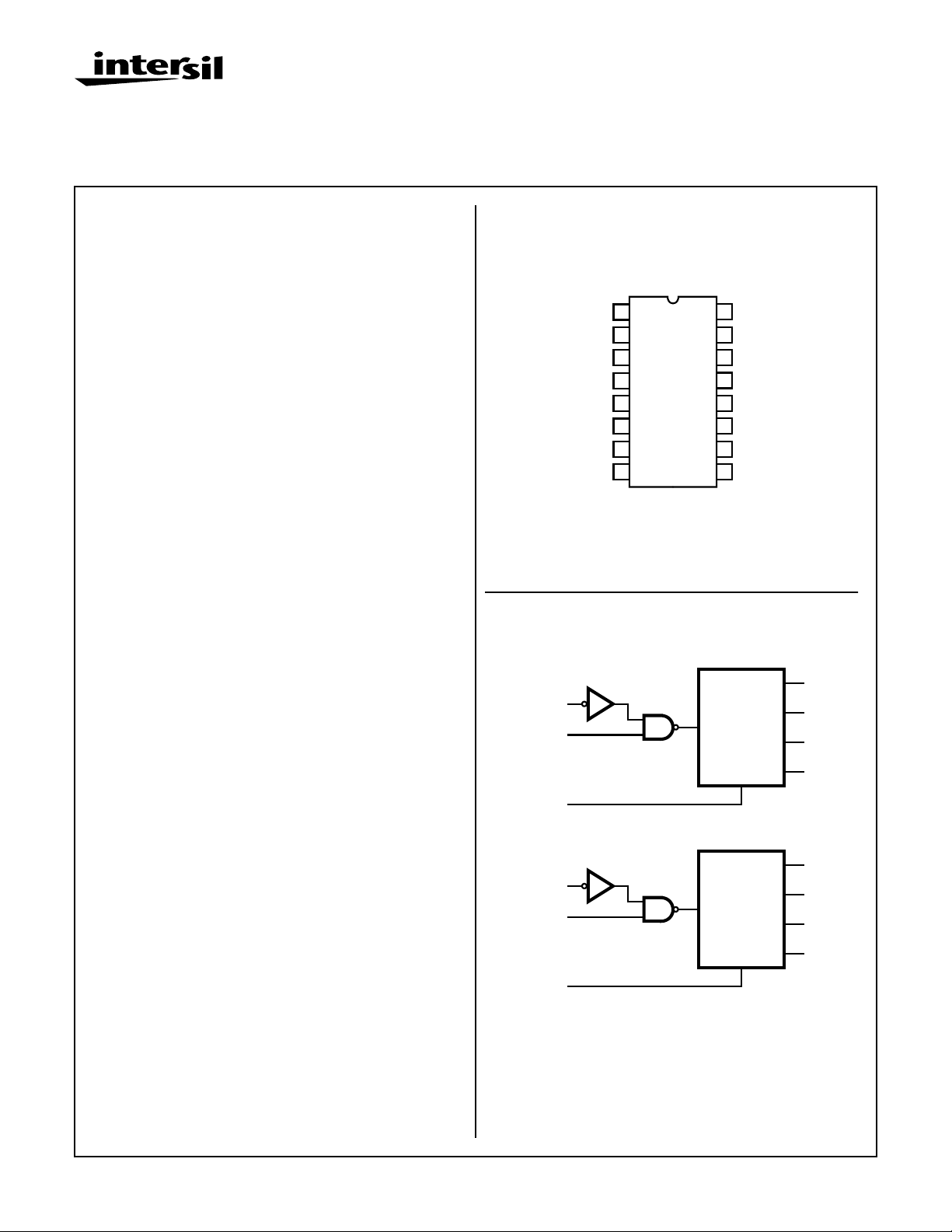
Pinout
CD4518BMS, CD4520BMS
TOP VIEW
VDD
16
15
RESET B
Q4B
14
Q3B
13
Q2B
12
Q1B
11
ENABLE B
10
9
CLOCK B
Q1A
Q2A
Q3A
Q4A
VSS
1
2
3
4
5
6
7
8
CLOCK A
ENABLE A
o
C
RESET A
Functional Diagram
Applications
• Multistage Synchronous Counting
• Multistage Ripple Counting
• Frequency Dividers
Description
CD4518BMS Dual BCD Up Counter and CD4520BMS Dual
Binary Up Counter each consist of two identical, internally
synchronous 4-stage counters. The counter stages are
D-type flip-flops having interchangeable CLOCK and
ENABLE lines for incrementing on either the positive-going
or negative-going transition. For single unit operation the
ENABLE input is maintained high and the counter advances
on each positive-going transition of the CLOCK. The
counters are cleared by high levels on their RESET lines.
The counter can be cascaded in the ripple mode by connecting Q4 to the enable input of the subsequent counter while
the CLOCK input of the latter is held low.
The CD4518BMS and CD4520BMS are supplied in these
16-lead outline packages:
Braze Seal DIP H4S
Frit Seal DIP H1F
Ceramic Flatpack *H6P †H6W
*CD4518B Only †CD4520B Only
CLOCK A
ENABLE A
RESET A
CLOCK B
ENABLE B
10
RESET B
15
3
Q1A
14
2
7
912
÷10/÷16
C
÷10/÷16
C
Q2A
5
Q3A
6
R
R
Q4A
11
Q1B
Q2B
13
Q3B
14
Q4B
VSS = 8
VDD = 16
CAUTION: These devices are sensitive to electrostatic discharge; follow proper IC Handling Procedures.
1-888-INTERSIL or 321-724-7143 | Copyright © Intersil Corporation 1999
7-1206
File Number
3342
Page 2
Specifications CD4518BMS, CD4520BMS
Absolute Maximum Ratings Reliability Information
DC Supply Voltage Range, (VDD) . . . . . . . . . . . . . . . -0.5V to +20V
(Voltage Referenced to VSS Terminals)
Input Voltage Range, All Inputs . . . . . . . . . . . . .-0.5V to VDD +0.5V
DC Input Current, Any One Input . . . . . . . . . . . . . . . . . . . . . . . .±10mA
Operating Temperature Range. . . . . . . . . . . . . . . . -55oC to +125oC
Package Types D, F, K, H
Storage Temperature Range (TSTG) . . . . . . . . . . . -65oC to +150oC
Lead Temperature (During Soldering) . . . . . . . . . . . . . . . . . +265oC
At Distance 1/16 ± 1/32 Inch (1.59mm ± 0.79mm) from case for
10s Maximum
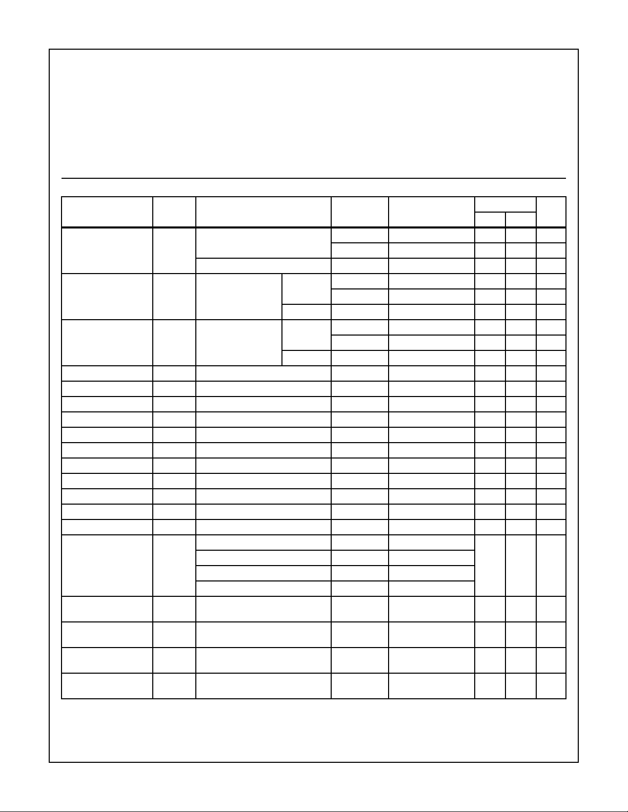
TABLE 1. DC ELECTRICAL PERFORMANCE CHARACTERISTICS
PARAMETER SYMBOL CONDITIONS (NOTE 1)
Supply Current IDD VDD = 20V, VIN = VDD or GND 1 +25oC-10µA
VDD = 18V, VIN = VDD or GND 3 -55oC-10µA
Input Leakage Current IIL VIN = VDD or GND VDD = 20 1 +25oC -100 - nA
VDD = 18V 3 -55oC -100 - nA
Input Leakage Current IIH VIN = VDD or GND VDD = 20 1 +25oC - 100 nA
VDD = 18V 3 -55oC - 100 nA
Output Voltage VOL15 VDD = 15V, No Load 1, 2, 3 +25oC, +125oC, -55oC - 50 mV
Output Voltage VOH15 VDD = 15V, No Load (Note 3) 1, 2, 3 +25oC, +125oC, -55oC 14.95 - V
Output Current (Sink) IOL5 VDD = 5V, VOUT = 0.4V 1 +25oC 0.53 - mA
Output Current (Sink) IOL10 VDD = 10V, VOUT = 0.5V 1 +25oC 1.4 - mA
Output Current (Sink) IOL15 VDD = 15V, VOUT = 1.5V 1 +25oC 3.5 - mA
Output Current (Source) IOH5A VDD = 5V, VOUT = 4.6V 1 +25oC - -0.53 mA
Output Current (Source) IOH5B VDD = 5V, VOUT = 2.5V 1 +25oC - -1.8 mA
Output Current (Source) IOH10 VDD = 10V, VOUT = 9.5V 1 +25oC - -1.4 mA
Output Current (Source) IOH15 VDD = 15V, VOUT = 13.5V 1 +25oC - -3.5 mA
N Threshold Voltage VNTH VDD = 10V, ISS = -10µA 1 +25oC -2.8 -0.7 V
P Threshold Voltage VPTH VSS = 0V, IDD = 10µA 1 +25oC 0.7 2.8 V
Functional F VDD = 2.8V, VIN = VDD or GND 7 +25oC VOH >
VDD = 20V, VIN = VDD or GND 7 +25oC
VDD = 18V, VIN = VDD or GND 8A +125oC
VDD = 3V, VIN = VDD or GND 8B -55oC
Input Voltage Low
(Note 2)
Input Voltage High
(Note 2)
Input Voltage Low
(Note 2)
Input Voltage High
(Note 2)
NOTES: 1. All voltages referenced to device GND, 100% testing being
implemented.
2. Go/No Go test with limits applied to inputs.
VIL VDD = 5V, VOH > 4.5V, VOL < 0.5V 1, 2, 3 +25oC, +125oC, -55oC - 1.5 V
VIH VDD = 5V, VOH > 4.5V, VOL < 0.5V 1, 2, 3 +25oC, +125oC, -55oC 3.5 - V
VIL VDD = 15V, VOH > 13.5V,
VOL < 1.5V
VIH VDD = 15V, VOH > 13.5V,
VOL < 1.5V
Thermal Resistance . . . . . . . . . . . . . . . . θ
Ceramic DIP and FRIT Package. . . . . 80oC/W 20oC/W
Flatpack Package . . . . . . . . . . . . . . . . 70oC/W 20oC/W
Maximum Package Power Dissipation (PD) at +125oC
For TA = -55oC to +100oC (Package Type D, F, K) . . . . . . 500mW
For TA = +100oC to +125oC (Package Type D, F, K). . . . . .Derate
Linearity at 12mW/oC to 200mW
Device Dissipation per Output Transistor . . . . . . . . . . . . . . . 100mW
For TA = Full Package Temperature Range (All Package Types)
Junction Temperature . . . . . . . . . . . . . . . . . . . . . . . . . . . . . . +175oC
GROUP A
SUBGROUPS TEMPERATURE
2 +125oC - 1000 µA
2 +125oC -1000 - nA
2 +125oC - 1000 nA
1, 2, 3 +25oC, +125oC, -55oC- 4 V
1, 2, 3 +25oC, +125oC, -55oC11 - V
3. For accuracy, voltage is measured differentially to VDD. Limit
is 0.050V max.
ja
LIMITS
VDD/2
VOL <
VDD/2
θ
jc
UNITSMIN MAX
V
7-1207
Page 3
Specifications CD4518BMS, CD4520BMS
TABLE 2. AC ELECTRICAL PERFORMANCE CHARACTERISTICS
GROUP A
PARAMETER SYMBOL CONDITIONS (NOTE 1, 2)
Propagation Delay
Clock to Output
Propagation Delay
Reset to Ouput
Transition Time
(Note 2)
Maximum Clock Input
Frequency
NOTES:
1. CL = 50pF, RL = 200K, Input TR, TF < 20ns.
2. -55oC and +125oC limits guaranteed, 100% testing being implemented.
PARAMETER SYMBOL CONDITIONS NOTES TEMPERATURE
Supply Current IDD VDD = 5V, VIN = VDD or GND 1, 2 -55
Output Voltage VOL VDD = 5V, No Load 1, 2 +25oC, +125oC,
Output Voltage VOL VDD = 10V, No Load 1, 2 +25oC, +125oC,
Output Voltage VOH VDD = 5V, No Load 1, 2 +25oC, +125oC,
Output Voltage VOH VDD = 10V, No Load 1, 2 +25oC, +125oC,
Output Current (Sink) IOL5 VDD = 5V, VOUT = 0.4V 1, 2 +125oC 0.36 - mA
Output Current (Sink) IOL10 VDD = 10V, VOUT = 0.5V 1, 2 +125oC 0.9 - mA
Output Current (Sink) IOL15 VDD = 15V, VOUT = 1.5V 1, 2 +125oC 2.4 - mA
Output Current (Source) IOH5A VDD = 5V, VOUT = 4.6V 1, 2 +125oC - -0.36 mA
Output Current (Source) IOH5B VDD = 5V, VOUT = 2.5V 1, 2 +125oC - -1.15 mA
Output Current (Source) IOH10 VDD = 10V, VOUT = 9.5V 1, 2 +125oC - -0.9 mA
Output Current (Source) IOH15 VDD =15V, VOUT = 13.5V 1, 2 +125oC - -2.4 mA
Input Voltage Low VIL VDD = 10V , VOH > 9V, VOL < 1V 1, 2 +25oC, +125oC,
Input Voltage High VIH VDD = 10V, VOH > 9V , VOL < 1V 1, 2 +25oC, +125oC,
TPHL1
TPLH1
TPHL2 VDD = 5V, VIN = VDD or GND 9 +25oC - 650 ns
TTHL
TTLH
FCL VDD = 5V, VIN = VDD or GND 9 +25oC 1.5 - MHz
VDD = 5V, VIN = VDD or GND 9 +25oC - 560 ns
VDD = 5V, VIN = VDD or GND 9 +25oC - 200 ns
TABLE 3. ELECTRICAL PERFORMANCE CHARACTERISTICS
VDD = 10V, VIN = VDD or GND 1, 2 -55oC, +25oC- 10µA
VDD = 15V, VIN = VDD or GND 1, 2 -55oC, +25oC- 10µA
SUBGROUPS TEMPERATURE
10, 11 +125oC, -55oC - 756 ns
10, 11 +125oC, -55oC - 878 ns
10, 11 +125oC, -55oC - 270 ns
10, 11 +125oC, -55oC 1.11 - MHz
o
C, +25oC- 5 µA
+125oC - 150 µA
+125oC - 300 µA
+125oC - 600 µA
-55oC
-55oC
-55oC
-55oC
-55oC 0.64 - mA
-55oC 1.6 - mA
-55oC 4.2 - mA
-55oC - -0.64 mA
-55oC - -2.0 mA
-55oC - -1.6 mA
-55oC - -4.2 mA
-55oC
-55oC
LIMITS
UNITSMIN MAX
LIMITS
UNITSMIN MAX
-50mV
-50mV
4.95 - V
9.95 - V
-3V
+7 - V
7-1208
Page 4

Specifications CD4518BMS, CD4520BMS
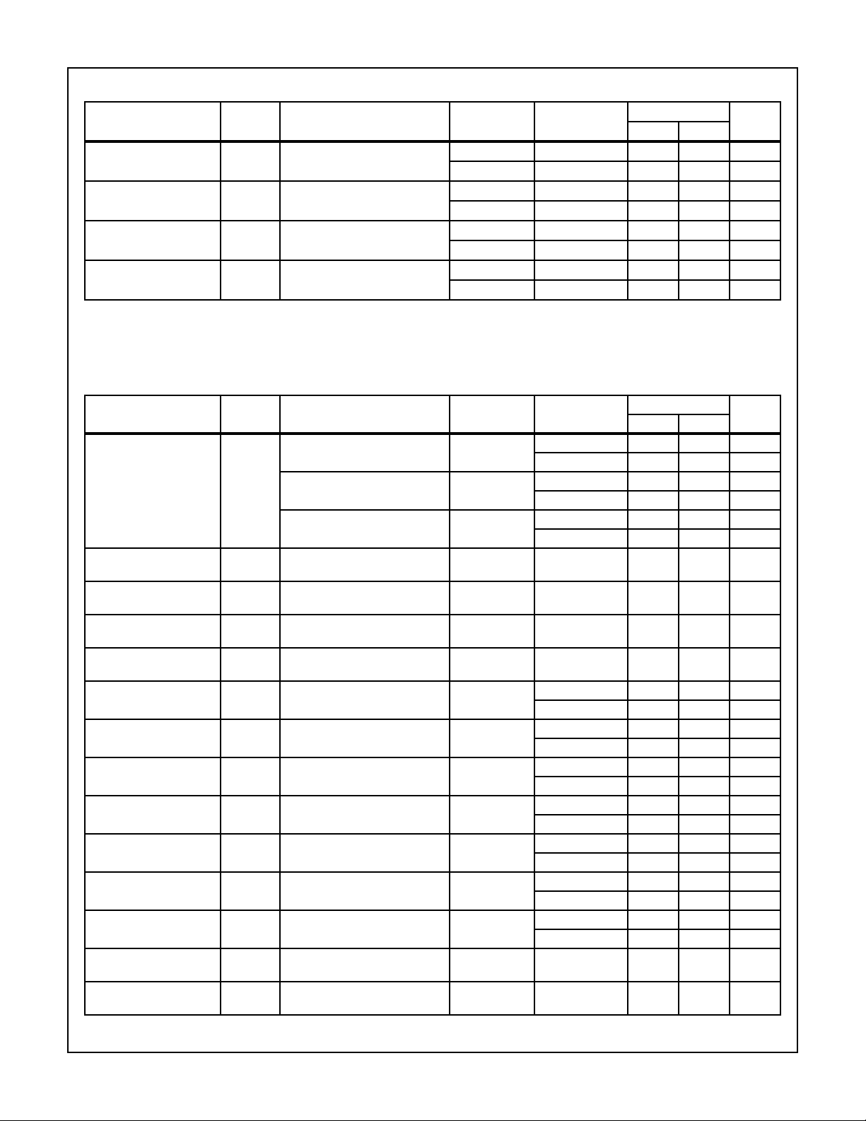
TABLE 3. ELECTRICAL PERFORMANCE CHARACTERISTICS (Continued)
LIMITS
PARAMETER SYMBOL CONDITIONS NOTES TEMPERATURE
Propagation Delay
Clock to Output
Propagation Delay
Reset to Output
Transition Time TTHL
Maximum Clock Input
Frequency
Maximum Clock Rise and
Fall Time
TPHL1
TPLH1
VDD = 10V 1, 2, 3 +25oC - 230 ns
VDD = 15V 1, 2, 3 +25oC - 160 ns
TPHL2 VDD = 10V 1, 2, 3 +25oC - 225 ns
VDD = 15V 1, 2, 3 +25oC - 170 ns
VDD = 10V 1, 2, 3 +25oC - 100 ns
TTLH
VDD = 15V 1, 2, 3 +25oC - 80 ns
FCL VDD = 10V 1, 2, 3 +25oC 3 - MHz
VDD = 15V 1, 2, 3 +25oC 4 - MHz
TRCL
TFCL
VDD = 5V 1, 2, 3, 4 +25oC-15µs
VDD = 10V 1, 2, 3, 4 +25oC-5µs
VDD = 15V 1, 2, 3, 4 +25oC-5µs
Minimum Enable Pulse
Width
TW VDD = 5V 1, 2, 3 +25oC - 400 ns
VDD = 10V 1, 2, 3 +25oC - 200 ns
VDD = 15V 1, 2, 3 +25oC - 140 ns
Minimum Reset Pulse
Width
TW VDD = 5V 1, 2, 3 +25oC - 250 ns
VDD = 10V 1, 2, 3 +25oC - 110 ns
VDD = 15V 1, 2, 3 +25oC - 80 ns
Minimum Clock Pulse
Width
TW VDD = 5V 1, 2, 3 +25oC - 200 ns
VDD = 10V 1, 2, 3 +25oC - 100 ns
VDD = 15V 1, 2, 3 +25oC - 70 ns
Input Capacitance CIN Any Input 1, 2 +25oC - 7.5 pF
NOTES:
1. All voltages referenced to device GND.
2. The parameters listed on Table 3 are controlled via design or process and are not directly tested. These parameters are characterized
on initial design release and upon design changes which would affect these characteristics.
3. CL = 50pF, RL = 200K, Input TR, TF < 20ns.
4. If more than one unit is cascaded, TRCL should be made less than or equal to the sumof the transition time and the fixed propagation
delay of the output of the driving stage for the estimated capacitive load.
UNITSMIN MAX
TABLE 4. POST IRRADIATION ELECTRICAL PERFORMANCE CHARACTERISTICS
PARAMETER SYMBOL CONDITIONS NOTES TEMPERATURE
Supply Current IDD VDD = 20V, VIN = VDD or GND 1, 4 +25
N Threshold Voltage VNTH VDD = 10V, ISS = -10µA 1, 4 +25
N Threshold Voltage
∆VTN VDD = 10V, ISS = -10µA 1, 4 +25
Delta
P Threshold Voltage VTP VSS = 0V, IDD = 10µA 1, 4 +25
P Threshold Voltage
∆VTP VSS = 0V, IDD = 10µA 1, 4 +25
Delta
Functional F VDD = 18V, VIN = VDD or GND 1 +25
VDD = 3V, VIN = VDD or GND
Propagation Delay Time TPHL
VDD = 5V 1, 2, 3, 4 +25oC - 1.35 x
TPLH
NOTES: 1. All voltages referenced to device GND.
2. CL = 50pF, RL = 200K, Input TR, TF < 20ns.
3. See Table 2 for +25
4. Read and Record
7-1209
LIMITS
UNITSMIN MAX
o
C-25µA
o
C -2.8 -0.2 V
o
C-±1V
o
C 0.2 2.8 V
o
C-±1V
o
C VOH >
VDD/2
VOL <
VDD/2
V
ns
+25oC
Limit
o
C limit.
Page 5

Specifications CD4518BMS, CD4520BMS
TABLE 5. BURN-IN AND LIFE TEST DELTA PARAMETERS +25oC
PARAMETER SYMBOL DELTA LIMIT
Supply Current - MSI-2 IDD ± 1.0µA
Output Current (Sink) IOL5 ± 20% x Pre-Test Reading
Output Current (Source) IOH5A ± 20% x Pre-Test Reading
TABLE 6. APPLICABLE SUBGROUPS
MIL-STD-883
CONFORMANCE GROUP
Initial Test (Pre Burn-In) 100% 5004 1, 7, 9 IDD, IOL5, IOH5A
Interim Test 1 (Post Burn-In) 100% 5004 1, 7, 9 IDD, IOL5, IOH5A
Interim Test 2 (Post Burn-In) 100% 5004 1, 7, 9 IDD, IOL5, IOH5A
PDA (Note 1) 100% 5004 1, 7, 9, Deltas
Interim Test 3 (Post Burn-In) 100% 5004 1, 7, 9 IDD, IOL5, IOH5A
PDA (Note 1) 100% 5004 1, 7, 9, Deltas
Final Test 100% 5004 2, 3, 8A, 8B, 10, 11
Group A Sample 5005 1, 2, 3, 7, 8A, 8B, 9, 10, 11
Group B Subgroup B-5 Sample 5005 1, 2, 3, 7, 8A, 8B, 9, 10, 11, Deltas Subgroups 1, 2, 3, 9, 10, 11
Subgroup B-6 Sample 5005 1, 7, 9
Group D Sample 5005 1, 2, 3, 8A, 8B, 9 Subgroups 1, 2 3
NOTE: 1. 5% Parameteric, 3% Functional; Cumulative for Static 1 and 2.
METHOD GROUP A SUBGROUPS READ AND RECORD
TABLE 7. TOTAL DOSE IRRADIATION
MIL-STD-883
CONFORMANCE GROUPS
Group E Subgroup 2 5005 1, 7, 9 Table 4 1, 9 Table 4
FUNCTION OPEN GROUND VDD 9V ± -0.5V
Static Burn-In 1
Note 1
Static Burn-In 2
Note 1
Dynamic BurnIn Note 1
Irradiation
Note 2
NOTES:
1. Each pin except VDD and GND will have a series resistor of 10K ± 5%, VDD = 18V ± 0.5V
2. Each pin except VDD and GND will have a series resistor of 47K ± 5%; Group E, Subgroup 2, sample size is 4 dice/wafer, 0 failures,
VDD = 10V ± 0.5V
3-6, 11-14 1, 2, 7-10, 15 16
3-6, 11-14 8 1, 2, 7, 9, 10,
- 7, 8, 15 2, 10, 16 3-6, 11-14 1, 9
3-6, 11-14 8 1, 2, 7, 9, 10,
METHOD
TABLE 8. BURN-IN AND IRRADIATION TEST CONNECTIONS
PRE-IRRAD POST-IRRAD PRE-IRRAD POST-IRRAD
15, 16
15, 16
TEST READ AND RECORD
OSCILLATOR
50kHz 25kHz
7-1210
Page 6

Logic Diagrams
CD4518BMS, CD4520BMS
ALL INPUTS ARE PROTECTED
*
BY CMOS PROTECTION
NETWORK
*
RESET
7/15
CLOCK
*
2/10
*
1/9
ENABLE
FIGURE 1. DECADE COUNTER (CD4518BMS) LOGIC DIAGRAM FOR ONE OF TWO IDENTICAL COUNTERS
VDD
VDD
VSS
Q1
3/11
QQDC
R
Q1
3/11
Q2
4/12
QQDC
R
Q2
4/12
Q3
5/13
QQDC
R
Q3
5/13
Q4
6/14
QQDC
R
Q4
6/14
ALL INPUTS ARE PROTECTED
*
BY CMOS PROTECTION
NETWORK
*
RESET
7/15
CLOCK
*
2/10
*
1/9
ENABLE
FIGURE 2. BINARY COUNTER (CD4520BMS) LOGIC DIAGRAM FOR ONE OF TWO IDENTICAL COUNTERS
VSS
QQDC
R
QQDC
R
TRUTH TABLE
CLOCK ENABLE RESET ACTION
1 0 Increment Counter
0 0 Increment Counter
X 0 No Change
X 0 No Change
0 0 No Change
1 0 No Change
X X 1 Q1 thru Q4 = 0
X = Don’t Care 1 ≡ High State 0 ≡ Low State
QQDC
R
QQDC
R
7-1211
Page 7

Typical Performance Curves
CD4518BMS, CD4520BMS
AMBIENT TEMPERATURE (TA) = +25oC
30
25
20
15
10
5
OUTPUT LOW (SINK) CURRENT (IOL) (mA)
0 5 10 15
GATE-TO-SOURCE VOLTAGE (VGS) = 15V
10V
5V
DRAIN-TO-SOURCE VOLTAGE (VDS) (V)
FIGURE 3. TYPICAL OUTPUT LOW (SINK) CURRENT
CHARACTERISTICS
DRAIN-TO-SOURCE VOLTAGE (VDS) (V)
AMBIENT TEMPERATURE (TA) = +25oC
GATE-TO-SOURCE VOLTAGE (VGS) = -5V
-10V
AMBIENT TEMPERATURE (TA) = +25oC
15.0
12.5
10.0
7.5
5.0
2.5
OUTPUT LOW (SINK) CURRENT (IOL) (mA)
0 5 10 15
GATE-TO-SOURCE VOLTAGE (VGS) = 15V
10V
5V
DRAIN-TO-SOURCE VOLTAGE (VDS) (V)
FIGURE 4. MINIMUM OUTPUT LOW (SINK) CURRENT
CHARACTERISTICS
0-5-10-15
0
-5
-10
-15
-20
DRAIN-TO-SOURCE VOLTAGE (VDS) (V)
AMBIENT TEMPERATURE (TA) = +25oC
GATE-TO-SOURCE VOLTAGE (VGS) = -5V
-10V
0-5-10-15
0
-5
-10
-25
-15V
-30
FIGURE 5. TYPICAL OUTPUT HIGH (SOURCE) CURRENT
CHARACTERISTICS
350
AMBIENT TEMPERATURE (TA) = +25oC
300
250
200
150
100
50
PROPAGATION DELAY TIME (tPLH, tPHL) (ns)
0
10
20 30 40 50 60 70 80 90 100
LOAD CAPACITANCE (CL) (pF)
SUPPLY VOLTAGE (VDD) = 5V
10V
15V
-15V
OUTPUT HIGH (SOURCE) CURRENT (IOH) (mA)
FIGURE 6. MINIMUM OUTPUT HIGH (SOURCE) CURRENT
CHARACTERISTICS
350
AMBIENT TEMPERATURE (TA) = +25oC
300
250
200
150
100
50
PROPAGATION DELAY TIME (tPHL, tPLH) (ns)
0
10
20 30 40 50 60 70 80 90 100
SUPPLY VOLTAGE (VDD) = 5V
10V
15V
LOAD CAPACITANCE (CL) (pF)
-15
OUTPUT HIGH (SOURCE) CURRENT (IOH) (mA)
110
FIGURE 7. TYPICAL PROPAGATION DELAY vs LOAD CAPAC-
ITANCE, CLOCK OR ENABLE TO OUTPUT
7-1212
FIGURE 8. TYPICAL PROPAGATION DELAY TIME vs LOAD
CAPACITANCE, RESET TO OUTPUT
Page 8

Typical Performance Curves
CD4518BMS, CD4520BMS
AMBIENT TEMPERATURE (TA) = +25oC
200
150
100
50
TRANSITION TIME (tTHL, tTLH) (ns)
0
0 40 60 80 10020
SUPPLY VOLTAGE (VDD) = 5V
LOAD CAPACITANCE (CL) (pF)
10V
15V
MAXIMUM CLOCK FREQUENCY (fCL MAX) (MHz)
AMBIENT TEMPERATURE (TA) = +25oC
LOAD CAPACITANCE (CL) = 50PF
15
10
5
0 5 10 15 20
SUPPLY VOLTAGE (VDD) (V)
FIGURE 9. TYPICAL TRANSITION TIME vs LOAD CAPACITANCE FIGURE 10. TYPICAL MAXIMUM CLOCK FREQUENCY vs
SUPPLY VOLTAGE
4
10
8
6
SUPPLY VOLTAGE (VDD) = 15V
4
2
3
10
8
6
4
2
10
10
POWER DISSIPATION /CONVERTER (PD) (µW)
2
8
6
4
2
8
6
4
2
1
0.1 1
5V
CL = 50pF
CL = 15pF
AMBIENT TEMPERATURE (TA) = +25oC
8642
8642
10
FREQUENCY (f) (kHz)
8642
2
10
10V
8642
10V
8642
3
10
4
10
FIGURE 11. TYPICAL POWER DISSIPATION CHARACTERISTICS
Timing Diagrams
CD4518BMS
CD4520BMS
123456789
10 11 12 13 14 15 16 17 18
CLOCK
ENABLE
RESET
123456789 1234567890
0
Q1
Q2
Q3
Q4
12345678910111213141501234
Q1
Q2
Q3
Q4
FIGURE 12. TIMING DIAGRAMS FOR CD4518BMS AND CD4520BMS
7-1213
Page 9

CLOCK
INPUT
VDD
2
CD4518BMS, CD4520BMS
71
10
159
2
71
10
159
CLOCK
ENABLE
A
Q1A Q2A Q3A Q4A
456
3
RESET
A
FIGURE 13. RIPPLE CASCADING OF FOUR COUNTERS WITH POSITIVE EDGE TRIGGERING
CLOCK*
INPUT
2
CLOCK
ENABLE
A
Q1A Q2A Q3A Q4A
456
3
RESET
A
CD4520BMS
CLOCK
A
CD4518BMS/20BMS CD4518BMS/20BMS
31
A
ENABLE
B
Q1B Q2B Q3B Q4B
12 13 14
11
10
CLOCK
ENABLE
B
Q1B Q2B Q3B Q4B
12 13 14
11
RESET
B
B
B
159
RESET
B
CD4071
CLOCK
ENABLE
A
Q1A Q2A Q3A Q4A
456
3
CLOCK
ENABLE
A
Q1A Q2A Q3A Q4A
456
3
A
2
A
RESET
A
31
RESET
A
CD4520BMS
CLOCK
B
Q1B Q2B Q3B Q4B
11
CD4071
CLOCK
B
Q1B Q2B Q3B Q4B
11
ENABLE
12 13 14
10
ENABLE
12 13 14
RESET
B
159
RESET
B
B
B
CD4012A
CD4012ACD4012A
CD4520BMS
* For synchronous cascading, the clock transition time should be made less than or equal to the sum of the fixed propagation delay at 15pF
and the transition time of the output driver stage for the estimated capacitive load.
FIGURE 14. SYNCHRONOUS CASCADING OF FOUR BINARY COUNTERS WITH NEGATIVE EDGE TRIGGERING
7-1214
Page 10

CD4518BMS, CD4520BMS
Chip Dimensions and Pad Layouts
CD4518BMS CD4520BMS
Dimensions in parenthesis are in millimeters and are
derived from the basic inch dimensions as indicated.
Grid graduations are in mils (10-3 inch).
METALLIZATION: Thickness: 11kÅ− 14kÅ, AL.
PASSIVATION: 10.4kÅ - 15.6kÅ, Silane
BOND PADS: 0.004 inches X 0.004 inches MIN
DIE THICKNESS: 0.0198 inches - 0.0218 inches
All Intersil semiconductor products are manufactured, assembled and tested under ISO9000 quality systems certification.
Intersil products are sold by description only. Intersil Corporation reserves the right to make changes in circuit design and/or specifications at any time without
notice. Accordingly, the reader is cautioned to verify that data sheets are current before placing orders. Information furnished by Intersil is believed to be accurate
and reliable. However, no responsibility is assumed by Intersil or its subsidiaries for its use; nor for any infringements of patents or other rights of third parties which
may result from its use. No license is granted by implication or otherwise under any patent or patent rights of Intersil or its subsidiaries.
For information regarding Intersil Corporation and its products, see web site http://www.intersil.com
Sales Office Headquarters
NORTH AMERICA
Intersil Corporation
P. O. Box 883, Mail Stop 53-204
Melbourne, FL 32902
TEL: (321) 724-7000
FAX: (321) 724-7240
EUROPE
Intersil SA
Mercure Center
100, Rue de la Fusee
1130 Brussels, Belgium
TEL: (32) 2.724.2111
FAX: (32) 2.724.22.05
ASIA
Intersil (Taiwan) Ltd.
Taiwan Limited
7F-6, No. 101 Fu Hsing North Road
Taipei, Taiwan
Republic of China
TEL: (886) 2 2716 9310
FAX: (886) 2 2715 3029
1215
 Loading...