Page 1

© 2000 Fairchild Semiconductor Corporation DS005994 www.fairchildsemi.com
October 1987
Revised August 2000
CD4514BC• CD4515BC 4-Bit Latched/4-to-16 Line Decoders
CD4514BC• CD4515BC
4-Bit Latched/4-to-16 Line Decoders
General Description
The CD4514BC and CD45 15BC are 4 -to-16 lin e decoders
with latched inputs implemented with complementary MOS
(CMOS) circuits constructed with N- and P-channel
enhancement mode transistor s. These circuits are primarily used in decoding applications where low power dissipation and/or high noise immunity is required.
The CD4514BC (output a cti ve h igh op ti on ) pr ese nts a lo gi cal “1” at the selected output, whereas the CD4515BC presents a logical “0” at the selected output. Th e in put latches
are R–S type flip-flops, which hold the last input data presented prior to the strobe transition from “1” to “0”. This
input data is decoded and the corresponding output is ac tivated. An output inhibit line is also available.
Features
■ Wide supply voltage range: 3.0V to 15V
■ High noise immunity: 0.45 V
DD
(typ.)
■ Low power TTL: fan out of 2
compatibility: driving 74L
■ Low quiesc ent power dissipation:
0.025
µW/package @ 5.0 V
DC
■ Single supply operation
■ Input impedance
= 1012Ω typically
■ Plug-in replacement for MC14514, MC14515
Ordering Code:
Devices also available in Tape and Reel. Specify by appending suffix letter “X” to the ordering co de.
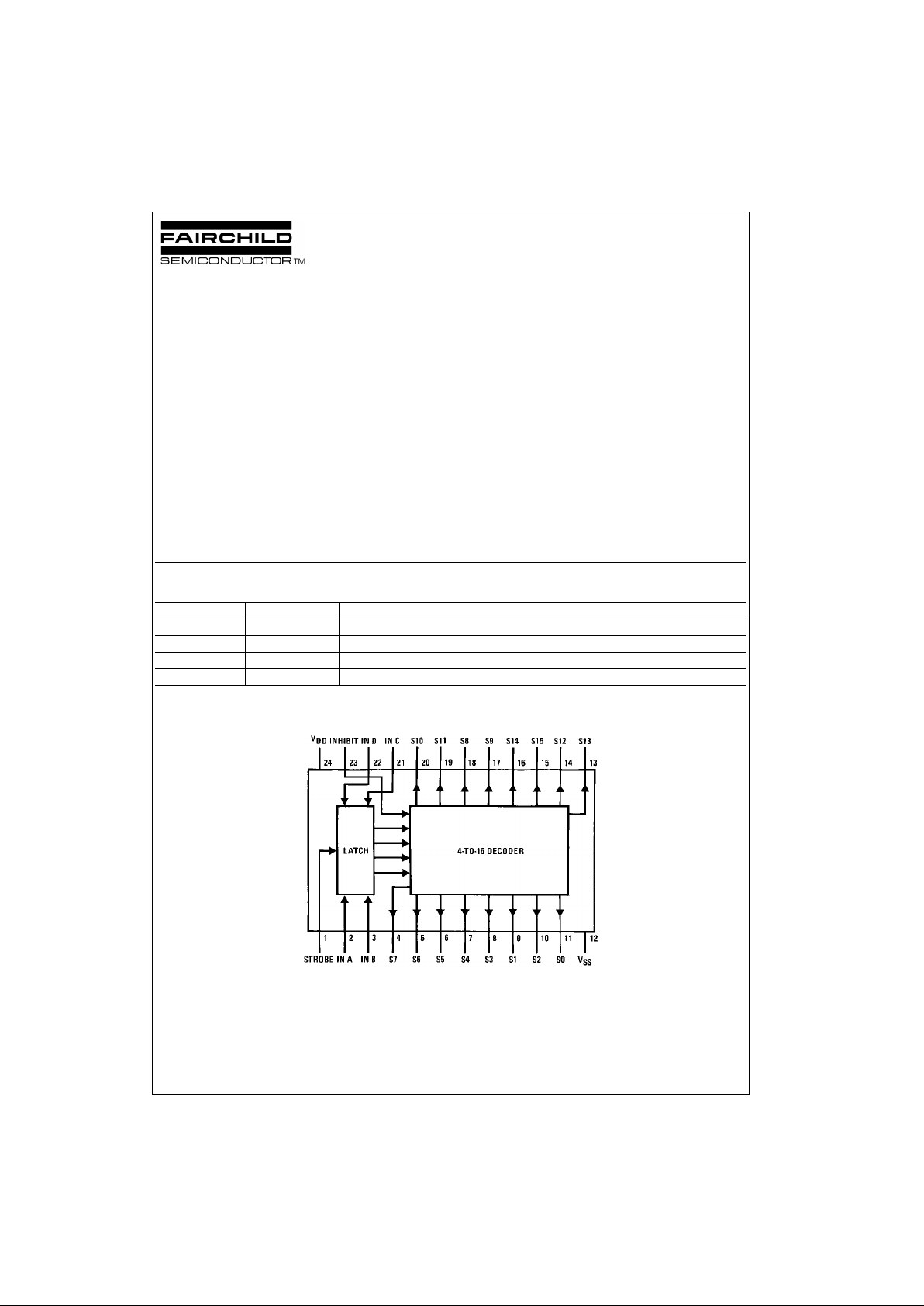
Connection Diagram
Top View
Order Number Package Number Package Diagram
CD4514BCWM M24B 24-Lead Small Outline Integrated Circuit (SOIC), JEDEC MS-013, 0.300 Wide
CD4514BCN N24A 24-Lead Pla sti c Dual-In-Line Package (PDIP), JEDEC MS-0 11, 0.600 Wide
CD4515BCWM M24B 24-Lead Small Outline Integrated Circuit (SOIC), JEDEC MS-013, 0.300 Wide
CD4515BCN N24A 24-Lead Pla sti c Dual-In-Line Package (PDIP), JEDEC MS-0 11, 0.600 Wide
Page 2

www.fairchildsemi.com 2
CD4514BC• CD4515BC
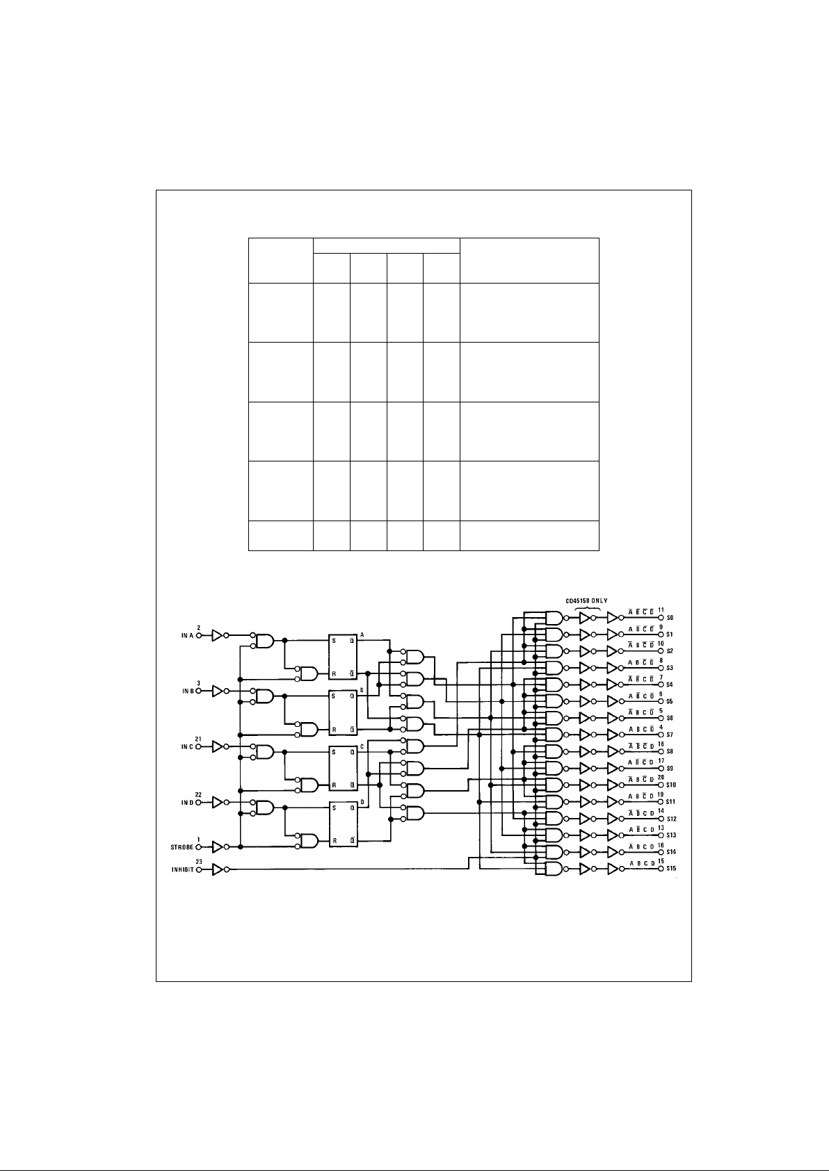
Truth Table
Decode Truth Table (Strobe = 1)
X = Don’t Care
Logic Diagram
Data Inputs Selected Output
Inhibit D C B A CD4514
= Logic “1”
CD4515
= Logic “0”
0 0 0 0 0 S0
0 0 0 0 1 S1
0 0 0 1 0 S2
0 0 0 1 1 S3
0 0 1 0 0 S4
0 0 1 0 1 S5
0 0 1 1 0 S6
0 0 1 1 1 S7
0 1 0 0 0 S8
0 1 0 0 1 S9
0 1 0 1 0 S10
0 1 0 1 1 S11
0 1 1 0 0 S12
0 1 1 0 1 S13
0 1 1 1 0 S14
0 1 1 1 1 S15
1 X X X X All Outputs
= 0, CD4514
All Outputs
= 1, CD4515
Page 3

3 www.fairchildsemi.com
CD4514BC• CD4515BC
Absolute Maximum Ratings(Note 1)
(Note 2)
Recommended Operating
Conditions
(Note 2)
Note 1: “Absolute Maximum Ratings” are those values bey ond which the
safety of the device cannot be guaranteed. Except for “Operating Temperature Range” they are not meant to imply that the devic es should be operated at these limit s. The tables of “Recommended O perating Condit ions”
and “Electrical Characteristics” provide conditions for actual device opera-
tion.
Note 2: V
SS
= 0V unless otherw is e s pecified.
DC Electrical Characteristics (Note 2)
CD4514BC, CD4515BC
Note 3: IOH and IOL are tested one output at a ti m e.
DC Supply Voltage (VDD) −0.5V to +18V
Input Voltage (V
IN
) −0.5V to VDD + 0.5V
Storage Temperature Range (T
S
) −65°C to +150°C
Power Dissipation (P
D
)
Dual-In-Line 700 mW
Small Outline 500 mW
Lead Temperature (T
L
)
(Soldering, 10 seconds) 260
°C
DC Supply Voltage (V
DD
) 3V to 15V
Input Voltage (V
IN
) 0V to V
DD
Operating Temperature Range (TA)
CD4514BC, CD4515BC
−40°C to +85°C
Symbol Parameter Conditions
−40°C +25°C +85°C
Units
Min Max Min Typ Max Min Max
I
DD
Quiescent Device VDD = 5V, VIN = VDD or V
SS
20 0.005 20 150 µA
Current VDD = 10V, VIN = VDD or V
SS
40 0.010 40 300 µA
V
DD
= 15V, VIN = VDD or V
SS
80 0.015 80 600 µA
V
OL
LOW Level VIL = 0V, VIH = VDD,
Output Voltage |IO| < 1 µA
V
DD
= 5V 0.05 0 0.05 0.05 V
V
DD
= 10V 0.05 0 0.05 0.05 V
VDD = 15V 0.05 0 0.05 0.05 V
V
OH
HIGH Level VIL = 0V, VIH = VDD,
Output Voltage |I
O
| < 1 µA
VDD = 5V 4.95 4.95 5.0 4.95 V
V
DD
= 10V 9.95 9.95 10.0 9.95 V
V
DD
= 15V 14.95 14.95 15.0 14.95 V
V
IL
LOW Level |IO| < 1 µA
Input Voltage V
DD
= 5V, VO = 0.5V or 4.5V 1.5 2.25 1.5 1.5 V
V
DD
= 10V, VO = 1.0V or 9.0V 3.0 4.50 3.0 3.0 V
VDD = 15V, VO = 1.5V or 13.5V 4.0 6.75 4.0 4.0 V
V
IH
HIGH Level |IO| < 1 µA
Input Voltage V
DD
= 5V, VO = 0.5V or 4.5V 3.5 3.5 2.75 3.5 V
VDD = 10V, VO = 1.0V or 9.0V 7.0 7.0 5.50 7.0 V
V
DD
= 15V, VO = 1.5V or 13.5V 11.0 11.0 8.25 11.0 V
I
OL
LOW Level Output VDD = 5V, VO = 0.4V 0.52 0.44 0.88 0.36 mA
Current (Note 3) VDD = 10V, VO = 0.5V 1.3 1.1 2.25 0.90 mA
VDD = 15V, VO = 1.5V 3.6 3.0 8.8 2.4 mA
I
OH
HIGH Level Output VDD = 5V, VO = 4.6V −0.52 −0.44 −0.88 −0.36 mA
Current (Note 3) VDD = 10V, VO = 9.5V −1.3 −1.1 −2.25 −0.90 mA
VDD = 15V, VO = 13.5V −3.6 −3.0 −8.8 −2.4 mA
I
IN
Input Current VDD = 15V, VIN = 0V −0.3 −10−5 −0.3 −1.0 µA
VDD = 15V, VIN = 15V 0.3 10−5 0.3 1.0 µA
Page 4

www.fairchildsemi.com 4
CD4514BC• CD4515BC
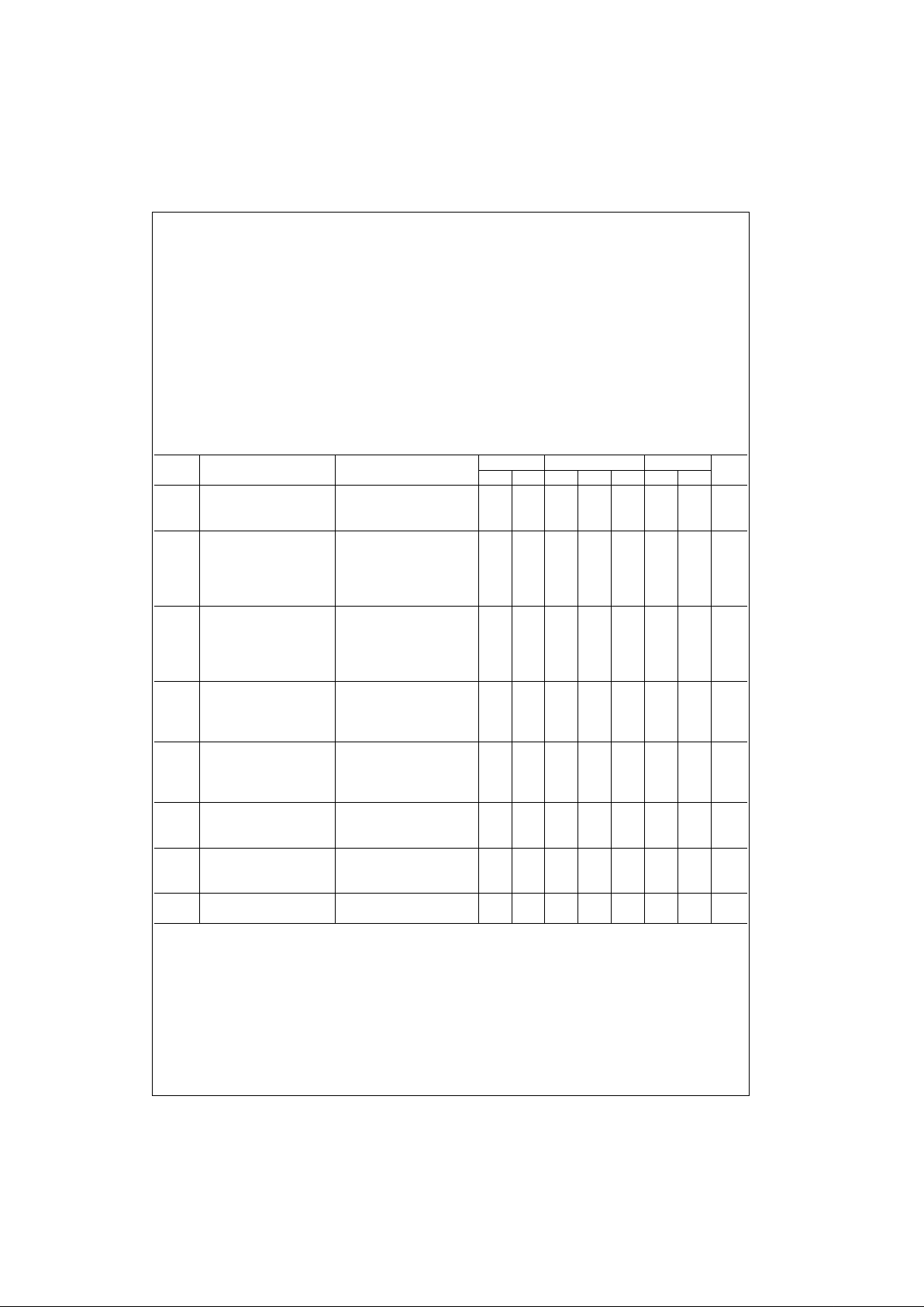
AC Electrical Characteristics (Note 4)
All types C
L
= 50 pF, TA = 25°C, tr = t
f
= 20 ns unless otherwise specified
Note 4: AC Parameters are gu aranteed by DC correlat ed testing.
Note 5: C
PD
determines the no load AC power consumption of any CMOS device. For complete explanation, see Family Characteristics application note,
AN-90.
Note 6: Capacitance is guaranteed by periodic testi ng.
Symbol Parameter Conditions Min Typ Max Units
t
THL
, t
TLH
Transition Times VDD = 5V 100 200 ns
VDD = 10V 50 100 ns
V
DD
= 15V 40 80 ns
t
PLH
, t
PHL
Propagation Delay Times VDD = 5V 550 1100 ns
VDD = 10V 225 450 ns
V
DD
= 15V 150 300 ns
t
PLH
, t
PHL
Inhibit Propagation VDD = 5V 400 800 ns
Delay Times VDD = 10V 150 300 ns
V
DD
= 15V 100 200 ns
t
SU
Setup Time VDD = 5V 125 250 ns
VDD = 10V 50 100 ns
V
DD
= 15V 38 75 ns
t
WH
Strobe Pulse Width VDD = 5V 175 350 ns
VDD = 10V 50 100 ns
VDD = 15V 38 75 ns
C
PD
Power Dissipation Capacitance Per Package (Note 5) 150 pF
C
IN
Input Capacitance Any Input (Note 6) 5 7.5 pF
Page 5

5 www.fairchildsemi.com
CD4514BC• CD4515BC
AC Test Circuit and Switching Time Waveforms
FIGURE 1.
Page 6

www.fairchildsemi.com 6
CD4514BC• CD4515BC
Applications
Two CD4512 8-channel data selectors are used her e with
the CD4514B 4-bit lat ch/decoder to effect a co mplex data
routing system. A total o f 16 in puts fr om da ta regis ters are
selected and transf erred via a 3- STATE data bus to a data
distribut or f o r r e ar ra n gem en t an d en try i n to 16 o ut p ut r e gi sters. In this way sequ ential data can be re-routed o r intermixed according to patte rn s dete rm ined by da ta se lect an d
distribution inputs.
Data is placed into the routing scheme via the 8 inpu ts on
both CD4512 data select ors. One register is assigned to
each input. The signals on A0, A1 and A2 choose 1-of-8
inputs for transfe r out to the 3-STATE data bus. A fourth
signal, labelled D is, disabl es one of the CD 4512 sel ector s,
assuring transfer of data from only one register.
In addition to a choice of input regist ers, 1–16, the rate of
transfer of the sequential information c an also be varied.
That is, if the CD4 512 were addressed at a rate that is 8
times faster than the shift fre quency of the inp ut registers,
the most significant bit (MSB) fr om each reg ister could be
selected for transfer to the data bus. Th erefore, all of the
most significant bits from all of the registers can be transferred to the data bus before the next mo st sign ifican t bit is
presented for transfer by the input registers.
Information from the 3- STATE bus is redistributed by the
CD4514B 4-bit latch/decoder. Using the 4-bit address,
INA–IND, the information on the inhibit line can be transferred to the addres sed output line to the desi red output
registers, A–P. This distribution of data bits to the output
registers can be made in many complex patterns. For
example, all of the most significant bits from the input registers can be routed into output register A, all of the next
most significant bits into register B, etc. In this way horizontal, vertical, or other methods of d ata slicing c an be imp lemented.
Page 7

7 www.fairchildsemi.com
CD4514BC• CD4515BC
Physical Dimensions inches (millimeters) unless otherwise noted
24-Lead Small Outline Integrated Circuit (SOIC), JEDEC MS-013, 0.300 Wide
Package Number M24B
Page 8

www.fairchildsemi.com 8
CD4514BC• CD4515BC 4-Bit Latched/4-to-16 Line Decoders
Physical Dimensions inches (millimeters) unless otherwise noted (Continued)
24-Lead Plastic Dual-In-Line Package (PDIP), JEDEC MS-011, 0.600 Wide
Package Number N24A
Fairchild does not assume any responsibility for use of any circuitr y described, no circuit patent licenses are implied and
Fairchild reserves the right at any time without notice to change said circuitry and specifications.
LIFE SUPPORT POLICY
FAIRCHILD’S PRODUCTS ARE NOT AUTHORIZED FOR USE AS CRITICAL COMPONENTS IN LIFE SUPPORT
DEVICES OR SYSTEMS WITHOUT THE EXPRESS WRITTEN APPROVAL OF THE PRESIDENT OF FAIRCHILD
SEMICONDUCTOR CORPORATION. As used herein:
1. Life support devices or systems are devices or syste ms
which, (a) are intended for surgical implant into the
body, or (b) support or sustain life, and (c) whose failure
to perform when properly used in accordance with
instructions for use provided in the labeling, can be reasonably expected to result in a significant inju ry to the
user.
2. A critical component in any compon ent of a lif e supp ort
device or system whose failure t o perform can be reasonably expected to ca use the failure of the life supp ort
device or system, or to affect its safety or effectiveness.
www.fairchildsemi.com
 Loading...