

Page 1
October 1987
Revised January 1999
CD4512BC 8-Channel Buffered Data Selector
© 1999 Fairchild Semiconductor Corporation DS005993.prf www.fairchildsemi.com
CD4512BC
8-Channel Buffered Data Selector
General Description
The CD4512BC buffered 8-channel da ta se lecto r is a com plementary MOS (CMOS) circuit constructed with N- and
P-channel enhancement mode transistors. This data selec tor is primarily used as a digital signal multiplexer selecting
1 of 8 inputs and routing the signal to a 3-STATE output. A
high level at the Inhibit input forces a low level at the output. A high level at the Output Enable
(OE) input forces the
output into the 3-STATE condition. Low levels at both the
Inhibit and (OE
) inputs allow normal operation.
Features
■ Wide supply voltage range: 3.0V to 15V
■ High noise immunity: 0.45 V
DD
(typ.)
■ 3-STATE output
■ Low quiescent power dissipation:
0.25 µW/package (typ.) @ V
CC
= 5.0V
■ Plug-in replacement for Motorola MC14512
Ordering Code:
Devices also available in Tape and Reel. Specify by appending suffix “X” to the order ing code.
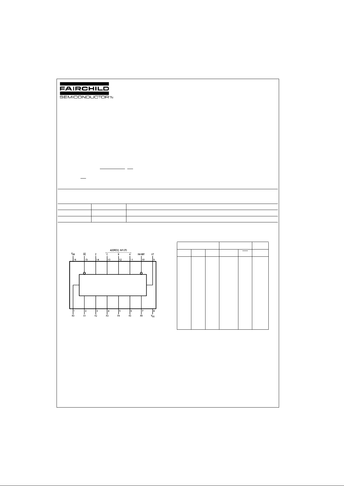
Connection Diagram
Pin Assignments for SOIC an d DIP
Top View
Truth Table
2 = Don't care
Hi-Z = 3-STATE condition
Xn = Data at input n
Order Number Package Number Package Description
CD4512BCM M16A 16-Lead Small Outline Integrated Circuit (SOIC), JEDEC MS-012, 0.150” Narrow Body
CD4512BCN N16E 16-Lead Plastic Dual-In-Line Package (PDIP), JEDEC MS-001, 0.300” Wide
Address Inputs Control Inputs Output
C B A Inhibit OE
Z
000 0 0 X0
001 0 0X1
0 10 0 0X2
011 0 0X3
100 0 0 X4
101 0 0X5
1 10 0 0X6
111 0 0X7
211 1 0 0
2 2 2 2 1 Hi-Z
Page 2
www.fairchildsemi.com 2
CD4512BC
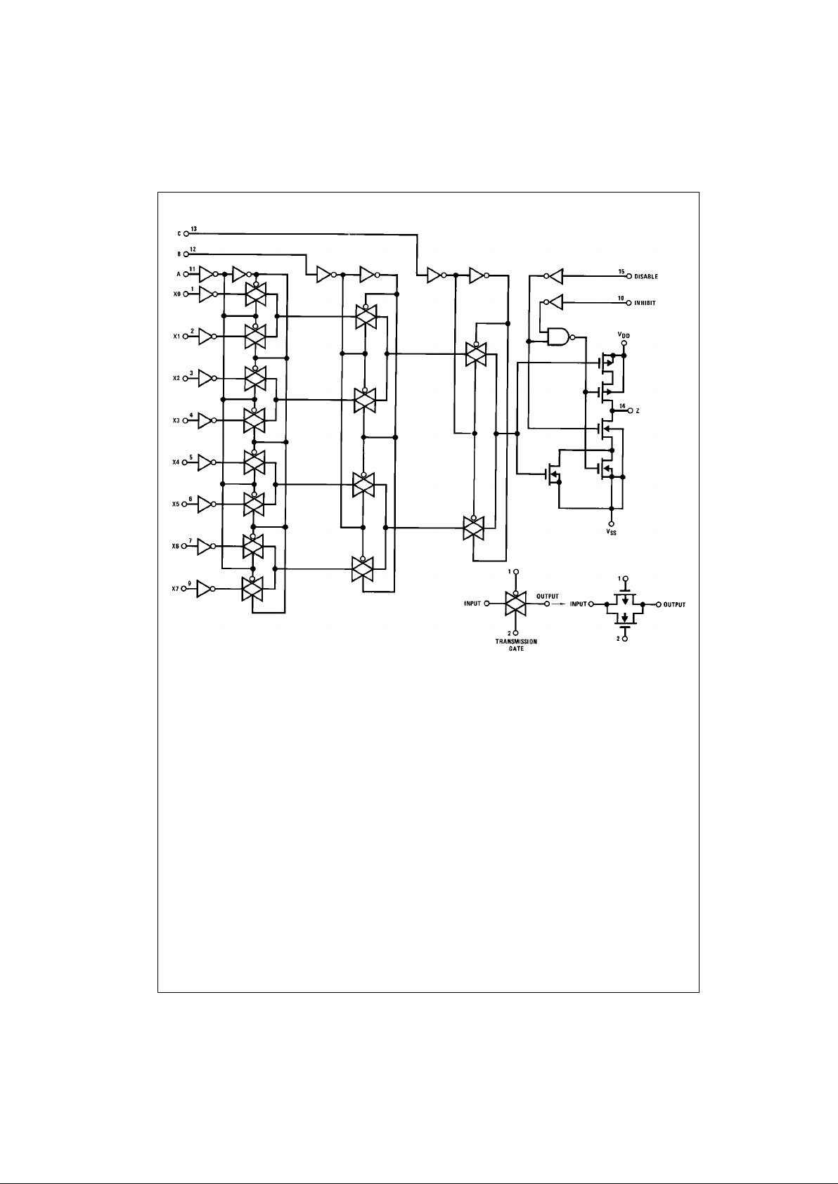
Logic Diagram
Page 3
3 www.fairchildsemi.com
CD4512BC
Absolute Maximum Ratings(Note 1)
(Note 2)
Recommended Operating
Conditions
(Note 2)
Note 1: “Absolute Maximum Rat ings” are tho se values beyond which the
safety of the device cannot be guaranteed. They are not meant to imply
that the devices shoul d be operated at these limits. The Recommend ed
Operating Conditio ns and Electrical Characteris tics table provide conditions for actual device operatio n.
Note 2: V
SS
= 0V unless otherw is e s pecified.
DC Electrical Characteristics (Note 2)
Note 3: IOH and IOL are tested one output at a ti m e.
Supply Voltage (VDD) −0.5 to +18 V
DC
Input Voltage (VIN) −0.5 to VDD + 0.5 V
DC
Storage Temperatur e Range (TS) −65°C to +150°C
Power Dissipa tion (P
D
)
Dual-In-Line 700 mW
Small Outline 500 mW
Lead Temperature, (T
L
)
(Soldering, 10 seconds) 260°C
DC Supply Voltage (V
DD
) 3.0 to 15 V
DC
Input Voltage (VIN) 0 to VDD V
DC
Operating Temperature Range (TA) −40°C to +85°C
Symbol Parameter Conditions
−40°C +25°C +85°C
Units
Min Max Min Typ Max Min Max
I
DD
Quiescent Device VDD = 5V, VIN = VDD or V
SS
20 0.005 20 150 µA
Current VDD = 10V, VIN = VDD or V
SS
40 0.010 40 300 µA
VDD = 15V, VIN = VDD or V
SS
80 0.015 80 600 µA
V
OL
LOW Level VDD = 5V 0.05 0 0.05 0.05 V
Output Voltage VDD = 10V |IOL| < 1 µA 0.05 0 0.05 0.05 V
VDD = 15V 0.05 0 0.05 0.05 V
V
OH
HIGH Level VDD = 5V 4.95 4.95 5.0 4.95 V
Output Voltage VDD = 10V |I
OH
| < 1 µA 9.95 9.95 10.0 9.95 V
VDD = 15V 14.95 14.95 15.0 14.95 V
V
IL
LOW Level VDD = 5V, VO = 0.5V 1.5 2.25 1.5 1.5 V
Input Voltage VDD = 10V, VO = 1.0V 3.0 4.50 3.0 3.0 V
VDD = 15V, VO = 1.5V 4.0 6.75 4.0 4.0 V
V
IH
HIGH Level VDD = 5V, VO = 4.5V 3.5 3.5 2.75 3.5 V
Input Voltage VDD = 10V, VO = 9.0V 7.0 7.0 5.50 7.0 V
VDD = 15V, VO = 13.5V 11.0 11.0 8.25 11.0 V
I
OL
LOW Level Output VDD = 5V, VO = 0.4V 0.52 0.44 0.78 0.36 mA
Current VDD = 10V, VO = 0.5V 1.3 1.1 2.0 0.9 mA
(Note 3) VDD = 15V, VO = 1.5V 3.6 3.4 7.8 2.4 mA
I
OH
HIGH Level Output VDD = 5V, VO = 4.6V −0.2 −0.16 −0.12 mA
Current VDD = 10V, VO = 9.5 −0.5 −0.4 −0.3 mA
(Note 3) VDD = 15V, V O = 13.5V −1.4 −1.2 −1.0 mA
I
IN
Input Current VDD = 15V, VIN = 0V −0.3 −10−5−0.3 −1.0 µA
VDD = 15V, VIN = 15V 0.3 10−50.3 1.0 µA
I
OZ
3-STATE VDD = 15V, VO = 0V ±1.0 ±10
−5
±1.0 ±7.5 µA
Output Current VDD = 15V, VO = 15V
Page 4

www.fairchildsemi.com 4
CD4512BC
AC Electrical Charac teristics (Note 4)
T
A
= 25°C, tr = tf = 20 ns, CL = 50 pF
Note 4: AC Parameters are guara nt eed by DC correlated testin g.
Note 5: Capacitance guaranteed by periodic testing.
Note 6: C
PD
determines the no load AC power of any CMOS device. For comple te expla nation, see Family Characteris t ic s A pplication Note, AN-90.
Symbol Parameter Conditions
CD4512BM CD4512BC
Units
Min Typ Max Min Typ Max
t
PHL
Propagation Delay VDD = 5V 225 500 225 750 ns
HIGH-to-LOW Level VDD = 10V 75 175 75 200 ns
VDD = 15V 57 130 57 150 ns
t
PLH
Propagation Delay VDD = 5V 225 500 225 750 ns
LOW-to-HIGH Level VDD = 10V 75 175 75 200 ns
VDD = 15V 57 130 57 150 ns
t
THL
, t
TLH
Transition Time VDD = 5V 70 200 70 200 ns
VDD = 10V 35 100 35 100 ns
VDD = 15V 25 80 25 80 ns
t
PHZ
, t
PLZ
Propagation Delay into VDD = 5V 50 125 50 125 ns
3-STATE from Logic Level VDD = 10V 25 75 25 75 ns
VDD = 15V 19 60 19 60 ns
t
PZH
, t
PZL
Propagation Delay to Logic VDD = 5V 50 125 50 125 ns
Level from 3-STATE VDD = 10V 25 75 25 75 ns
VDD = 15V 19 60 19 60 ns
C
IN
Input Capacitance (Note 5) 7.5 15 7.5 15 pF
C
OUT
3-STATE Output (Note 5) 7.5 15 7.5 15 pF
Capacitance
C
PD
Power Dissipation Capacity (Note 6) 150 150 pF
Page 5

5 www.fairchildsemi.com
CD4512BC
Typical Application
Serial Data Routing Interface
AC Test Circuit and Switching Time Waveforms
Input Connections for t
r
, tf, t
PLH
, t
PHL
Test Inhibit A X0
1PGGNDV
DD
2GNDPGV
DD
3GNDGNDPG
Page 6

www.fairchildsemi.com 6
CD4512BC
3-STATE AC Test Circuit and Switching Time Waveforms
Switch Positions for 3-STATE Test
Test S1 S2 S3 S4
t
PHZ
Open Closed Closed Open
t
PLZ
Closed Open Open Closed
t
PZL
Closed Open Open Closed
t
PZH
Open Closed Closed Open
Page 7

7 www.fairchildsemi.com
CD4512BC
Physical Dimensions inches (millimeters) unless otherwise noted
16-Lead Small Outline Integrated Circuit (SOIC), JEDEC MS-012, 0.150” Wide
Package Number M16A
Page 8

Fairchild does not assume any responsibility for use of any circuitry described, no circuit patent licenses are implied and Fairchild reserves the right at any time without notice to change said circuitry and specifications.
CD4512BC 8-Channel Buffered Data Selector
LIFE SUPPORT POLICY
FAIRCHILD’S PRODUCTS ARE NOT AUTHORIZED FOR USE AS CRITICAL COMPONENTS IN LIFE SUPPORT
DEVICES OR SYSTEMS WITHOUT THE EXPRESS WRITTEN APPROVAL OF THE PRESIDENT OF FAIRCHILD
SEMICONDUCTOR CORPORATION. As used herein:
1. Life support devices or sys tem s ar e devices or syste ms
which, (a) are intended for surgical implant into the
body, or (b) support or sustain life, and (c) whose failure
to perform when properly used in accordance with
instructions for use provided in the labeling, can be reasonably expected to result in a significant injury to the
user.
2. A critical comp onent in any c omponent of a life suppor t
device or system whose failure to perform can be reasonably expected to cause the failure of the life suppor t
device or system, or to affect its safety or effectiveness.
www.fairchildsemi.com
Physical Dimensions inches (millimeters) unless otherwise noted (Continued)
16-Lead Plastic Dual-In-Line Package (PDIP), JEDEC MS-001, 0.300” Wide
Package Number N16E
 Loading...