

Page 1
1
CAUTION: These devices are sensitive to electrostatic discharge; follow proper IC Handling Procedures.
www.intersil.com or 407-727-9207
| Copyright © Intersil Corporation 1999
Satellite Applications Flow™ (SAF) is a trademark of Intersil Corporation.
CD4504BT
CMOS Hex Voltage Level Shifter for
TTL-to-CMOS or CMOS-to-CMOS
Operation
Intersil’sSatellite Applications FlowTM(SAF) devices are fully
tested and guaranteed to 100kRAD total dose. These QML
Class T devices are processed to a standard flow intended
to meet the cost and shorter lead-time needs of large
volume satellite manufacturers, while maintaining a high
level of reliability.
CD4504BT Hex Voltage Level Shifter consists of six circuits
which shift input signals from the V
CC
logic level to the V
DD
logic level. To shift TTL signals to CMOS logic levels, the
SELECT input is at the V
CC
HIGH logic state. When the
SELECT input is at a LOW logic state, each circuit translates
signals from one CMOS level to another.
Specifications
Specifications for Rad Hard QML devices are controlled by
the Defense Supply Center in Columbus (DSCC). The SMD
numbers listed below must be used when ordering.
Detailed Electrical Specifications for the CD4504BT are
contained in SMD 5962-96665. A “hot-link” is provided from
our website for downloading.
www.intersil.com/spacedefense/ne wsafc lasst.asp
Intersil’s Quality Management Plan (QM Plan), listing all
Class T screening operations, is also available on our
website.
www.intersil.com/quality/manuals.asp
Features
• QML Class T, Per MIL-PRF-38535
• Radiation Performance
- Gamma Dose (γ) 1 x 10
5
RAD(Si)
- SEP Effective LET > 75 MEV/gm/cm
2
• Independence of Power Supply Sequence Considerations
-V
CC
Can Exceed V
DD
- Input Signals can Exceed Both VCC and V
DD
• Up and Down Level Shifting Capability
• Shiftable Input Threshold for Either CMOS or TTL
Compatibility
• 100% Tested for Quiescent Current at 20V
• 5V, 10V and 15V Parametric Ratings
• Standardized Symmetrical Output Characteristics
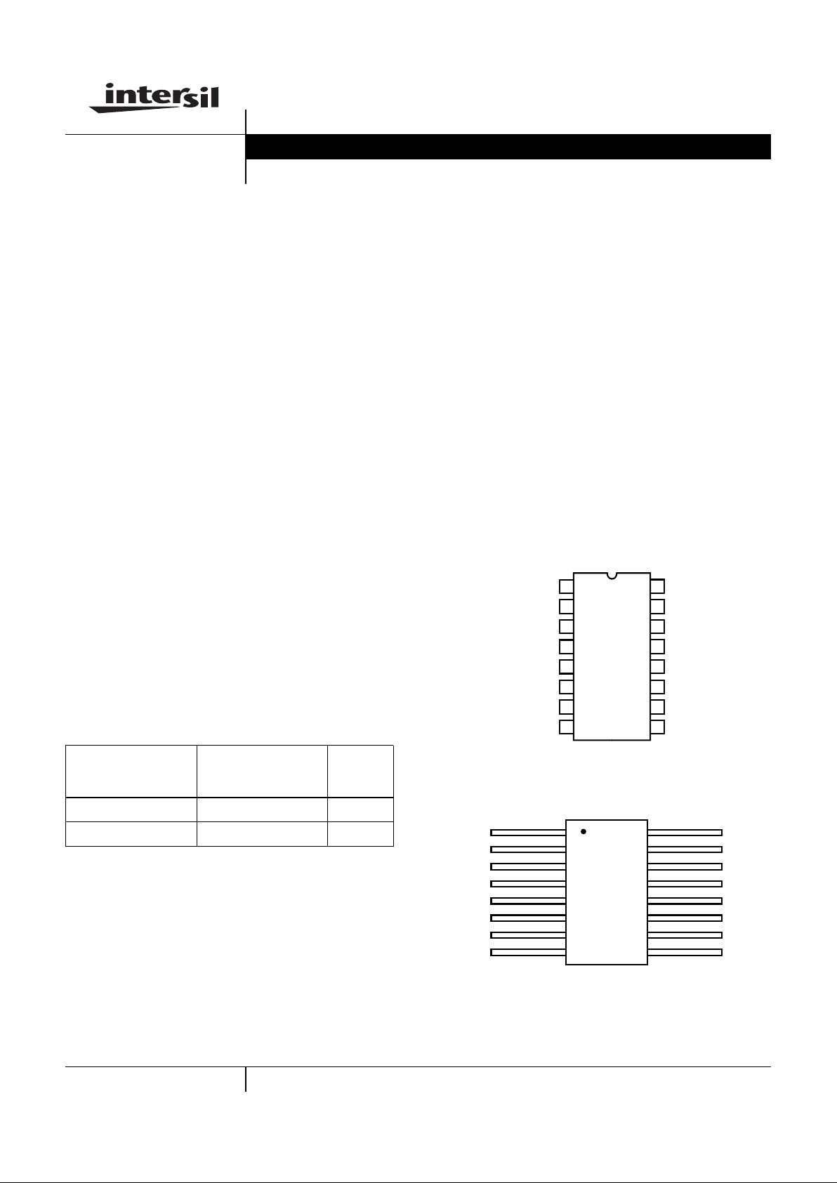
Pinouts
CD4504BT (SBDIP), CDIP2-T16
TOP VIEW
CD4504BT (FLATPACK), CDFP4-16
TOP VIEW
Ordering Information
ORDERING
NUMBER
PART
NUMBER
TEMP.
RANGE
(oC)
5962R9666501TEC CD4504BDTR -55 to 125
5962R9666501TXC CD4504BKTR -55 to 125
NOTE:
Minimumorderquantity for -T is 150 units through
distribution, or 450 units direct.
14
15
16
9
13
12
11
10
1
2
3
4
5
7
6
8
V
CC
A
OUT
A
IN
B
OUT
B
IN
C
OUT
V
SS
C
IN
V
DD
F
IN
SELECT
E
OUT
E
IN
D
OUT
D
IN
F
OUT
V
CC
A
OUT
A
IN
B
OUT
B
IN
C
OUT
C
IN
V
SS
2
3
4
5
6
7
8
116
15
14
13
12
11
10
9
V
DD
F
OUT
F
IN
SELECT
E
OUT
E
IN
D
OUT
D
IN
Data Sheet July 1999 File Number
4623.1
Page 2
2
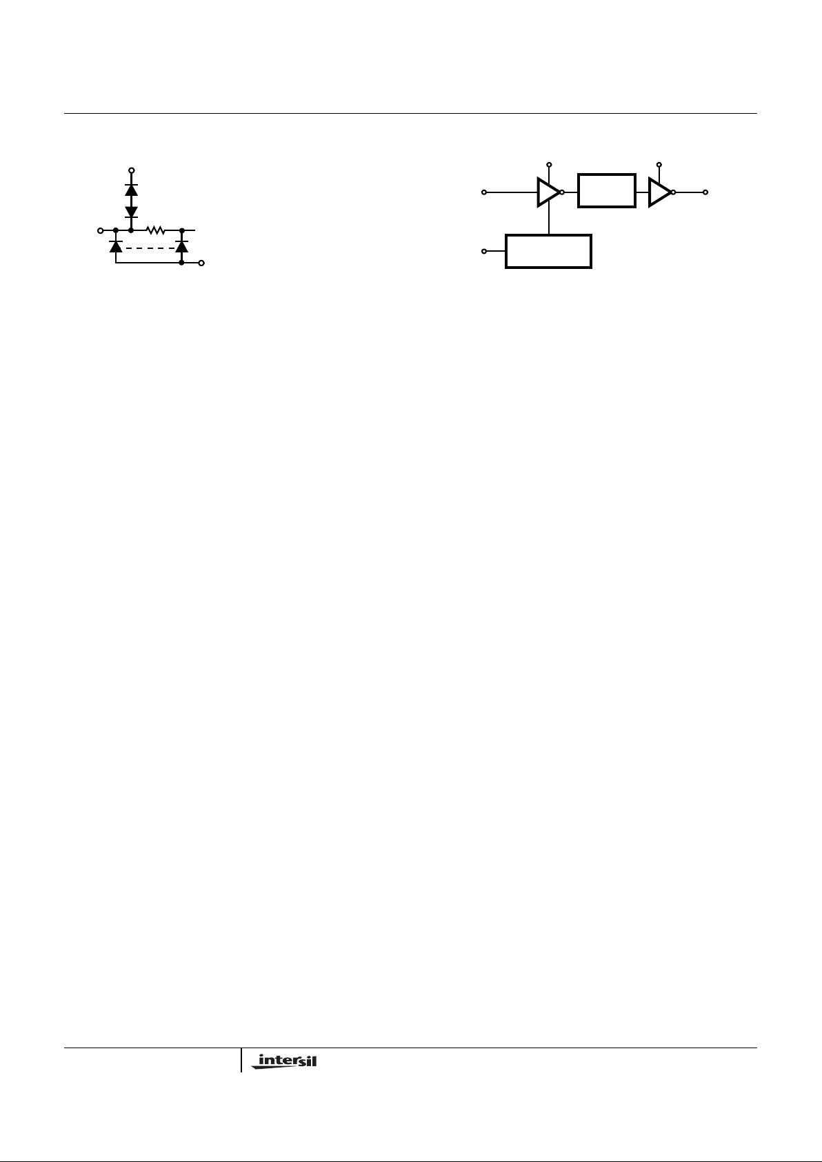
Functional Diagram
TTL/CMOS
MODE SELECT
LEVEL
SHIFTER
OUT
(2, 4, 6, 10, 12, 15)(3, 5, 7, 9, 11, 14)
† IN
†
13
SELECT
V
CC
= PIN 1
V
DD
= PIN 16
V
SS
= PIN 8
V
DD
V
SS
†
ALL INPUTS ARE PROTECTED
BY CMOS PROTECTION
NETWORK
V
CC
V
DD
CD4504BT
Page 3

3
All Intersil semiconductor products are manufactured, assembled and tested under ISO9000 quality systems certification.
Intersil semiconductor products are sold by description only. Intersil Corporation reserves the right to make changes in circuit design and/or specifications at any time without notice. Accordingly, the reader is cautioned to verify that data sheets are current before placing orders. Information furnished by Intersil is believed to be accurate and
reliable. However,no responsibility is assumed by Intersil or its subsidiaries for its use; nor for any infringements of patents or other rights of third parties which may result
from its use. No license is granted by implication or otherwise under any patent or patent rights of Intersil or its subsidiaries.
For information regarding Intersil Corporation and its products, see web site http://www.intersil.com
Sales Office Headquarters
NORTH AMERICA
Intersil Corporation
P. O. Box 883, Mail Stop 53-204
Melbourne, FL 32902
TEL: (407) 724-7000
FAX: (407) 724-7240
EUROPE
Intersil SA
Mercure Center
100, Rue de la Fusee
1130 Brussels, Belgium
TEL: (32) 2.724.2111
FAX: (32) 2.724.22.05
ASIA
Intersil (Taiwan) Ltd.
7F-6, No. 101 Fu Hsing North Road
Taipei, Taiwan
Republic of China
TEL: (886) 2 2716 9310
FAX: (886) 2 2715 3029
Die Characteristics
DIE DIMENSIONS:
(2540µm x 1753µm x 533µm ±25.4µm)
100 x 69 x 21mils ±1mil
METALLIZATION:
Type: Al
Thickness: 12.5k
Å ±1.5kÅ
SUBSTRATE POTENTIAL:
Leave Floating or Tie to V
DD
Bond Pad #16 (VDD) First
BACKSIDE FINISH:
Silicon
PASSIVATION:
Type: Phosphorus Doped Silox (S
iO2
)
Thickness: 13.0k
Å ±2.6kÅ
WORST CASE CURRENT DENSITY:
< 2.0e5 A/cm
2
TRANSISTOR COUNT:
72
PROCESS:
Bulk CMOS
Metallization Mask Layout
CD4504BT
69mils
100mils
CD4504BT
 Loading...