

Page 1
October 1987
Revised January 1999
CD4503BC Hex Non-In verting 3-STATE Buffer
© 1999 Fairchild Semiconductor Corporation DS005989.prf www.fairchildsemi.com
CD4503BC
Hex Non-In verting 3-STATE Buffer
General Description
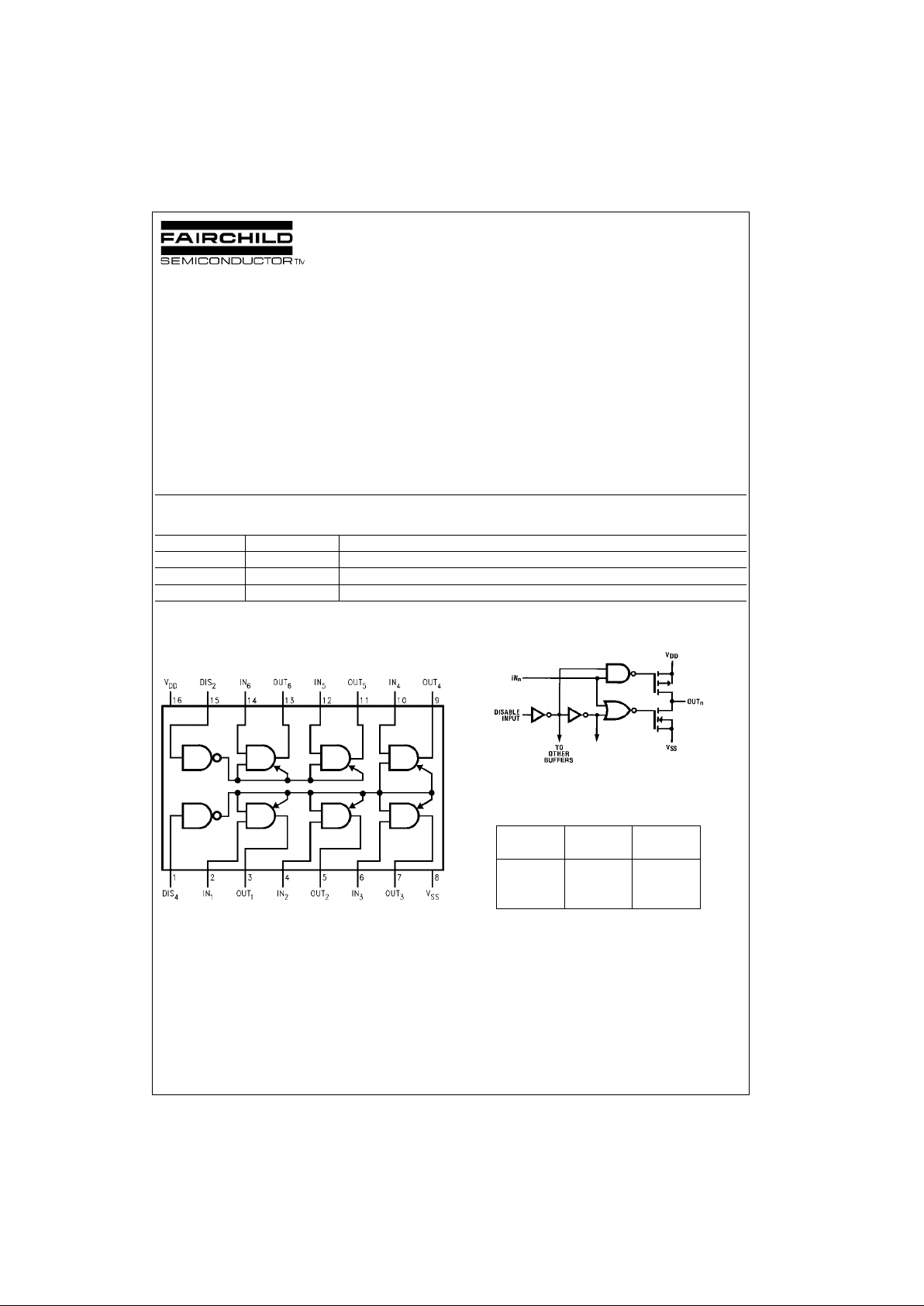
The CD4503BC is a hex non- invert ing 3-S TATE buffer with
high output current sink and source capability. 3-STATE
outputs make it useful in bus-oriented applications. Two
separate disable inputs are provide d. Buffers 1 through 4
are controlled by the disable 4 inpu t. Buffers 5 and 6 are
controlled by the disable 2 input. A high level on either disable input will cause those gates on its control lin e to go
into a high impedance state.
Features
■ Wide supply voltage range: 3.0 VDC to 18 V
DC
■ 3-STATE outputs
■ Symmetrical turn on/turn off delays
■ Symmetrical output rise and fall times
■ Pin-for-pin replacement for MM80C97 and MC14503
Ordering Code:
Devices also available in Tape and Reel. Specify by appending suffix letter “X” to the or dering code.
Connection Diagram
Pin Assignments for DIP, SOIC and SOP
Top View
Schematic Diagram
Truth Table
X = Don't Care
Order Number Package Number Package Description
CD4503BCM M16A 16-Lead Small Outline Integrated Circuit (SOIC), JEDEC MS-012, 0.150” Narrow Body
CD4503BCSJ M16D 16-Lead Small Outline Package (SOP), EIAJ TYPE II, 5.3mm Wide
CD4503BCN N16E 16-Lead Plastic Dual-In-Line Package (PDIP), JEDEC MS-001, 0.300” Wide
In Disable Out
Input
0 00
10 1
X13-STATE
Page 2
www.fairchildsemi.com 2
CD4503BC
Absolute Maximum Ratings(Note 1)
(Note 2)
Recommended Operating
Conditions
(Note 2)
Note 1: “Absolute Maxi mum Ratings” are those valu es beyond which the
safety of the device cannot be guaranteed. They are not meant to imply
that the devices should be o perated at these lim its. The table s of “Recom mended Operating Conditions” and “Electrical Cha rac t eristics” provide conditions for actual device operation.
Note 2: V
SS
= 0V unless otherw is e s pecified.
DC Electrical Characteristics (Note 2)
Note 3: IOH and IOL are tested one output at a time.
Supply Voltage (VDD) −0.5V to +18V
Input Voltage (V
IN
) −0.5V to +0.5V
Storage Temperature Range (T
S
) −65°C to +150°C
Power Dissipation (P
D
)
Dual-In-Line 700 mW
Small Outline 500 mW
Lead Temperature (T
L
)
(Soldering, 10 seconds) 260°C
Supply Voltage (V
DD
) +3V to +15V
Operating Temperature Range (T
A
) −40°C to +85°C
Symbol Parameter Conditions
−40°C +25°C +85°C
Units
Min Max Min Typ Max Min Max
I
DD
Quiescent Device VDD = 5V, 4 4 30 µA
Current VIN = VDD or V
SS
VDD = 10V, 8 8 60 µA
VIN = VDD or V
SS
VDD = 15V, 16 16 120 µA
VIN = VDD or V
SS
V
OL
LOW Level VIN = VDD or 0
Output Voltage VDD = 5V 0.05 0 0.05 0.05 V
VDD = 10V 0.05 0 0.05 0.05 V
VDD = 15V 0.05 0 0.05 0.05 V
V
OH
HIGH Level VIN = V
DD
or 0
Output Voltage VDD = 5V 4.95 4.95 4.95 V
VDD = 10V 9.95 9.95 9.95 V
VDD = 15V 14.95 14.95 14.95 V
V
IL
LOW Level VDD = 5V, 1.5 2.25 1.5 1.5 V
Input Voltage VO = 4.5V or 0.5V
VDD = 10V, 3.0 4.50 3.0 3.0 V
VO = 9.0V or 1.0V
VDD = 15V, 4.0 6.75 4.0 4.0 V
VO = 13.5V or 1.5V
V
IH
HIGH Level VDD = 5V, 3.5 3.5 2.75 3.5 V
Input Voltage VO = 0.5V or 4.5V
VDD = 10V, 7.0 7.0 5.5 7.0 V
VO = 1.0V or 9.0V
VDD = 15V, 11.0 11.0 8.25 11.0 V
VO = 1.5V or 13.5V
I
OL
LOW Level Output VDD = 4.5V, VOL = 0.4V 2.30 1.95 2.65 1.60 mA
Current VDD = 5.0V, VOL = 0.4V 2.5 2.10 2.75 1.75 mA
VDD = 10V, V
OL
= 0.5V 6.5 5.45 7.0 4.45 mA
VDD = 15V, VOL = 1.5V 16.50 13.80 25.00 11.30 mA
I
OH
HIGH Level Output VDD = 5V, VOH = 4.6V −1.04 −0.88 −1.76 −0.7 mA
Current VDD = 10V, VOH = 9.5V −2.60 −2.2 −4.50 −1.8 mA
VDD = 15V, VOH = 13.5V −7.2 −6.0 −17.6 −4.8 mA
I
TL
3-STATE Leakage Current VDD = 15V ±0.3 ±10−4 ±0.3 ±1.0 µA
I
IN
Input Current VDD = 15V ±0.3 ±10−5±0.3 ±1.0 µA
Page 3

3 www.fairchildsemi.com
CD4503BC
AC Electrical Characteristics (Note 4)
TA = 25°C, CL = 50 pF, RL = 200 kΩ, Input tr = tf = 20 ns, unless otherwise specified
Note 4: AC Parameters are guaranteed by DC correlated testin g.
Symbol Parameter Conditions Min Typ Max Units
t
PHL
, t
PLH
Propagation Delay Time VDD = 5V 75 100 ns
VDD = 10V 35 40 ns
VDD = 15V 25 30 ns
t
PLZ
, t
PHZ
Propagation Delay Time, VDD = 5V 80 125 ns
Logical Level to HIGH VDD = 10V 40 90 ns
Impedance State VDD = 15V 35 70 ns
t
PZL
, t
PZH
Propagation Delay Time, VDD = 5V 95 175 ns
High Impedance State to VDD = 10V 40 80 ns
Logical Level VDD = 15V 35 70 ns
t
TLH
Output Rise Time VDD = 5V 45 80 ns
VDD = 10V 23 40 ns
VDD = 15V 18 35 ns
t
THL
Output Fall Time VDD = 5V 45 80 ns
VDD = 10V 23 40 ns
VDD = 15V 18 35 ns
Page 4

www.fairchildsemi.com 4
CD4503BC
AC Test Circuits and Switching Time Waveforms
t
PHL
, t
PLH
CMOS to CMOS
t
PHZ
and t
PZH
t
PLZ
and t
PZL
t
PHZ
t
PLZ
t
PZH
Note: Delays measured with inp ut tr, tf ≤ 20 ns.
t
PZL
Page 5

5 www.fairchildsemi.com
CD4503BC
Physical Dimensions inches (millimeters) unless otherwise noted
16-Lead Small Outline Integrated Circuit (SOIC), JEDEC MS-012, 0.150” Narrow
Package Number M16A
16-Lead Small Outline Package (SOP), EIAJ TYPE II, 5.3mm Wide
Package Number M16D
Page 6

Fairchild does not assume any responsibility for use of any circuitry described, no circuit patent licenses are implied and Fairchild reserves the right at any time without notice to change said circuitry and specifications.
CD4503BC Hex Non-Inverting 3-STATE Buffer
LIFE SUPPORT POLICY
FAIRCHILD’S PRODUCTS ARE NOT AUTHORIZED FOR USE AS CRITICAL COMPONENTS IN LIFE SUPPORT
DEVICES OR SYSTEMS WITHOUT THE EXPRESS WRITTEN APPROVAL OF THE PRESIDENT OF FAIRCHILD
SEMICONDUCTOR CORPORATION. As used herein:
1. Life support devices or system s ar e devices or syste ms
which, (a) are intended for surgical implant into the
body, or (b) support or sustain life, and (c) whose failure
to perform when properly used in accordance with
instructions for use provided in the labeling, can be reasonably expected to result in a significant injury to the
user.
2. A critical component in any c omponent of a life suppor t
device or system whose failure to perform can be reasonably expected to cause the failure of the life suppor t
device or system, or to affect its safety or effectiveness.
www.fairchildsemi.com
Physical Dimensions inches (millimeters) unless otherwise noted (Continued)
16-Lead Plastic Dual-In-Line Package (PDIP), JEDEC MS-001, 0.300” Wide
Package Number N16E
 Loading...