

Page 1
CD4098BMS
December 1992
Features
• High Voltage Type (20V Rating)
• Retriggerable/Resettable Capability
• Trigger and Reset Propagation Delays Independent of
RX, CX
• Triggering from Leading or Trailing Edge
• Q and
• Separate Resets
• Wide Range of Output Pulse Widths
• 100% Tested for Quiescent Current at 20V
• 5V, 10V and 15V Parametric Ratings
• Standardized Symmetrical Output Characteristics
• Maximum Input Current of 1µA at 18V Over Full Pack-
• Noise Margin (Over Full Package/Temperature Range)
• Meets All Requirements of JEDEC Tentative Standard
Q Buffered Outputs Available
age Temperature Range; 100nA at 18V and +25
- 1V at VDD = 5V
- 2V at VDD = 10V
- 2.5V at VDD = 15V
No. 13B, “Standard Specifications for Description of
‘B’ Series CMOS Devices”
CMOS Dual Monostable Multivibrator
Description
CD4098BMS dual monostable multivibrator provides stable
retriggerable/resettable one shot operation for any fixed voltage timing application.
An external resistor (RX) and an external capacitor (CX)
control the timing for the circuit. Adjustment of RX and CX
provides a wide range of output pulse widths from the Q and
Q terminals. The time delay from trigger input to output
transition (trigger propagation delay) and the time delay from
reset input to output transition (reset propagation delay) are
independent of RX and CX.
Leading edge triggering (+TR) and trailing edge triggering
(-TR) inputs are provided for triggering from either edge of
an input pulse. An unused +TR input should be tied to VSS.
An unused -TR input should be tied to VDD. A RESET (on
low level) is provided for immediate termination of the output
o
C
pulse or to prevent output pulses when power is turned on.
An unused RESET input should be tied to VDD. However, if
an entire section of the CD4098BMS is not used, its RESET
should be tied to VSS. See Table 9.
In normal operation the circuit triggers (extends the output
pulse one period) on the application of each new trigger
pulse. For operation in the non-retriggerable mode,
Q is
connected to -TR when leading edge triggering (+TR) is
used or Q is connected to +TR when trailing edge triggering
(-TR) is used.
Applications
• Pulse Delay and Timing
• Pulse Shaping
Astable Multivibrator
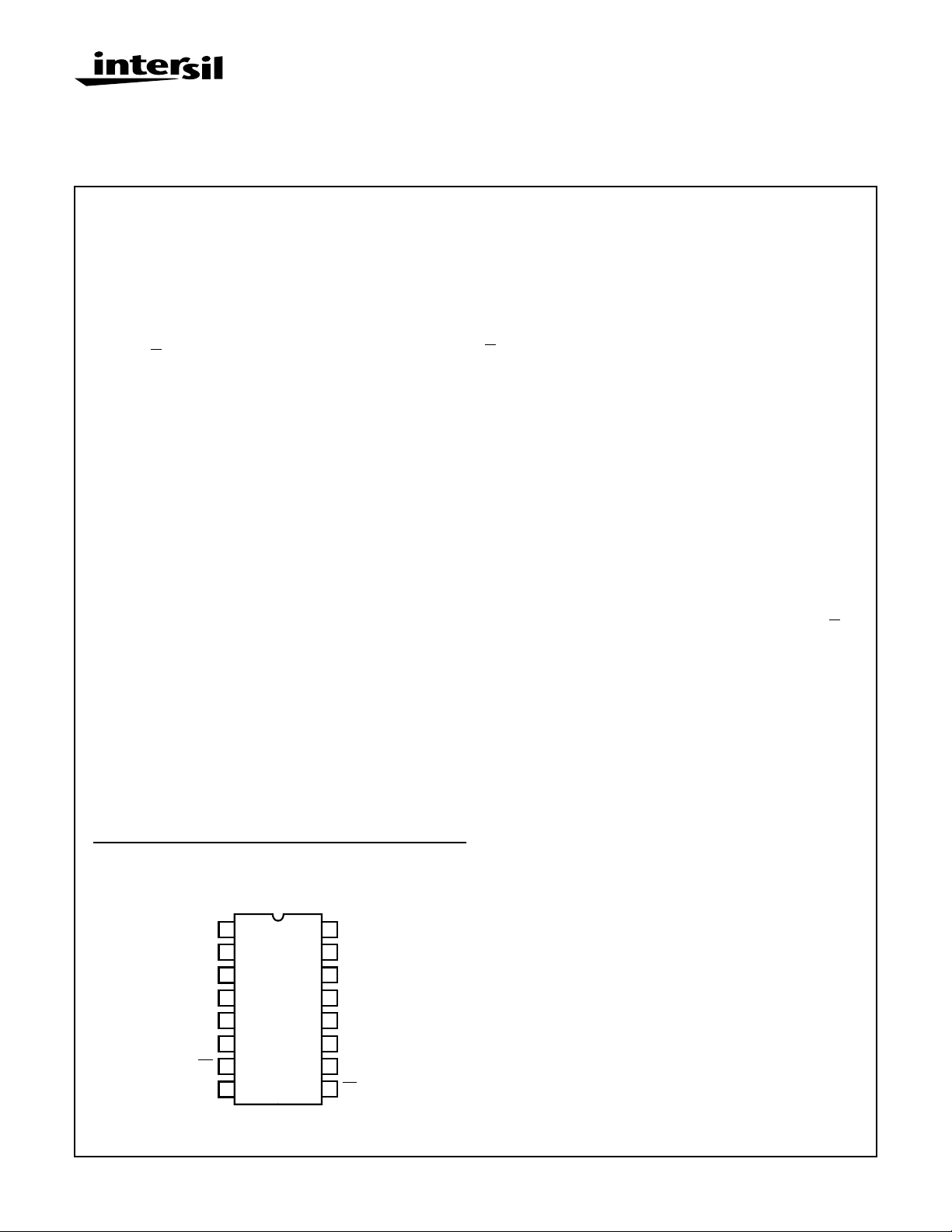
Pinout
CD4098BMS
TOP VIEW
1
CX1
-TR (1)
Q1
Q1
VSS
2
3
4
5
6
7
8
RXCX (1)
RESET (1)
+TR (1)
TERMINALS 1, 8, 15 ARE ELECTRICALLY
CONNECTED INTERNALLY
VDD
16
15
CX2
RXCX (2)
14
RESET (2)
13
+TR (2)
12
-TR (2)
11
Q2
10
9
Q2
The time period (T) for this multivibrator can be
approximated by: TX =
1
/2RXCX for CX 3 0.01µF. Time
periods as a function of RX for values of CX and VDD are
given in Figure 8. Values of T vary from unit to unit and as a
function of voltage, temperature, and RXCX.
The minimum value of external resistance, RX, is 5kΩ. The
maximum value of external capacitance, CX, is 100µF.
Figure 9 shows time periods as a function of CX for values of
RX and VDD.
The output pulse width has variations of ±2.5% typically , over
the temperature range of -55
o
C to +125oC for CX = 1000pF
and RX = 100kΩ.
For power supply variations of ±5%, the output pulse width
has variations of ±0.5% typically, for VDD = 10V and 15V
and ±1% typically, for VDD = 5V at CX = 1000pF and
RX = 5kΩ.
The CD4098BMS is supplied in these 16-lead outline packages:
Braze Seal DIP H4T
Frit Seal DIP H1F
Ceramic Flatpack H6W
CAUTION: These devices are sensitive to electrostatic discharge; follow proper IC Handling Procedures.
1-888-INTERSIL or 321-724-7143 | Copyright © Intersil Corporation 1999
7-482
File Number
3332
Page 2

Functional Diagram
CD4098BMS
+TR
-TR
RESET
+TR
-TR
RESET
VDD = 16
VSS = 8
CX1
1 2 RXCX (1)
4
5
3
12
11
13
MONO 1
MONO 2
15 14 RXCX (2)
CX2
RX1
RX2
VDD
6
Q1
7
Q1
10
Q2
9
Q2
VDD
7-483
Page 3
Specifications CD4098BMS
Absolute Maximum Ratings Reliability Information
DC Supply Voltage Range, (VDD) . . . . . . . . . . . . . . . -0.5V to +20V
(Voltage Referenced to VSS Terminals)
Input Voltage Range, All Inputs . . . . . . . . . . . . .-0.5V to VDD +0.5V
DC Input Current, Any One Input . . . . . . . . . . . . . . . . . . . . . . . .±10mA
Operating Temperature Range. . . . . . . . . . . . . . . . -55
Package Types D, F, K, H
Storage Temperature Range (TSTG). . . . . . . . . . . -65
o
C to +125oC
o
C to +150oC
Lead Temperature (During Soldering) . . . . . . . . . . . . . . . . . +265
At Distance 1/16 ± 1/32 Inch (1.59mm ± 0.79mm) from case for
10s Maximum
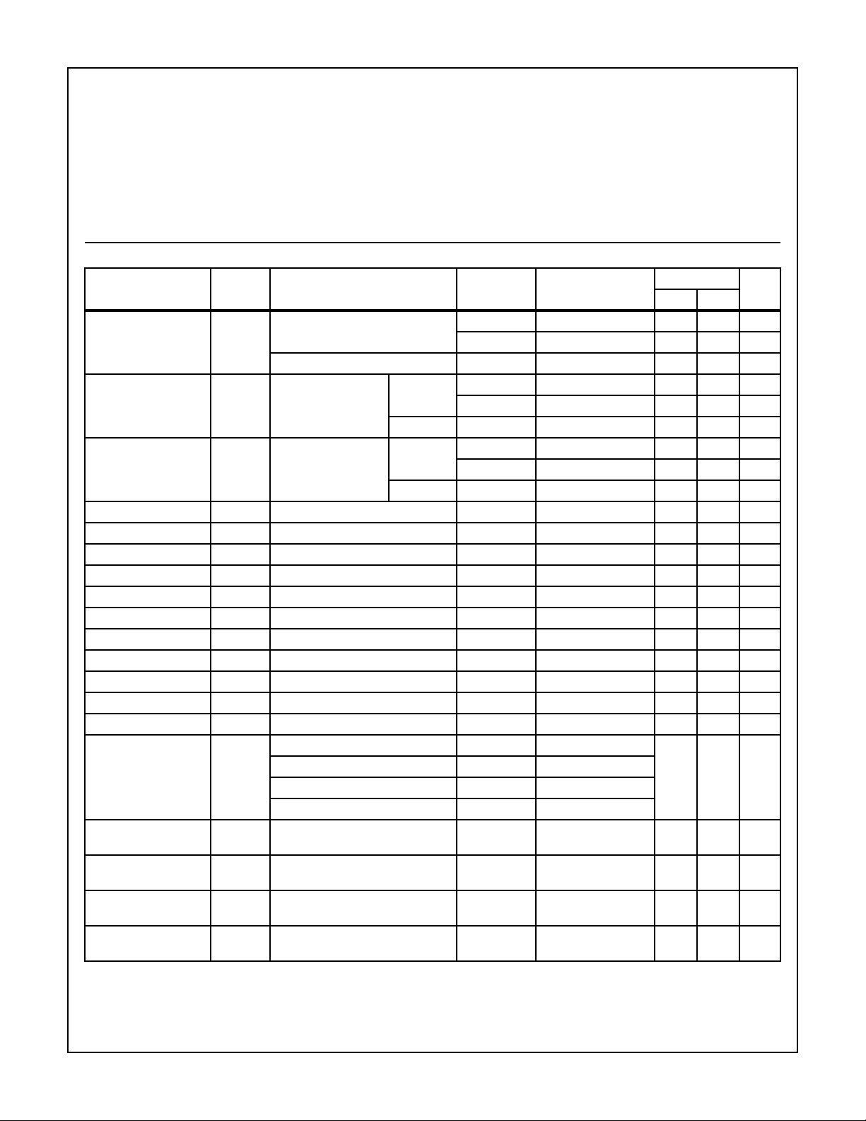
TABLE 1. DC ELECTRICAL PERFORMANCE CHARACTERISTICS
PARAMETER SYMBOL CONDITIONS (NOTE 1)
Supply Current IDD VDD = 20V, VIN = VDD or GND 1 +25
VDD = 18V, VIN = VDD or GND 3 -55oC-2µA
Input Leakage Current IIL VIN = VDD or GND VDD = 20V 1 +25
VDD = 18V 3 -55oC -100 - nA
Input Leakage Current IIH VIN = VDD or GND VDD = 20V 1 +25oC - 100 nA
VDD = 18V 3 -55oC - 100 nA
Output Voltage VOL15 VDD = 15V, No Load 1, 2, 3 +25oC, +125oC, -55oC - 50 mV
Output Voltage VOH15 VDD = 15V, No Load (Note 3) 1, 2, 3 +25oC, +125oC, -55oC 14.95 - V
Output Current (Sink) IOL5 VDD = 5V, VOUT = 0.4V 1 +25oC 0.53 - mA
Output Current (Sink) IOL10 VDD = 10V, VOUT = 0.5V 1 +25oC 1.4 - mA
Output Current (Sink) IOL15 VDD = 15V, VOUT = 1.5V 1 +25oC 3.5 - mA
Output Current (Source) IOH5A VDD = 5V, VOUT = 4.6V 1 +25oC - -0.53 mA
Output Current (Source) IOH5B VDD = 5V, VOUT = 2.5V 1 +25oC - -1.8 mA
Output Current (Source) IOH10 VDD = 10V, VOUT = 9.5V 1 +25oC - -1.4 mA
Output Current (Source) IOH15 VDD = 15V, VOUT = 13.5V 1 +25oC - -3.5 mA
N Threshold Voltage VNTH VDD = 10V, ISS = -10µA 1 +25oC -2.8 -0.7 V
P Threshold Voltage VPTH VSS = 0V, IDD = 10µA 1 +25oC 0.7 2.8 V
Functional F VDD = 2.8V, VIN = VDD or GND 7 +25oC VOH >
VDD = 20V, VIN = VDD or GND 7 +25oC
VDD = 18V, VIN = VDD or GND 8A +125oC
VDD = 3V, VIN = VDD or GND 8B -55oC
Input Voltage Low
VIL VDD = 5V, VOH > 4.5V, VOL < 0.5V 1, 2, 3 +25oC, +125oC, -55oC - 1.5 V
(Note 2)
Input Voltage High
VIH VDD = 5V, VOH > 4.5V, VOL < 0.5V 1, 2, 3 +25oC, +125oC, -55oC 3.5 - V
(Note 2)
Input Voltage Low
(Note 2)
Input Voltage High
(Note 2)
VIL VDD = 15V, VOH > 13.5V,
VOL < 1.5V
VIH VDD = 15V, VOH > 13.5V,
VOL < 1.5V
NOTES: 1. All voltages referenced to device GND, 100% testing being
implemented.
2. Go/No Go test with limits applied to inputs.
Thermal Resistance . . . . . . . . . . . . . . . . θ
Ceramic DIP and FRIT Package. . . . . 80oC/W 20oC/W
Flatpack Package . . . . . . . . . . . . . . . . 70
Maximum Package Power Dissipation (PD) at +125oC
For TA = -55
For TA = +100
o
C
Device Dissipation per Output Transistor . . . . . . . . . . . . . . . 100mW
o
C to +100oC (Package Type D, F, K). . . . . . 500mW
o
C to +125oC (Package Type D, F, K) . . . . .Derate
Linearity at 12mW/oC to 200mW
ja
o
C/W 20oC/W
For TA = Full Package Temperature Range (All Package Types)
Junction Temperature . . . . . . . . . . . . . . . . . . . . . . . . . . . . . . +175oC
GROUP A
LIMITS
SUBGROUPS TEMPERATURE
o
C-2µA
2 +125oC - 200 µA
o
C -100 - nA
2 +125oC -1000 - nA
2 +125oC - 1000 nA
VOL <
VDD/2
VDD/2
1, 2, 3 +25oC, +125oC, -55oC- 4 V
1, 2, 3 +25oC, +125oC, -55oC11 - V
3. For accuracy, voltage is measured differentially to VDD. Limit
is 0.050V max.
θ
jc
UNITSMIN MAX
V
7-484
Page 4
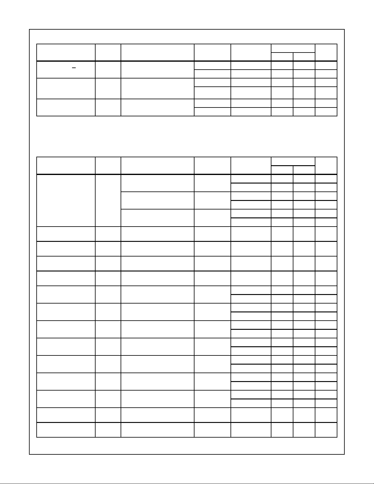
Specifications CD4098BMS
TABLE 2. AC ELECTRICAL PERFORMANCE CHARACTERISTICS
GROUP A
PARAMETER SYMBOL CONDITIONS (NOTE 1, 2)
Propagation Delay
+TR, -TR to Q, Q
TPHL1
TPLH1
VDD = 5V, VIN = VDD or GND
RX = 5K to 10KΩ, CX ≥ 15pF
Transition Time TTHL1 VDD = 5V, VIN = VDD or GND
RX = 5K to 10KΩ, CX = 15pF to
10,000pF
Transition Time
(Note 2)
TTLH1 VDD = 5V, VIN = VDD or GND
RX = 5K to 10KΩ, CX ≥ 15pF
NOTES:
1. CL = 50pF, RL = 200K, Input TR, TF < 20ns.
2. -55oC and +125oC limits guaranteed, 100% testing being implemented.
TABLE 3. ELECTRICAL PERFORMANCE CHARACTERISTICS
PARAMETER SYMBOL CONDITIONS NOTES TEMPERATURE
Supply Current IDD VDD = 5V, VIN = VDD or GND 1, 2 -55
VDD = 10V, VIN = VDD or GND 1, 2 -55
VDD = 15V, VIN = VDD or GND 1, 2 -55
Output Voltage VOL VDD = 5V, No Load 1, 2 +25
Output Voltage VOL VDD = 10V, No Load 1, 2 +25
Output Voltage VOH VDD = 5V, No Load 1, 2 +25
Output Voltage VOH VDD = 10V, No Load 1, 2 +25
Output Current (Sink) IOL5 VDD = 5V, VOUT = 0.4V 1, 2 +125
Output Current (Sink) IOL10 VDD = 10V, VOUT = 0.5V 1, 2 +125
Output Current (Sink) IOL15 VDD = 15V, VOUT = 1.5V 1, 2 +125
Output Current (Source) IOH5A VDD = 5V, VOUT = 4.6V 1, 2 +125
Output Current (Source) IOH5B VDD = 5V, VOUT = 2.5V 1, 2 +125
Output Current (Source) IOH10 VDD = 10V, VOUT = 9.5V 1, 2 +125
Output Current (Source) IOH15 VDD =15V, VOUT = 13.5V 1, 2 +125
Input Voltage Low VIL VDD = 10V, VOH > 9V, VOL <
1V
Input Voltage High VIH VDD = 10V, VOH > 9V, VOL <
1V
SUBGROUPS TEMPERATURE
9 +25oC - 500 ns
10, 11 +125oC, -55oC - 675 ns
9 +25oC - 200 ns
10, 11 +125oC, -55oC - 270 ns
9 +25oC - 200 ns
10, 11 +125oC, -55oC - 270 ns
o
+125
o
+125
o
+125
o
C, +125oC,
-55oC
o
C, +125oC,
-55oC
o
C, +125oC,
-55oC
o
C, +125oC,
-55oC
-55
-55
-55
-55
-55
-55
-55
o
1, 2 +25
C, +125oC,
-55oC
o
1, 2 +25
C, +125oC,
-55oC
LIMITS
UNITSMIN MAX
LIMITS
UNITSMIN MAX
C, +25oC- 1 µA
o
C-30µA
C, +25oC- 2 µA
o
C-60µA
C, +25oC- 2 µA
o
C - 120 µA
-50mV
-50mV
4.95 - V
9.95 - V
o
C 0.36 - mA
o
C 0.64 - mA
o
C 0.9 - mA
o
C 1.6 - mA
o
C 2.4 - mA
o
C 4.2 - mA
o
C - -0.36 mA
o
C - -0.64 mA
o
C - -1.15 mA
o
C - -2.0 mA
o
C - -0.9 mA
o
C - -1.6 mA
o
C - -2.4 mA
o
C - -4.2 mA
-3V
+7 - V
7-485
Page 5

Specifications CD4098BMS
TABLE 3. ELECTRICAL PERFORMANCE CHARACTERISTICS
(Continued)
LIMITS
PARAMETER SYMBOL CONDITIONS NOTES TEMPERATURE
Propagation Delay
+TR, -TR to Q, Q
CX ≥ 15pF
Propagation Delay
Reset CX ≥ 15pF
TPHL1
TPLH1
TPHL2
TPLH2
VDD = 10V 1, 2, 3, 4 +25oC - 250 ns
VDD = 15V 1, 2, 3, 4 +25
VDD = 5V 1, 2, 3 +25oC - 450 ns
VDD = 10V 1, 2, 3, 4 +25
VDD = 15V 1, 2, 3,4 +25
Transition Time
CX = 15pF to 10,000pF
Transition Time
CX = 0.01µF to 0.1µF
TTHL1 VDD = 10V 1, 2, 3, 4 +25
VDD = 15V 1, 2, 3, 4 +25
TTLH2
TTHL2
VDD = 5V 1, 2, 3 +25
VDD = 10V 1, 2, 3, 5 +25
VDD = 15V 1, 2, 3, 5 +25
Transition Time
CX = 0.1µF to 1µF
TTHL3 VDD = 5V 1, 2, 3 +25
VDD = 10V 1, 2, 3, 4 +25
VDD = 15V 1, 2, 3, 4 +25
Transition Time
CX ≥ 15pF
Minimum Reset Pulse
Width, CX = 15pF
TTLH1 VDD = 10V 1, 2, 3, 4 +25
VDD = 15V 1, 2, 3, 4 +25
TW VDD = 5V 1, 2, 3, 5 +25
VDD = 10V 1, 2, 3, 5 +25
VDD = 15V 1, 2, 3, 5 +25
Minimum Reset Pulse
Width, CX = 1000pF
TW VDD = 5V 1, 2, 3, 5 +25
VDD = 10V 1, 2, 3, 5 +25
VDD = 15V 1, 2, 3,5 +25
Minimum Reset Pulse
Width, CX = 0.1µF
TW VDD = 5V 1, 2, 3, 5 +25
VDD = 10V 1, 2, 3, 5 +25
VDD = 15V 1, 2, 3, 5 +25
Pulse Width Match Between Circuits in Same
Package
TW VDD = 5V 1, 2, 3, 6 +25
VDD = 10V 1, 2, 3, 6 +25
VDD = 15V 1, 2, 3, 6 +25
Trigger Rise or Fall Time TRTR
VDD = 5V to 15V 1, 2 +25
o
C - 200 ns
o
C - 250 ns
o
C - 150 ns
o
C - 100 ns
o
C - 80 ns
o
C - 300 ns
o
C - 150 ns
o
C - 130 ns
o
C - 500 ns
o
C - 300 ns
o
C - 160 ns
o
C - 100 ns
o
C - 80 ns
o
C - 200 ns
o
C - 80 ns
o
C - 60 ns
o
C - 1200 ns
o
C - 600 ns
o
C - 500 ns
o
C-50µs
o
C-30µs
o
C-20µs
o
C - 10 %
o
C - 15 %
o
C - 15 %
o
C - 100 µs
UNITSMIN MAX
TFTR
o
Input Capacitance CIN Any Inputs 1, 2 +25
C - 7.5 pF
NOTES:
1. All voltages referenced to device GND.
2. The parameters listed on Table 3 are controlled via design or process and are not directly tested. These parameters are characterized
on initial design release and upon design changes which would affect these characteristics.
3. CL = 50pF, RL = 200K, inputs tR, tF < 20ns.
4. RX = 5K to 10MΩ.
5. RX = 100kΩ
6. RX = 10kΩ
TABLE 4. POST IRRADIATION ELECTRICAL PERFORMANCE CHARACTERISTICS
LIMITS
PARAMETER SYMBOL CONDITIONS NOTES TEMPERATURE
Supply Current IDD VDD = 20V, VIN = VDD or GND 1, 4 +25
o
C - 7.5 µA
UNITSMIN MAX
N Threshold Voltage VNTH VDD = 10V, ISS = -10µA 1, 4 +25oC -2.8 -0.2 V
7-486
Page 6

Specifications CD4098BMS
TABLE 4. POST IRRADIATION ELECTRICAL PERFORMANCE CHARACTERISTICS
LIMITS
PARAMETER SYMBOL CONDITIONS NOTES TEMPERATURE
N Threshold Voltage
Delta
P Threshold Voltage VTP VSS = 0V, IDD = 10µA 1, 4 +25oC 0.2 2.8 V
P Threshold Voltage
Delta
Functional F VDD = 18V, VIN = VDD or GND 1 +25oC VOH >
Propagation Delay Time TPHL
NOTES: 1. All voltages referenced to device GND.
2. CL = 50pF, RL = 200K, Input TR, TF < 20ns.
∆VTN VDD = 10V, ISS = -10µA 1, 4 +25oC-±1V
∆VTP VSS = 0V, IDD = 10µA 1, 4 +25oC-±1V
VOL <
VDD = 3V, VIN = VDD or GND
VDD = 5V 1, 2, 3, 4 +25oC - 1.35 x
TPLH
3. See Table 2 for +25oC limit.
4. Read and Record
TABLE 5. BURN-IN AND LIFE TEST DELTA PARAMETERS +25oC
PARAMETER SYMBOL DELTA LIMIT
Supply Current - MSI-1 IDD ± 0.2µA
Output Current (Sink) IOL5 ± 20% x Pre-Test Reading
Output Current (Source) IOH5A ± 20% x Pre-Test Reading
VDD/2
VDD/2
+25oC
Limit
UNITSMIN MAX
V
ns
TABLE 6. APPLICABLE SUBGROUPS
MIL-STD-883
CONFORMANCE GROUP
Initial Test (Pre Burn-In) 100% 5004 1, 7, 9 IDD, IOL5, IOH5A
Interim Test 1 (Post Burn-In) 100% 5004 1, 7, 9 IDD, IOL5, IOH5A
Interim Test 2 (Post Burn-In) 100% 5004 1, 7, 9 IDD, IOL5, IOH5A
PDA (Note 1) 100% 5004 1, 7, 9, Deltas
Interim Test 3 (Post Burn-In) 100% 5004 1, 7, 9 IDD, IOL5, IOH5A
PDA (Note 1) 100% 5004 1, 7, 9, Deltas
Final Test 100% 5004 2, 3, 8A, 8B, 10, 11
Group A Sample 5005 1, 2, 3, 7, 8A, 8B, 9, 10, 11
Group B Subgroup B-5 Sample 5005 1, 2, 3, 7, 8A, 8B, 9, 10, 11, Deltas Subgroups 1, 2, 3, 9, 10, 11
Subgroup B-6 Sample 5005 1, 7, 9
Group D Sample 5005 1, 2, 3, 8A, 8B, 9 Subgroups 1, 2 3
NOTE: 1. 5% Parameteric, 3% Functional; Cumulative for Static 1 and 2.
CONFORMANCE GROUPS
Group E Subgroup 2 5005 1, 7, 9 Table 4 1, 9 Table 4
METHOD GROUP A SUBGROUPS READ AND RECORD
TABLE 7. TOTAL DOSE IRRADIATION
MIL-STD-883
METHOD
PRE-IRRAD POST-IRRAD PRE-IRRAD POST-IRRAD
TEST READ AND RECORD
7-487
Page 7

Specifications CD4098BMS
TABLE 8. BURN-IN AND IRRADIATION TEST CONNECTIONS
OSCILLATOR
FUNCTION OPEN GROUND VDD 9V ± -0.5V
Static Burn-In 1
6, 7, 9, 10 1-5, 8, 11-15 16
Note 1
Static Burn-In 2
6, 7, 9, 10 1, 8, 15 2-5, 11-14, 16
Note 1
Dynamic Burn-
- 1, 4, 8, 12, 15 2, 14, 16 6, 7, 9, 10 5, 11 3, 13
In Note 1
Irradiation
2, 6, 7, 9, 10, 14 1, 8, 15 3-5, 11-13, 16
Note 2
NOTE:
1. Each pin except VDD and GND will have a series resistor of 10K ± 5%, VDD = 18V ± 0.5V
2. Each pin except VDD and GND will have a series resistor of 47K ± 5%; Group E, Subgroup 2, sample size is 4 dice/wafer, 0 failures, VDD
= 10V ± 0.5V
TABLE 9. FUNCTIONAL TERMINAL CONNECTIONS
FUNCTION
Leading Edge Trigger/
VDD TO
TERM. NO.
MONO 1 MONO 2 MONO 1 MONO 2 MONO 1 MONO 2 MONO 1 MONO 2
3, 5 11, 13 4 12
VSS TO
TERM. NO.
INPUT PULSE TO
TERM. NO.
Retriggerable
Leading Edge Trigger/
3 13 4 12 5-7 11-9
Non-Retriggerable
Trailing Edge Trigger/
313412511
Retriggerable
Trailing Edge Trigger/
3 13 5 11 4-6 12-10
Non-Retriggerable
Unused Section 5 11 3, 4 12, 13
NOTES:
1. A retriggerable one-shot multivibrator has an output pulse width which is extended one full time period (TX) after application of the last
trigger pulse. The minimum time between retriggering edges (or trigger and retrigger edges) is 40% of (TX).
2. A non-retriggerable one-shot multivibrator has a time period TX referenced from the application of the first trigger pulse.
INPUT PULSE TRAIN
50kHz 25kHz
OTHER
CONNECTIONS
RETRIGGERABLE MODE
PULSE WIDTH (+TR MODE)
NON-RETRIGGERABLE MODE
PULSE WIDTH (-TR MODE)
TX
TX
All Intersil semiconductor products are manufactured, assembled and tested under ISO9000 quality systems certification.
Intersil products are sold by description only. Intersil Corporation reserves the right to make changes in circuit design and/or specifications at any time without
notice. Accordingly, the reader is cautioned to verify that data sheets are current before placing orders. Information furnished by Intersil is believed to be accurate
and reliable. However, no responsibility is assumed by Intersil or its subsidiaries for its use; nor for any infringements of patents or other rights of third parties which
may result from its use. No license is granted by implication or otherwise under any patent or patent rights of Intersil or its subsidiaries.
For information regarding Intersil Corporation and its products, see web site http://www.intersil.com
488
Page 8

Logic Diagram
CD4098BMS
VDD
*
4 (12)
+TR
*
5 (11)
-TR
*
3 (13)
RESET
1 (15)
8
16
NOTE:
SCHEMATIC SHOWN IS
PACKAGE. TWO SETS OF TERMINAL
NUMBERS ARE SHOWN. TERMINALS
1, 8, AND 15 ARE ELECTRICALLY
CONNECTED INTERNALLY.
VSS
VDD
1
/2 OF TOTAL
DQ
C
R1 R2
*ALL INPUTS ARE PROTECTED
BY CMOS PROTECTION
NETWORK
VDD
VSS
VDD
*
RXCX
Q
Q
2 (14)
6 (10)
7 (9)
FIGURE 1. LOGIC DIAGRAM
Typical Performance Characteristics
AMBIENT TEMPERATURE (TA) = +25oC
30
25
20
15
10
5
OUTPUT LOW (SINK) CURRENT (IOL) (mA)
0 5 10 15
FIGURE 2. TYPICAL OUTPUT LOW (SINK) CURRENT
GATE-TO-SOURCE VOLT AGE (VGS) = 15V
10V
5V
DRAIN-TO-SOURCE VOLTAGE (VDS) (V)
CHARACTERISTICS
VSS
AMBIENT TEMPERATURE (TA) = +25oC
15.0
12.5
10.0
7.5
5.0
2.5
OUTPUT LOW (SINK) CURRENT (IOL) (mA)
0 5 10 15
GATE-TO-SOURCE VOLT AGE (VGS) = 15V
10V
5V
DRAIN-TO-SOURCE VOLTAGE (VDS) (V)
FIGURE 3. MINIMUM OUTPUT LOW (SINK) CURRENT
CHARACTERISTICS
7-489
Page 9

CD4098BMS
Typical Performance Characteristics (Continued)
DRAIN-TO-SOURCE VOLTAGE (VDS) (V)
0-5-10-15
AMBIENT TEMPERATURE (TA) = +25oC
GATE-TO-SOURCE VOLT AGE (VGS) = -5V
0
-5
-10
-15
-10V
-20
-25
-15V
-30
OUTPUT HIGH (SOURCE) CURRENT (IOH) (mA)
FIGURE 4. TYPICAL OUTPUT HIGH (SOURCE) CURRENT
CHARACTERISTICS
AMBIENT TEMPERATURE (TA) = +25oC
300
SUPPLY VOLT AGE (VDD) = 15V
200
10V
100
15V
PROPAGATION DELAY TIME (tPHL, tPLH) (ns)
0
20 40 60 80 100 120 140
LOAD CAPACITANCE (CL) (pF)
FIGURE 6. TYPICAL PROPAGATION DELAY TIME vs LOAD CA-
PACITANCE, TRIGGER INTO Q OUT (ALL VALUES
OF CX AND RX).
AMBIENT TEMPERATURE (TA) = +25oC
7
10
8
6
EXTERNAL RESISTANCE (RX) (Ω)
4
2
6
10
8
6
4
2
5
10
8
6
4
2
4
10
8
6
4
2
3
10
10
CX = 1000pF
-1
CX = 15pF
CX = 100pF
VDD = 3V, 5V
2468
2468
1
VDD = 5V, 10V, 15V, 18V
2468
2468
2
10
10
VDD = 3V
= 5V
= 10V, 15V, 18V
2468
3
10
CX = 0.1 µF
CX = 0.01µF
2468
4
10
10
2468
5
6
10
PULSE WIDTH (PW) (µs)
FIGURE 8. TYPICAL EXTERNAL RESISTANCE vs PULSE
WIDTH
DRAIN-TO-SOURCE VOLTAGE (VDS) (V)
0-5-10-15
AMBIENT TEMPERATURE (TA) = +25oC
0
GATE-TO-SOURCE VOLT AGE (VGS) = -5V
-5
-10V
-15V
-10
-15
FIGURE 5. MINIMUM OUTPUT HIGH (SOURCE) CURRENT
CHARACTERISTICS
AMBIENT TEMPERATURE (TA) = +25oC
200
150
SUPPLY VOLT AGE (VDD) = 5V
100
10V
50
TRANSITION TIME (tTHL, tTLH) (ns)
0
0 40 60 80 10020
5V
LOAD CAPACITANCE (CL) (pF)
FIGURE 7. TRANSITION TIME vs LOAD CAPACITANCE FOR
RX = 5kΩ-10000kΩ AND CX = 15pF-10000pF
AMBIENT TEMPERATURE (TA) = +25oC
7
10
VDD = 3V
6
10
5
10
4
10
3
10
RX = 5KΩ
2
10
EXTERNAL CAPACITANCE (CX) (pF)
= 5V
= 10V, 15V, 18V
RX = 10KΩ
RX = 100KΩ
RX =1MΩ
RX = 10MΩ
10
-1
10
110
10 10
2
3
4
10
10
5
10
PULSE WIDTH (PW) (µs)
FIGURE 9. TYPICAL EXTERNAL CAPACITANCE vs PULSE
WIDTH
OUTPUT HIGH (SOURCE) CURRENT (IOH) (mA)
6
7-490
Page 10

CD4098BMS
Typical Performance Characteristics (Continued)
5
10
8
AMBIENT TEMPERATURE (TA) = +25oC
6
CL = 50pF RX = 100KΩ
4
FREQUENCY = 100KHz
2
RISE TIME (tr), FALL (tf) = 20ns
4
10
8
6
4
2
SUPPLY VOLT AGE (VDD) = 5V
3
10
8
6
4
2
2
10
8
10V
6
4
15V
2
MINIMUM RESET PULSE WIDTH (tWR) (ns)
6
10
6
4
2
CX = 100pF
5
10
6
4
2
4
10
6
4
2
3
10
DUTY CYCLE (P100) (µW)
6
4
2
2
AVERAGE POWER - DISSIPATION FOR 100%
10
10
2468
10
FIGURE 10. TYPICAL MINIMUM RESET PULSE WIDTH vs EXTERNAL CAPACITANCE
AMBIENT TEMPERATURE (TA) = +25oC
RX = 5KΩ TO 1MΩ
CL = 50pF
1000pF
0.01µF
0.1µF
1µF
VDD = 5V
= 10V
= 15V
64218
6428
10
10
6428
2
10
6428
3
4
10
ONE-SHOT PULSE WIDTH (τm) (µs)
FIGURE 11. AVERAGE POWER DISSIPATION vs ONE-SHOT PULSE WIDTH
2468
2
10
EXTERNAL CAPACITANCE (CX) (pF)
10
To calculate average power dissipation(P)
for less than 100% duty cycle:
P100 = average power for 100% duty
cycle:
P =
(tm)
e.g. For τm = 600µs, tT = 1000µs. CX = 0.01mF
VDD = 5V
600
P1 =
(
6428
5
10
1000
2468
3
2468
4
10
P100 where τm = one shot pulse
width
τT
τT = trigger pulse period
103µW = 600µW (see dotted line on
)
graph)
5
10
τT
τm
Applications
+TR
VDD
INPUT PULSE
OUTPUT PULSE
CX1
RX1
12
4
MONO 1
5
Q
6
3
T1 T2
FIGURE 12. PULSE DELAY
7-491
VSS
VDD
-TR
CX2
15 14
11
MONO 2
12
13
RX1 CX1
T1 ≈
RX2 CX2
T2 ≈
CX ≥ 0.01µF
VDDVDD
RX2
Q
10
OUTPUT
2
2
Page 11

Applications (Continued)
CD4098BMS
VDD
SUPPLY
VDD
VDD
VSS
RESET
TO ENSURE RESTART, APPLY RESET
*
(NEGATIVE PULSE) AFTER VDD
SUPPLY VOLTAGE HAS REACHED
ITS VDD LEVEL
+TR
RUN
IDD
CX1
12
4
MONO 1
5
R
3
8
VSS
FIGURE 13. ASTABLE MULTIVIBRATOR WITH RESTART AFTER RESET CAPABILITY
VDD
RX1
6
Q1
Q1
VDD
SUPPLY
RESET
VSS
Q2
IDD
-TR
VDD
0
*
R
CX2
15 14
11
MONO 2
12
13
T2 T2T1
TX
RX2
10
IDD, TX vs RX
IDD
RX
Q2
9
Q2
OUTPUT
10MΩ
(AVG.)TX(T1 + T2) VDD
10kΩ
1mA
0.05mA
2.5mA
0.5mA
5mA
1mA
3.8µs
0.5s
3.2µs
0.5s
3µs
0.5s
5V
10V
10V
NOTES:
1. All values are typical.
2. CX range: 0.0001µF to 0.1µF
Chip Dimensions and Pad Layout
Dimensions in parenthesis are in millimeters and are
derived from the basic inch dimensions as indicated.
Grid graduations are in mils (10
METALLIZATION: Thickness: 11kÅ− 14kÅ, AL.
PASSIVATION: 10.4kÅ - 15.6kÅ, Silane
BOND PADS: 0.004 inches X 0.004 inches MIN
DIE THICKNESS: 0.0198 inches - 0.0218 inches
-3
inch).
7-492
 Loading...