

Page 1
October 1987
Revised January 1999
CD4093BC Quad 2-Input NAND Schmitt Trigger
© 1999 Fairchild Semiconductor Corporation DS005982.prf www.fairchildsemi.com
CD4093BC
Quad 2-Input NAND Schmitt Trigger
General Description
The CD4093B consists of four Schmitt-trigger circuits.
Each circ ui t f u nc t io ns as a 2- i n pu t N AN D ga te w it h Sc h mi tt trigger action on both inpu ts. The ga te switches at different
points for positive and negative-go ing signals. The differ-
ence between the posit ive (V
T
+
) and the negat ive voltage
(V
T
−
) is defined as hysteresis voltage (VH).
All outputs have equal source and sink currents and conform to standard B-series output drive (see Static Electrical
Characteristics).
Features
■ Wide supply voltage range: 3.0V to 15V
■ Schmitt-trigger on each input
with no external components
■ Noise immunity greater than 50%
■ Equal source and sink currents
■ No limit on input rise and fall time
■ Standard B-series output drive
■ Hysteresis voltage (any input) T
A
= 25°C
Applications
• Wave and pulse shapers
• High-noise-environment systems
• Monostable multivibrators
• Astable multivibrators
• NAND logic
Ordering Code:
Devices also available in Tape and Reel. Specify by appending the suffix letter “X” to the ordering code.
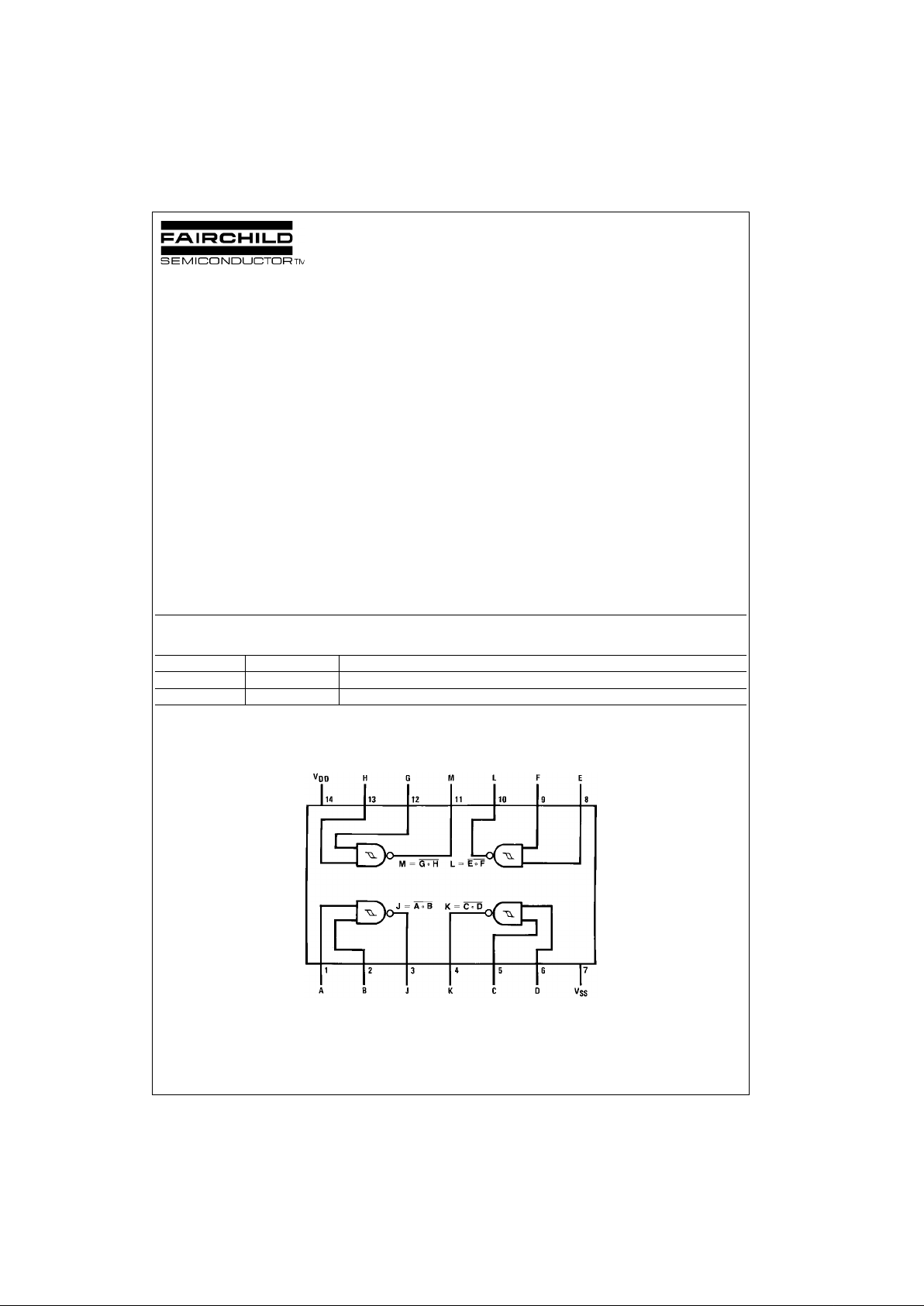
Connection Diagram
Pin Assignments for SOIC and DIP
Top View
Typical V
DD
= 5.0V VH = 1.5V
V
DD
= 10V VH = 2.2V
V
DD
= 15V VH = 2.7V
Guarant eed V
H
= 0.1 V
DD
Order Number Package Number Package Description
CD4093BCM M14A 14-Lead Small Outline Integrated Circuit (SOIC), JEDEC MS-120, 0.150” Narrow Body
CD4093BCN N14A 14-Lead Plastic Dual-In-Line Package (PDIP), JEDEC MS-001, 0.300” Wide
Page 2
www.fairchildsemi.com 2
CD4093BC
Absolute Maximum Ratings(Note 1)
(Note 2)
Recommended Operating
Conditions
(Note 2)
Note 1: “Absolute Maxi mum Ratings” are those valu es beyond which the
safety of the device cannot be guaranteed; they are not m eant to imply that
the devices should be operated at these limits. The table of “Recommended Operating Conditions” and “Electrical Characteristics” provides
conditions for actual device op eration.
Note 2: V
SS
= 0V unless otherw is e s pecified.
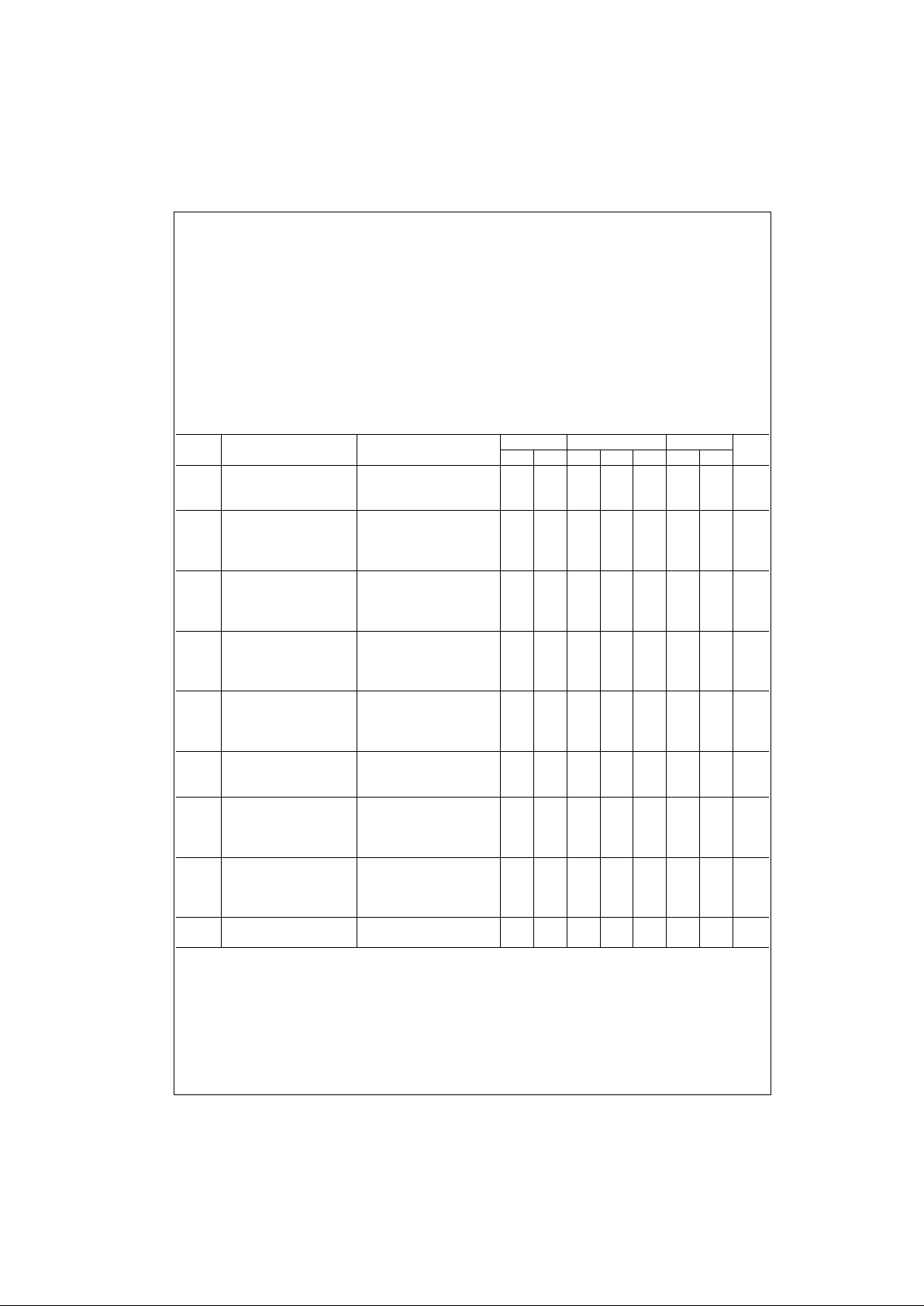
DC Electrical Characteristics (Note 2)
Note 3: IOH and IOL are tested one output at a time.
DC Supply Voltage (VDD) −0.5 to +18 V
DC
Input Voltage (VIN) −0.5 to VDD +0.5 V
DC
Storage Temperature Range (TS) −65°C to +150°C
Power Dissipation (P
D
)
Dual-In-Line 700 mW
Small Outline 500 mW
Lead Temperature (T
L
)
(Soldering, 10 seconds) 260°C
DC Supply Voltage (V
DD
) 3 to 15 V
DC
Input Voltage (VIN)0 to V
DD VDC
Operating Temperature Range (TA) −40°C to +85°C
Symbol Parameter Conditions
−40°C +25°C +85°C
Units
Min Max Min Typ Max Min Max
I
DD
Quiescent Device VDD = 5V 1.0 1.0 7.5 µA
Current VDD = 10V 2.0 2.0 15.0 µA
VDD = 15V 4.0 4.0 30.0 µA
V
OL
LOW Level VIN = V
DD,
|IO| < 1 µA
Output Voltage VDD = 5V 0.05 0 0.05 0.05 V
VDD = 10V 0.05 0 0.05 0.05 V
VDD = 15V 0.05 0 0.05 0.05 V
V
OH
HIGH Level VIN = VSS, |IO| < 1 µA
Output Voltage VDD = 5V 4.95 4.95 5 4.95 V
VDD = 10V 9.95 9.95 10 9.95 V
VDD = 15V 14.95 14.95 15 14.95 V
VT− Negative-Going Threshold |IO| < 1 µA
Voltage (Any Input) VDD = 5V, VO = 4.5V 1.3 2.25 1.5 1.8 2.25 1.5 2.3 V
VDD = 10V, VO = 9V 2.85 4.5 3.0 4.1 4.5 3.0 4.65 V
VDD = 15V, VO = 13.5V 4.35 6.75 4.5 6.3 6.75 4.5 6.9 V
VT+ Positive-Going Threshold |IO| < 1 µA
Voltage (Any Input) VDD = 5V, VO = 0.5V 2.75 3.6 2.75 3.3 3.5 2.65 3.5 V
VDD = 10V, VO = 1V 5.5 7.15 5.5 6.2 7.0 5.35 7.0 V
VDD = 15V, VO = 1.5V 8.25 10.65 8.25 9.0 10.5 8.1 10.5 V
V
H
Hysteresis (VT+ − VT−)V
DD
= 5V 0.5 2.35 0.5 1.5 2.0 0.35 2.0 V
(Any Input) VDD = 10V 1.0 4.3 1.0 2.2 4.0 0.70 4.0 V
VDD = 15V 1.5 6.3 1.5 2.7 6.0 1.20 6.0 V
I
OL
LOW Level Output VIN = V
DD
Current (Note 3) VDD = 5V, VO = 0.4V 0.52 0.44 0.88 0.36 mA
VDD = 10V, VO = 0.5V 1.3 1.1 2.25 0.9 mA
VDD = 15V, VO = 1.5V 3.6 3.0 8.8 2.4 mA
I
OH
HIGH Level Output VIN = V
SS
Current (Note 3) VDD = 5V, VO = 4.6V −0.52 0.44 −0.88 −0.36 mA
VDD = 10V, VO = 9.5V −1.3 −1.1 −2.25 −0.9 mA
VDD = 15V, VO = 13.5V −3.6 −3.0 −8.8 −2.4 mA
I
IN
Input Current VDD = 15V, VIN = 0V −0.3 −10−5−0.3 −1.0 µA
VDD = 15V, VIN = 15V 0.3 10−50.3 1.0 µA
Page 3
3 www.fairchildsemi.com
CD4093BC
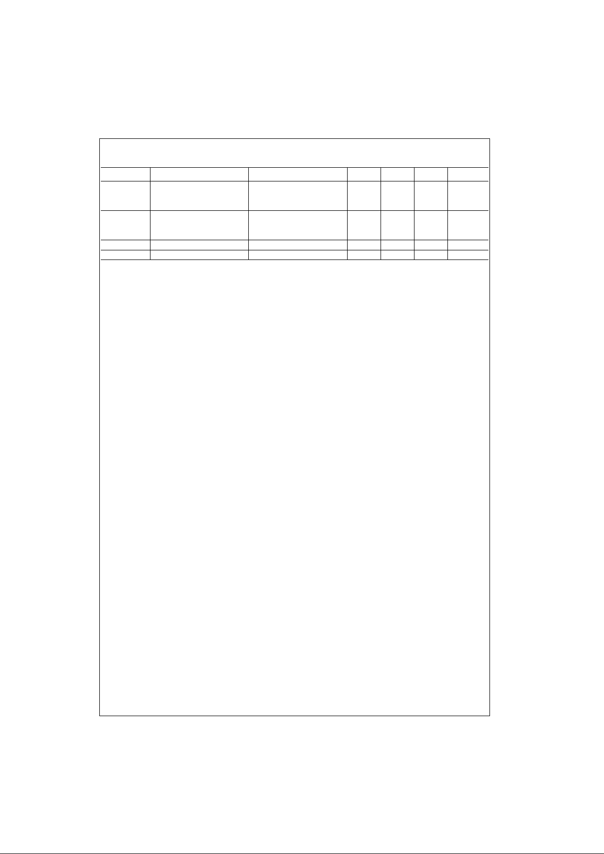
AC Electrical Characteristics (Note 4)
TA = 25°C, CL = 50 pF, RL = 200k, Input tr, tf = 20 ns, unless otherwise specified
Note 4: AC Parameters are guaranteed by DC correlated testin g.
Symbol Parameter Conditions Min Typ Max Units
t
PHL
, t
PLH
Propagation Delay Time VDD = 5V 300 450 ns
VDD = 10V 120 210 ns
VDD = 15V 80 160 ns
t
THL
, t
TLH
Transition Time VDD = 5V 90 145 ns
VDD = 10V 50 75 ns
VDD = 15V 40 60 ns
C
IN
Input Capacitance (Any Input) 5.0 7.5 pF
C
PD
Power Dissipation Capacitance (Per Gate) 24 pF
Page 4

www.fairchildsemi.com 4
CD4093BC
Typical Applications
Gated Oscillator
Assume t1 + t2 >> t
PHL
+ t
PLH
then:
t
0
= RC ln [VDD/VT−]
t
1
= RC ln [(VDD − VT−)/(VDD − VT+)]
t
2
= RC ln [V
T
+/V
T−]
Gated One-Shot
(a) Negative-Edge Triggered
(b) Positive-Edge T riggered
Page 5

5 www.fairchildsemi.com
CD4093BC
Typical Performance Characteristics
Typical Transfer
Characteristics
Guaranteed Hysteresis vs V
DD
Guaranteed Trigger Threshold
Voltage vs V
DD
Guaranteed Hysteresis vs V
DD
Input and Output Characteristics
V
NML
= V
IH(MIN)
− VOL ≅ V
IH(MIN)
= VT+
(MIN)
V
NMH
= VOH − V
IL(MAX)
≅ VDD − V
IL(MAX)
= VDD − VT−
(MAX)
Page 6

www.fairchildsemi.com 6
CD4093BC
AC Test Circuits and Switching Time Waveforms
Page 7

7 www.fairchildsemi.com
CD4093BC
Physical Dimensions inches (millimeters) unless otherwise noted
14-Lead Small Outline Integrated Circuit (SOIC), JEDEC MS-120, 0.150” Narrow Body
Package Number M14A
Page 8

Fairchild does not assume any responsibility for use of any circuitry descri bed, no circuit patent licenses are implied and Fairchil d reser ves the right at any time without notice to change said circuitr y and specifications.
CD4093BC Quad 2-Input NAND Schmitt Trigger
LIFE SUPPORT POLICY
FAIRCHILD’S PRODUCTS ARE NOT AUTHORIZED FOR USE AS CRITICAL COMPONENTS IN LIFE SUPPORT
DEVICES OR SYSTEMS WITHOUT THE EXPRESS WRITTEN APPROVAL OF THE PRESIDENT OF FAIRCHILD
SEMICONDUCTOR CORPORATION. As used herein:
1. Life support devices or system s ar e devices or syste ms
which, (a) are intended for surgical implant into the
body, or (b) support or sustain life, and (c) whose failure
to perform when properly used in accordance with
instructions for use provided in the labeling, can be reasonably expected to result in a significant injury to the
user.
2. A critical component in any c omponent of a life suppor t
device or system whose failure to perform can be reasonably expected to cause the failure of the life suppor t
device or system, or to affect its safety or effectiveness.
www.fairchildsemi.com
Physical Dimensions inches (millimeters) unless otherwise noted (Continued)
14-Lead Plastic Dual-In-Line Package (PDIP), JEDEC MS-001, 0.300” Wide
Package Number N14A
 Loading...