

Datasheet CD4066BCSJX, CD4066BCSJ, CD4066BCN, CD4066BCMX, CD4066BCM Datasheet (Fairchild Semiconductor)
...
© 2000 Fairchild Semiconductor Corporation DS005665 www.fairchildsemi.com
November 1983
Revised August 2000
CD4066BC Quad Bilateral Switch
CD4066BC
Quad Bilateral Switch
General Description
The CD4066BC is a quad bilateral switch intended for the
transmission or multiplexing of analog or digital signals. It is
pin-for-pin compatible with CD4016BC, but has a much
lower “ON” resistance, and “ON” resistance is relatively
constant over the input-signal range.
Features
■ Wide supply voltage range 3V to 15V
■ High noise immunity 0.45 V
DD
(typ.)
■ Wide range of digital and
±7.5 V
PEAK
analog switching
■ “ON” resistance for 15V operation 80
Ω
■ Matched “ON” resistance ∆R
ON
= 5Ω (typ.)
over 15V signal input
■ “ON” resistance flat over peak-to -p eak si gna l range
■ High “ON”/“OFF” 65 dB (typ.)
output voltage ratio @ f
is
= 10 kHz, RL = 10 kΩ
■ High degree linearity 0.1% distortion (typ.)
High degree linearity @ f
is
= 1 kHz, Vis = 5V
p-p
,
High degree linearity V
DD−VSS
= 10V, RL = 10 kΩ
■ Extremely low “OFF” 0.1 nA (typ.)
switch leakage: @ V
DD−VSS
= 10V, TA = 25°C
■ Extremely high control input impedance 10
12
Ω(typ.)
■ Low crosstalk
−50 dB (typ.)
between switches @ f
is
= 0.9 MHz, RL = 1 kΩ
■ Frequency response, switch “ON” 40 MHz (typ.)
Applications
• Analog signal switching/multiplexing
• Signal gating
• Squelch control
• Chopper
• Modulator/Demodulator
• Commutating switch
• Digital signal switching/multiplexing
• CMOS logic implementation
• Analog-to-digital/digital-to-analog conversion
• Digital control of frequency, impedance, phase, and
analog-signal-gain
Ordering Code:
Devices also available in Tape and Reel. Specify by appending suffix letter “X” to the ordering code.
Connection Diagram Schematic Diagram
Order Number Package Number Package Description
CD4066BCM M14A 14-Lead Small Outline Integrated Circuit (SOIC), JEDEC MS-120, 0.150 Narrow
CD4066BCSJ M14D 14-Lead Small Outline Package (SOP), EIAJ TYPE II, 5.3mm Wide
CD4066BCN N14A 14-Lead Plastic Dual-In-Line Package (PDIP), JEDEC MS-001, 0.300 Wide
www.fairchildsemi.com 2
CD4066BC
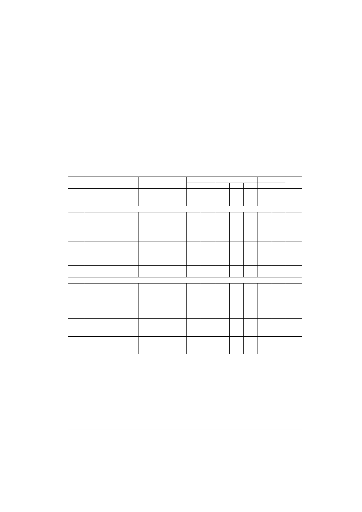
Absolute Maximum Ratings
(Note 1)
(Note 2)
Recommended Operating
Conditions
(Note 2)
Note 1: “Absolute Maximum Ratings” are those values beyond which the
safety of the device can not be guaranteed. Th ey are not meant to imp ly
that the devices should be operated at these lim its. The tab les of “Recom-
mended Operating Conditions” and “Electrical Characteristics” provide conditions for actual dev ic e operation.
Note 2: V
SS
= 0V unless otherwise specified.
DC Electrical Characteristics (Note 2)
Supply Voltage (V
DD
) −0.5V to +18V
Input Voltage (V
IN
) −0.5V to V
CC
+0.5V
Storage Temperature Range (T
S
) −65°C to +150°C
Power Dissipation (P
D
)
Dual-In-Line 700 mW
Small Outline 500 mW
Lead Temperature (T
L
)
(Soldering, 10 seconds) 300
°C
Supply Voltage (V
DD
) 3V to 15V
Input Voltage (V
IN
) 0V to V
DD
Operating Temperature Range (TA) −40°C to +85°C
Symbol Parameter Conditions
−40°C +25°C +85°C
Units
Min Max Min Typ Max Min Max
I
DD
Quiescent Device Current VDD = 5V 1.0 0.01 1.0 7.5 µA
VDD = 10V 2.0 0.01 2.0 15 µA
VDD = 15V 4.0 0.01 4.0 30 µA
SIGNAL INPUTS AND OUTPUTS
R
ON
“ON” Resistance RL = 10 kΩ to (VDD − VSS/2)
VC = VDD, VSS to V
DD
VDD = 5V 850 270 1050 1200 Ω
VDD = 10V 330 120 400 520 Ω
VDD = 15V 210 80 240 300 Ω
∆RON∆“ON” Resistance Between RL = 10 kΩ to (VDD − VSS/2)
Any 2 of 4 Switches VCC = V
DD
, VIS = VSS to V
DD
VDD = 10V 10 Ω
V
DD
= 15V 5 Ω
I
IS
Input or Output Leakage VC = 0 ±50 ±0.1 ±50 ±200 nA
Switch “OFF”
CONTROL INPUTS
V
ILC
LOW Level Input VIS = V
SS
and V
DD
Voltage VOS = V
DD
and V
SS
IIS = ± 10µA
V
DD
= 5V 1.5 2.25 1.5 1.5 V
VDD = 10V 3.0 4.5 3.0 3.0 V
V
DD
= 15V 4.0 6.75 4.0 4.0 V
V
IHC
HIGH Level Input VDD = 5V 3.5 3.5 2.75 3.5 V
Voltage VDD = 10V (Note 7) 7.0 7.0 5.5 7.0 V
VDD = 15V 11.0 11.0 8.25 11.0 V
I
IN
Input Current VDD−V
SS
= 15V ± 0.3 ± 10−5± 0.3 ± 1.0 µA
VDD≥VIS≥V
SS
VDD≥VC≥V
SS
3 www.fairchildsemi.com
CD4066BC
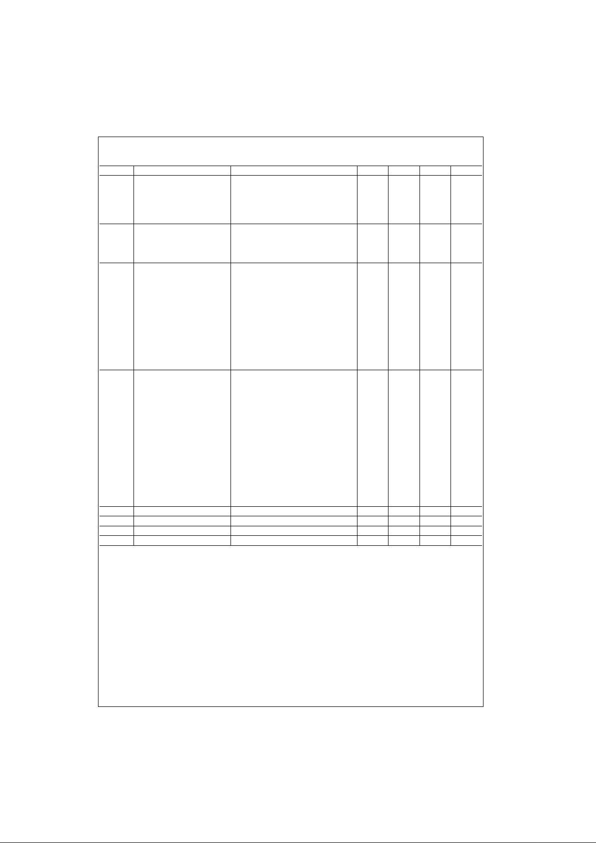
AC Electrical Characteristics (Note 3)
T
A
= 25°C, tr = tf = 20 ns and V
SS
= 0V unless otherwise noted
Note 3: AC Parameters are guar ant eed by DC correlated te s tin g.
Note 4: These devices should not be connected to circuits with the power “ON”.
Note 5: In all cases, there is approx im at ely 5 pF of probe and jig cap ac it ance in the output; howe v er, this capacitance is included in C
L
wherever it is
specified.
Note 6: V
IS
is the voltage at the in/out pin and VOS is the voltage at the out/in pin. VC is the voltage at the cont rol input.
Note 7: Conditions for V
IHC
: a) VIS = VDD, IOS = standard B series IOHb) VIS = 0V, IOL = standard B series IOL.
Symbol Parameter Conditions Min Typ Max Units
t
PHL
, t
PLH
Propagation Delay Time Signal VC = VDD, CL = 50 pF, (Figure 1)
Input to Signal Output RL = 200k
V
DD
= 5V 25 55 ns
V
DD
= 10V 15 35 ns
VDD = 15V 10 25 ns
t
PZH
, t
PZL
Propagation Delay Time RL = 1.0 kΩ, CL = 50 pF, (Figure 2, Figure 3)
Control Input to Signal V
DD
= 5V 125 ns
Output High Impedance to VDD = 10V 60 ns
Logical Level V
DD
= 15V 50 ns
t
PHZ
, t
PLZ
Propagation Delay Time RL = 1.0 kΩ, CL = 50 pF, (Figure 2, Figure 3)
Control Input to Signal VDD = 5V 125 ns
Output Logical Level to V
DD
= 10V 60 ns
High Impedance V
DD
= 15V 50 ns
Sine Wave Distortion VC = VDD = 5V, VSS = −5V 0.1 %
RL = 10 kΩ, VIS = 5V
p-p
, f= 1 kHz, (Figure 4)
Frequency Response-Switch VC = VDD = 5V, VSS = −5V, 40 MHz
“ON” (Frequency at −3 dB) RL = 1 kΩ, VIS = 5V
p-p
,
20 Log10 VOS/VOS (1 kHz)−dB,
(Figure 4)
Feedthrough — Switch “OFF” VDD = 5.0V, VCC = VSS = −5.0V, 1.25
(Frequency at −50 dB) RL = 1 kΩ, VIS = 5.0V
p-p
, 20 Log10,
VOS/VIS = −50 dB, (Figure 4)
Crosstalk Between Any Two VDD = V
C(A)
= 5.0V; VSS = V
C(B)
= 5.0V, 0.9 MHz
Switches (Frequency at −50 dB) R
L
1 kΩ, V
IS(A)
= 5.0 V
p-p
, 20 Log10,
V
OS(B)/VIS(A)
= −50 dB (Figure 5)
Crosstalk; Control Input to VDD = 10V, RL = 10 kΩ, RIN = 1.0 kΩ, 150 mV
p-p
Signal Output VCC = 10V Square Wave, CL = 50 pF
(Figure 6)
Maximum Control Input R
L
= 1.0 kΩ, CL = 50 pF, (Figure 7)
V
OS(f)
= ½ VOS(1.0 kHz)
V
DD
= 5.0V 6.0 MHz
VDD = 10V 8.0 MHz
V
DD
= 15V 8.5 MHz
C
IS
Signal Input Capacitance 8.0 pF
C
OS
Signal Output Capacitance VDD = 10V 8.0 pF
C
IOS
Feedthrough Capacitance VC = 0V 0.5 pF
C
IN
Control Input Capacitance 5.0 7.5 pF

www.fairchildsemi.com 4
CD4066BC
Typical Performance Characteristics
“ON” Resistance vs Signal
Voltage for T
A
= 25°C
“ON” Resistance as a Function
of Temperature for
V
DD−VSS
= 15V
“ON” Resistance as a Function
of Temperature for
V
DD−VSS
= 10V
“ON” Resistance as a Function
of Temperature for
V
DD−VSS
= 5V
Special Considerations
In applications whe re separa te pow er sources are used to
drive V
DD
and the signal inpu t, the VDD current capability
should exceed V
DD/RL
(RL = effective external load of the 4
CD4066BC bilateral switches). This provision avoids any
permanent current flow or clamp action of the V
DD
supply
when power is applied or removed from CD4066BC.
In certain applications, the external load-resistor current
may include both V
DD
and signal-line components. To
avoid drawing V
DD
current when switch curr ent flows into
terminals 1, 4, 8 or 11, the voltage drop across the bidirectional switch must not exceed 0.6V at T
A
≤ 25°C, or 0.4V at
T
A
> 25°C (calculated from RON values shown).
No V
DD
current will flow through RL if the switch current
flows into terminals 2, 3, 9 or 10.

5 www.fairchildsemi.com
CD4066BC
AC Test Circuits and Switching Time Waveforms
FIGURE 1. t
PHL
, t
PLH
Propagation Delay Time Signal Input to Signal Output
FIGURE 2. t
PZH
, t
PHZ
Propagation Delay Time Control to Signal Output
FIGURE 3. t
PZL
, t
PLZ
Propagation Delay Time Control to Signal Output
VC = VDD for distortion and frequency response tests
V
C
= VSS for feedthrough test
FIGURE 4. Sine Wave Distortion, Frequency Response and Feedthrough

www.fairchildsemi.com 6
CD4066BC
AC Test Circuits and Switching Time Waveforms (Continued)
FIGURE 5. Crosstalk Between Any Two Switches
FIGURE 6. Crosstalk: Control Input to Signal Output
FIGURE 7. Maximum Control Input Frequency

7 www.fairchildsemi.com
CD4066BC
Physical Dimensions inches (millimeters) unless otherwise noted
14-Lead Small Outline Integrated Circuit (SOIC), JEDEC MS-120, 0.150 Narrow
Package Number M14A

www.fairchildsemi.com 8
CD4066BC
Physical Dimensions inches (millimeters) unless otherwise noted (Continued)
14-Lead Small Outline Package (SOP), EIAJ TYPE II, 5.3mm Wide
Package Number M14D

9 www.fairchildsemi.com
CD4066BC Quad Bilateral Switch
Physical Dimensions inches (millimeters) unless otherwise noted (Continued)
14-Lead Plastic Dual-In-Line Package (PDIP), JEDEC MS-001, 0.300 Wide
Package Number N14A
Fairchild does not assume any responsibility for use of any circuitry described , no circuit patent licenses are implied and
Fairchild reserves the right at any time without notice to change said circuitry and specifications.
LIFE SUPPORT POLICY
FAIRCHILD’S PRODUCTS ARE NOT AUTHORIZED FOR USE AS CRITICAL COMPONENTS IN LIFE SUPPORT
DEVICES OR SYSTEMS WITHOUT THE EXPRESS WRITTEN APPROVAL OF THE PRESIDENT OF FAIRCHILD
SEMICONDUCTOR CORPORATION. As used herein:
1. Life support devices or systems are dev ic es or syste ms
which, (a) are intended for surgical implant into the
body, or (b) support or sustain life, and (c) whose failure
to perform when properly used in accordance with
instructions for use provide d in the labe l ing, can be re asonably expected to result in a significant injury to the
user.
2. A critical compo nent in any com ponen t of a life s upp ort
device or system whose failure to perform can be reasonably expected to cause the failure of the l ife support
device or system, or to affect its safety or effectiveness.
www.fairchildsemi.com
 Loading...