

CD4050BMS
December 1992 File Number 3193
CMOS Hex Buffer/Converter
The CD4050BMS is an non-inverting hex buffer and features
logic level conversion using only one supply voltage (VCC).
The input signal high level (VIH) can exceed the VCC supply
voltage when this device is used for logic level conversions.
This device is intended for use as CMOS to DTL/TTL
converters and can drive directly two DTL/TTL loads. (VCC
= 5V, VOL ≤ 0.4V, and IOL ≥ 3.3mA.
The CD4050BMS is designated as replacement for
CD4010B. Because the CD4050BMS requires only one
power supply, it is preferred over the CD4010B and should
be used in place of the CD4010B in all inverter, current
driver, or logic level conversion applications. In these applications the CD4050BMS is pin compatible with the
CD4010B, and can be substituted for this device in existing
as well as in new designs. Terminal No. 16 is not connected
internally on the CD4050BMS, therefore, connection to this
terminal is of no consequence to circuit operation. For applications not requiring high sink current or voltage conversion,
the CD4069UB Hex Inverter is recommended.
The CD4050BMS is supplied in these 16 lead outline packages:
Braze Seal DIP H4T
Frit Seal DIP H1E
Ceramic Flatpack H3X
Features
• High Voltage Type (20V Rating)
• Non-Inverting Type
• High Sink Current for Driving 2 TTL Loads
• High-to-Low Level Logic Conversion
• 100% Tested for Quiescent Current at 20V
• Maximum Input Current of 1µA at 18V Over Full Pack-
age Temperature Range; 100nA at 18V and +25
o
C
• 5V, 10V and 15V Parametric Ratings
Applications
• CMOS to DTL/TTL Hex Converter
• CMOS Current “Sink” or “Source” Driver
• CMOS High-to-Low Logic Level Converter
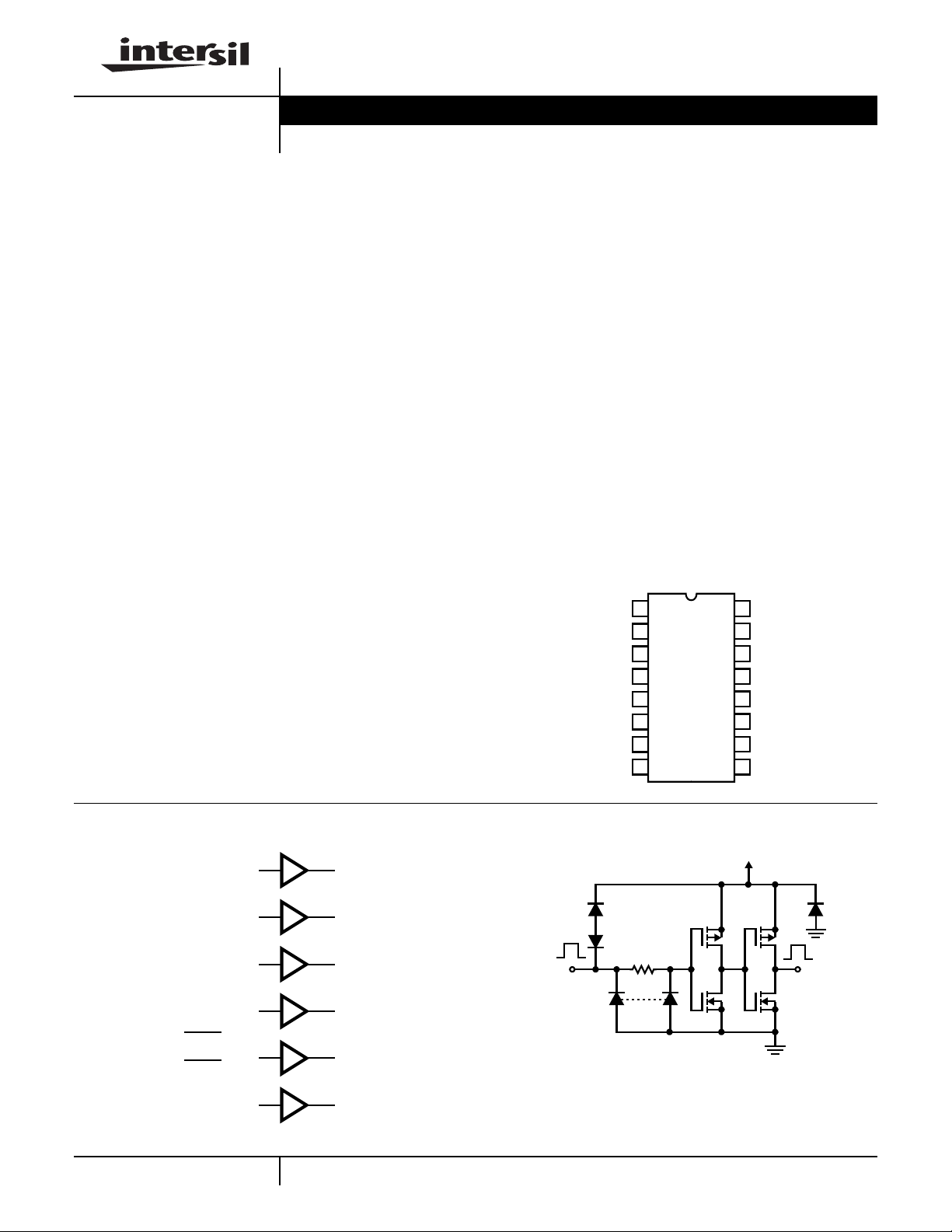
Pinout
VCC
G = A
H = B
I = C
VSS
1
2
3
A
4
B
5
6
C
7
8
CD4050BMS
TOP VIEW
NC
16
L = F
15
F
14
NC
13
K = E
12
E
11
J = D
10
D
9
Functional Diagram Schematic Diagram
32
A G = A
54
B H = B
VCC
VSS
NC = 13
NC = 16
C I = C
D J = D
1
8
E K = E
F L = F
4-1
76
910
11 12
14 15
IN
FIGURE 1. SCHEMATIC DIAGRAM, 1 OF 6 IDENTICAL UNITS
CAUTION: These devices are sensitive to electrostatic discharge; follow proper IC Handling Procedures.
www.intersil.com or 407-727-9207
R
VCC
P
N
| Copyright © Intersil Corporation 1999
P
OUT
N
VSS
CD4050BMS
Absolute Maximum Ratings Reliability Information
DC Supply Voltage Range, (VDD) . . . . . . . . . . . . . . . .-0.5V to +20V
(Voltage Referenced to VSS Terminals)
Input Voltage Range, All Inputs . . . . . . . . . . . . . -0.5V to VDD +0.5V
DC Input Current, Any One Input. . . . . . . . . . . . . . . . . . . . . . . . .±10mA
Operating Temperature Range . . . . . . . . . . . . . . . -55oC to +125oC
Package Types D, F, K, H
Storage Temperature Range (TSTG). . . . . . . . . . . -65oC to +150oC
Lead Temperature (During Soldering) . . . . . . . . . . . . . . . . . +265oC
At Distance 1/16 ± 1/32 Inch (1.59mm ± 0.79mm) from case for
10s Maximum
TABLE 1. DC ELECTRICAL PERFORMANCE CHARACTERISTICS
PARAMETER SYMBOL CONDITIONS (NOTE 1)
Supply Current IDD VDD = 20V, VIN = VDD or GND 1 +25
VDD = 18V, VIN = VDD or GND 3 -55
Input Leakage Current IIL VIN = VDD or GND VDD = 20 1 +25
VDD = 18V 3 -55
Input Leakage Current IIH VIN = VDD or GND VDD = 20 1 +25
VDD = 18V 3 -55
Output Voltage VOL15 VDD = 15V, No Load 1, 2, 3 +25
Output Voltage VOH15 VDD = 15V, No Load (Note 3) 1, 2, 3 +25
Output Current (Sink) IOL4 VDD = 4.5V, VOUT = 0.4V 1 +25
Output Current (Sink) IOL5 VDD = 5V, VOUT = 0.4V 1 +25
Output Current (Sink) IOL10 VDD = 10V, VOUT = 0.5V 1 +25
Output Current (Sink) IOL15 VDD = 15V, VOUT = 1.5V 1 +25
Output Current (Source) IOH5A VDD = 5V, VOUT = 4.6V 1 +25
Output Current (Source) IOH5B VDD = 5V, VOUT = 2.5V 1 +25
Output Current (Source) IOH10 VDD = 10V, VOUT = 9.5V 1 +25
Output Current (Source) IOH15 VDD = 15V, VOUT = 13.5V 1 +25
N Threshold Voltage VNTH VDD = 10V, ISS = -10µA 1 +25
P Threshold Voltage VPTH VSS = 0V, IDD = 10µA 1 +25
Functional F VDD = 2.8V, VIN = VDD or GND 7 +25
VDD = 20V, VIN = VDD or GND 7 +25
VDD = 18V, VIN = VDD or GND 8A +125
VDD = 3V, VIN = VDD or GND 8B -55
Input Voltage Low
VIL VDD = 5V, VOH > 4.5V, VOL < 0.5V 1, 2, 3 +25
(Note 2)
Input Voltage High
VIH VDD = 5V, VOH > 4.5V, VOL < 0.5V 1, 2, 3 +25
(Note 2)
Input Voltage Low
(Note 2)
Input Voltage High
(Note 2)
VIL VDD = 15V, VOH > 13.5V,
VOL < 1.5V
VIH VDD = 15V, VOH > 13.5V,
VOL < 1.5V
NOTES: 1. All voltages referenced to device GND, 100% testing being im-
plemented.
2. Go/No Go test with limits applied to inputs.
Thermal Resistance. . . . . . . . . . . . . . . . θ
Ceramic DIP and FRIT Package . . . . 80oC/W 20oC/W
Flatpack Package. . . . . . . . . . . . . . . . 70oC/W 20oC/W
Maximum Package Power Dissipation (PD) at +125oC
For TA = -55oC to +100oC (Package Type D, F, K) . . . . . .500mW
For TA = +100oC to +125oC (Package Type D, F, K) . . . . . Derate
Device Dissipation per Output Transistor. . . . . . . . . . . . . . . .100mW
For TA = Full Package Temperature Range (All Package Types)
Junction Temperature . . . . . . . . . . . . . . . . . . . . . . . . . . . . . .+175oC
GROUP A
SUBGROUPS TEMPERATURE
2 +125
2 +125
2 +125
o
C, +125oC, -55oC - 50 mV
o
C, +125oC, -55oC 14.95 - V
o
C, +125oC, -55oC - 1.5 V
o
C, +125oC, -55oC 3.5 - V
o
1, 2, 3 +25
1, 2, 3 +25
C, +125oC, -55oC- 4 V
o
C, +125oC, -55oC11 - V
3. For accuracy,voltage ismeasured differentiallyto VDD.Limit is
0.050V max.
ja
θ
jc
Linearity at 12mW/oC to 200mW
LIMITS
UNITSMIN MAX
o
C-2µA
o
C - 200 µA
o
C-2µA
o
C -100 - nA
o
C -1000 - nA
o
C -100 - nA
o
C - 100 nA
o
C - 1000 nA
o
C - 100 nA
o
C 2.6 - mA
o
C 3.2 - mA
o
C 8.0 - mA
o
C24-mA
o
C - -0.8 mA
o
C - -3.2 mA
o
C - -1.8 mA
o
C - -6.0 mA
o
C -2.8 -0.7 V
o
C 0.7 2.8 V
o
C VOH >
o
C
o
C
o
C
VDD/2
VOL <
VDD/2
V
4-2
CD4050BMS
TABLE 2. AC ELECTRICAL PERFORMANCE CHARACTERISTICS
GROUP A
PARAMETER SYMBOL CONDITIONS (NOTE 1, 2)
Propagation Delay TPHL VDD = 5V, VIN = VDD or GND 9 +25
Propagation Delay TPLH VDD = 5V, VIN = VDD or GND 9 +25oC - 140 ns
Transition Time TTHL VDD = 5V, VIN = VDD or GND 9 +25oC - 60 ns
Transition Time TTLH VDD = 5V, VIN = VDD or GND 9 +25oC - 160 ns
NOTES:
1. CL = 50pF, RL = 200K, Input TR, TF < 20ns.
2. -55oC and +125oC limits guaranteed, 100% testing being implemented.
TABLE 3. ELECTRICAL PERFORMANCE CHARACTERISTICS
PARAMETER SYMBOL CONDITIONS NOTES TEMPERATURE
Supply Current IDD VDD = 5V, VIN = VDD or GND 1, 2 -55
VDD = 10V, VIN = VDD or GND 1, 2 -55oC, +25oC- 2 µA
VDD = 15V, VIN = VDD or GND 1, 2 -55oC, +25oC- 2 µA
Output Voltage VOL VDD = 5V, No Load 1, 2 +25oC, +125oC, -
Output Voltage VOL VDD = 10V, No Load 1, 2 +25oC, +125oC, -
Output Voltage VOH VDD = 5V, No Load 1, 2 +25oC, +125oC, -
Output Voltage VOH VDD = 10V, No Load 1, 2 +25oC, +125oC, -
Output Current (Sink) IOL4 VDD = 4.5V, VOUT = 0.4V 1, 2 +125oC 1.8 - mA
Output Current (Sink) IOL5 VDD = 5V, VOUT = 0.4V 1, 2 +125oC 2.4 - mA
Output Current (Sink) IOL10 VDD = 10V, VOUT = 0.5V 1, 2 +125oC 5.6 - mA
Output Current (Sink) IOL15 VDD = 15V, VOUT = 1.5V 1, 2 +125oC18-mA
Output Current (Source) IOH5A VDD = 5V, VOUT = 4.6V 1, 2 +125oC - -0.48 mA
Output Current (Source) IOH5B VDD = 5V, VOUT = 2.5V 1, 2 +125oC - -1.55 mA
Output Current (Source) IOH10 VDD = 10V, VOUT = 9.5V 1, 2 +125oC - -1.18 mA
Output Current (Source) IOH15 VDD =15V, VOUT = 13.5V 1, 2 +125oC - -3.1 mA
SUBGROUPS TEMPERATURE
o
C - 110 ns
10, 11 +125oC, -55oC - 149 ns
10, 11 +125oC, -55oC - 189 ns
10, 11 +125oC, -55oC - 81 ns
10, 11 +125oC, -55oC - 216 ns
o
C, +25oC- 1 µA
+125oC-30µA
+125oC-60µA
+125oC - 120 µA
55oC
55oC
55oC
55oC
-55oC 3.3 - mA
-55oC 4.0 - mA
-55oC10-mA
-55oC26-mA
-55oC - -0.81 mA
-55oC - -2.6 mA
-55oC - -2.0 mA
-55oC - -5.2 mA
LIMITS
UNITSMIN MAX
LIMITS
UNITSMIN MAX
-50mV
-50mV
4.95 - V
9.95 - V
4-3

CD4050BMS
TABLE 3. ELECTRICAL PERFORMANCE CHARACTERISTICS (Continued)
LIMITS
PARAMETER SYMBOL CONDITIONS NOTES TEMPERATURE
Input Voltage Low VIL VDD = 10V, VOH > 9V, VOL < 1V 1, 2 +25oC, +125oC, -
-3V
55oC
Input Voltage High VIH VDD = 10V, VOH > 9V, VOL < 1V 1, 2 +25oC, +125oC, -
+7 - V
55oC
Propagation Delay TPHL VIN = 10V, VDD = 5V 1, 2, 3 +25oC - 100 ns
VIN = 10V, VDD = 10V 1, 2, 3 +25oC - 55 ns
Propagation Delay TPLH VIN = 10V, VDD = 5V 1, 2, 3 +25oC - 90 ns
VIN = 10V, VDD = 10V 1, 2, 3 +25oC - 80 ns
Propagation Delay TPHL VIN = 15V, VDD = 5V 1, 2, 3 +25oC - 100 ns
VIN = 15V, VDD = 15V 1, 2, 3 +25oC - 30 ns
Propagation Delay TPLH VIN = 15V, VDD = 5V 1, 2, 3 +25oC - 80 ns
VIN = 15V, VDD = 15V 1, 2, 3 +25oC - 60 ns
Transition Time TTHL VDD = 10V, VIN = VDD OR GND 1, 2, 3 +25oC - 40 ns
VDD = 15V, VIN = VDD OR GND 1, 2, 3 +25oC - 30 ns
Transition Time TTLH VDD = 10V, VIN = VDD OR GND 1, 2, 3 +25oC - 80 ns
VDD = 15V, VIN = VDD OR GND 1, 2, 3 +25oC - 60 ns
Input Capacitance CIN Any Input 1, 2 +25oC - 7.5 pF
NOTES:
1. All voltages referenced to device GND.
2. The parameterslisted on Table 3 are controlled via design or process and are not directly tested. These parameters are characterized on initial
design release and upon design changes which would affect these characteristics.
3. CL = 50pF, RL = 200K, Input TR, TF < 20ns.
UNITSMIN MAX
TABLE 4. POST IRRADIATION ELECTRICAL PERFORMANCE CHARACTERISTICS
PARAMETER SYMBOL CONDITIONS NOTES TEMPERATURE
Supply Current IDD VDD = 20V, VIN = VDD or GND 1, 4 +25
N Threshold Voltage VNTH VDD = 10V, ISS = -10µA 1, 4 +25
N Threshold Voltage
∆VTN VDD = 10V, ISS = -10µA 1, 4 +25
Delta
P Threshold Voltage VTP VSS = 0V, IDD = 10µA 1, 4 +25
P Threshold Voltage
∆VTP VSS = 0V, IDD = 10µA 1, 4 +25
Delta
Functional F VDD = 18V, VIN = VDD or GND 1 +25
VDD = 3V, VIN = VDD or GND
Propagation Delay Time TPHL
VDD = 5V 1, 2, 3, 4 +25
TPLH
NOTES: 1. All voltages referenced to device GND.
2. CL = 50pF, RL = 200K, Input TR, TF < 20ns.
3. See Table 2 for +25
4. Read and Record
o
TABLE 5. BURN-IN AND LIFE TEST DELTA PARAMETERS +25OC
PARAMETER SYMBOL DELTA LIMIT
Supply Current - MSI-1 IDD ± 0.2µA
Output Current (Sink) IOL5 ± 20% x Pre-Test Reading
Output Current (Source) IOH5A ± 20% x Pre-Test Reading
LIMITS
UNITSMIN MAX
o
C - 7.5 µA
o
C -2.8 -0.2 V
o
C-±1V
o
C 0.2 2.8 V
o
C-±1V
o
C VOH >
VDD/2
o
C - 1.35 x
VOL <
VDD/2
V
ns
+25oC
Limit
C limit.
4-4

CD4050BMS
TABLE 6. APPLICABLE SUBGROUPS
MIL-STD-883
CONFORMANCE GROUP
Initial Test (Pre Burn-In) 100% 5004 1, 7, 9 IDD, IOL5, IOH5A
Interim Test 1 (Post Burn-In) 100% 5004 1, 7, 9 IDD, IOL5, IOH5A
Interim Test 2 (Post Burn-In) 100% 5004 1, 7, 9 IDD, IOL5, IOH5A
PDA (Note 1) 100% 5004 1, 7, 9, Deltas
Interim Test 3 (Post Burn-In) 100% 5004 1, 7, 9 IDD, IOL5, IOH5A
PDA (Note 1) 100% 5004 1, 7, 9, Deltas
Final Test 100% 5004 2, 3, 8A, 8B, 10, 11
Group A Sample 5005 1, 2, 3, 7, 8A, 8B, 9, 10, 11
Group B Subgroup B-5 Sample 5005 1, 2, 3, 7, 8A, 8B, 9, 10, 11, Deltas Subgroups 1, 2, 3, 9, 10, 11
Subgroup B-6 Sample 5005 1, 7, 9
Group D Sample 5005 1, 2, 3, 8A, 8B, 9 Subgroups 1, 2 3
NOTE: 1. 5% Parametric, 3% Functional; Cumulative for Static 1 and 2.
CONFORMANCE GROUPS
Group E Subgroup 2 5005 1, 7, 9 Table 4 1, 9 Table 4
METHOD GROUP A SUBGROUPS READ AND RECORD
TABLE 7. TOTAL DOSE IRRADIATION
MIL-STD-883
METHOD
PRE-IRRAD POST-IRRAD PRE-IRRAD POST-IRRAD
TEST READ AND RECORD
TABLE 8. BURN-IN AND IRRADIATION TEST CONNECTIONS
OSCILLATOR
FUNCTION OPEN GROUND VDD 9V ± -0.5V
50kHz 25kHz
Static Burn-In 1 (Note 1) 2, 4, 6, 10, 12, 13, 15 3, 5, 7-9, 11-14 1, 16
Static Burn-In 2 (Note 1) 2, 4, 6, 10, 12, 13, 15 8 1, 3, 5, 7, 9, 11, 14, 16
Dynamic Burn-In (Note 3) 13 8 1, 16 2, 4, 6, 10, 12, 15 3, 5, 7, 9, 11, 14
Irradiation (Note 2) 2, 4, 6, 10, 12, 13, 15,16 8 1, 3, 5, 7, 9, 11, 14
NOTES:
1. Each pin except pin 1, pin 16, and GND will have a series resistor of 10K ± 5%, VDD = 18V ± 0.5V
2. Each pin except pin 1, pin 16, and GND will have a series resistor of 47K ±5%; Group E, Subgroup 2, sample size is 4 dice/wafer, 0 failures, VDD
= 10V ± 0.5V
3. Each pin except pin 1, pin 16, and GND will have a series resistor of 4.75K ± 5%, VDD = 10V ± 0.5V
Typical Performance Characteristics
AMBIENT TEMPERATURE (TA) = +25oC
SUPPLY VOLTAGE (VCC) = 5V
5
4
MINIMUM
3
OUTPUT VOLTAGE (VO) (V)
2
1
01234
INPUT VOLTAGE (VI) (V)
MAXIMUM
AMBIENT TEMPERATURE (TA) = +25oC
70
60
50
40
30
20
10
OUTPUT LOW (SINK) CURRENT (IOL) (mA)
0
12345678
DRAIN-TO-SOURCE VOLTAGE (VDS) (V)
10V15V
GATE-TO-SOURCE VOLTAGE (V GS) = 5V
FIGURE 2. MINIMUM AND MAXIMUM VOLTAGE TRANSFER
CHARACTERISTICS
4-5
FIGURE 3. TYPICAL OUTPUT LOW (SINK) CURRENT
CHARACTERISTICS

CD4050BMS
Typical Performance Characteristics
(Continued)
AMBIENT TEMPERATURE (TA) = +25oC
70
60
15V
10V
50
40
30
20
GATE-TO-SOURCE VOLTAGE (V GS) = 5V
10
OUTPUT LOW (SINK) CURRENT (IOL) (mA)
0
12345678
DRAIN-TO-SOURCE VOLTAGE (VDS) (V)
FIGURE 4. MINIMUM OUTPUT LOW (SINK) CURRENT DRAIN
CHARACTERISTICS
DRAIN-TO-SOURCE VOLTAGE (VDS) (V)
0
-1-2-3-4-5-6-7-8
AMBIENT TEMPERATURE (TA) = +25oC
GATE-TO-SOURCE VOLTAGE (V GS) = 5V
-10V
-15V
-5
-10
-15
-20
-25
-30
-35
DRAIN-TO-SOURCE VOLTAGE (VDS) (V)
AMBIENT TEMPERATURE (TA) = +25oC
GATE-TO-SOURCE VOLTAGE (V GS) = 5V
-10V
-15V
FIGURE 5. TYPICAL OUTPUT HIGH (SOURCE) CURRENT
CHARACTERISTICS
SUPPLY VOLTAGE (VCC) = 10V
AMBIENT TEMP (TA)
10
9
8
7
6
5
4
3
OUTPUT VOLTAGE (VO) (V)
2
1
OUTPUT HIGH (SINK) CURRENT (IOH) (mA)
o
C
= -55
+125oC
012345678910
+125oC
VCC = 5V
-55oC
INPUT VOLTAGE (VI) (V)
0
-1-2-3-4-5-6-7-8
-5
-10
-15
-20
-25
-30
-35
OUTPUT HIGH (SINK) CURRENT (IOH) (mA)
FIGURE 6. MINIMUM OUTPUT HIGH (SOURCE) CURRENT
CHARACTERISTICS
5
AMBIENT TEMPERATURE (TA)
POWER DISSIPATION PER INVERTER (µW)
10
4
10
3
10
2
10
10
o
8
6
4
2
8
6
4
2
8
6
4
2
8
6
4
2
C
= +25
SUPPLY VOLTAGE
(VDD) = 15V
10
10V
10V
5V
LOAD CAPACITANCE (CL) = 50pF
(11pF FIXTURE + 39pF EXT)
CL = 15pF (11pF FIXTURE + 4pF EXT
864286422
2
10
3
10
864
4
10
2864
INPUT FREQUENCY (f) (kHz)
FIGURE 8. TYPICAL POWER DISSIPATION vs FREQUENCY
CHARACTERISTICS
4-6
FIGURE 7. TYPICAL VOLTAGE TRANSFER CHARACTERIS-
TICS AS A FUNCTION OF TEMPERATURE
6
10
AMBIENT TEMPERATURE (TA) = +25oC
5
10
4
10
15V; 1MHz
15V; 100KHz
3
10
2
10
10
SUPPLY VOLTAGE (VCC) = 5V
1
POWER DISSIPATION PER INVERTER (PD) (µW)
5
10
10
FREQUENCY (f) = 10KHz
2
10310410
10
INPUT RISE AND FALL TIME (tr, tf) (ns)
10V; 10KHz
15V; 1KHz
10V; 100KHz
15V; 10KHz
5
10610710
8
FIGURE 9. TYPICAL POWER DISSIPATION vs INPUT RISE
AND FALL TIMES PER INVERTER

Chip Dimensions and Pad Layout
CD4050BMS
Dimensions in parenthesis are in millimeters and are derived
from the basic inch dimensions as indicated. Grid
graduations are in mils (10
-3
inch).
METALLIZATION: Thickness: 11kÅ − 14kÅ, AL.
PASSIVATION: 10.4kÅ - 15.6kÅ, Silane
BOND PADS: 0.004 inches X 0.004 inches MIN
DIE THICKNESS: 0.0198 inches - 0.0218 inches
All Intersil semiconductor products are manufactured, assembled and tested under ISO9000 quality systems certification.
Intersil semiconductor products are sold by description only. Intersil Corporation reserves the right to make changes in circuit design and/or specifications at any time without notice. Accordingly, the reader is cautioned to verify that data sheets are current before placing orders. Information furnished by Intersil is believed to be accurate and
reliable. However ,no responsibility is assumed by Intersil or its subsidiaries for its use; nor for any infringements of patents or other rights of third parties which may result
from its use. No license is granted by implication or otherwise under any patent or patent rights of Intersil or its subsidiaries.
For information regarding Intersil Corporation and its products, see web site http://www.intersil.com
Sales Office Headquarters
NORTH AMERICA
Intersil Corporation
P. O. Box 883, Mail Stop 53-204
Melbourne, FL 32902
TEL: (407) 724-7000
FAX: (407) 724-7240
EUROPE
Intersil SA
Mercure Center
100, Rue de la Fusee
1130 Brussels, Belgium
TEL: (32) 2.724.2111
FAX: (32) 2.724.22.05
ASIA
Intersil (Taiwan) Ltd.
7F-6, No. 101 Fu Hsing North Road
Taipei, Taiwan
Republic of China
TEL: (886) 2 2716 9310
FAX: (886) 2 2715 3029
4-7
 Loading...