

Page 1
December 1992
CD4034BMS
CMOS 8-Stage Static Bidirectional Parallel/Serial
Input/Output Bus Register
Features
• High Voltage Types (20V Rating)
• Bidirectional Parallel Data Input
• Parallel or Serial Inputs/Parallel Outputs
• Asynchronous or Synchronous Parallel Data Loading
• Parallel Data-Input Enable on “A” Data Lines (3-State
Output)
• Data Recirculation for Register Expansion
• Multipackage Register Expansion
• Fully Static Operation DC-to-10MHz (typ.) at
VDD = 10V
• Standardized Symmetrical Output Characteristics
• 100% Tested for Quiescent Current at 20V
• 5V, 10V and 15V Parametric Ratings
• Maximum Input Current of 1µA at 18V Over Full
Package-Temperature Range;
o
- 100nA at 18V and +25
C
• Noise Margin (Over Full Package T emperature Range):
- 1V at VDD = 5V
- 2V at VDD = 10V
- 2.5V at VDD = 15V
• Meets All Requirements of JEDEC Tentative Standard
No. 13B, “Standard Specifications for Description of
‘B’ Series CMOS Devices”
Applications
• Parallel Input/Parallel Output, Serial Input/Parallel Output, Serial Input/Serial Output Register
• Shift Right/Shift Left Register
• Shift Right/Shift Left With Parallel Loading
• Address Register
• Buffer Register
• Bus System Register with Enable Parallel Lines at Bus
Side
• Double Bus Register System
• Up-Down Johnson or Ring Counter
• Pseudo-Random Code Generators
• Sample and Hold Register (Storage, Counting,
Display)
• Frequency and Phase Comparator
Description
CD4034BMS is a static eight-stage parallel-or serial-input
parallel-output register. It can be used to:
1) bidirectionally transfer parallel information between two
buses, 2) convert serial data to parallel form and direct the
parallel data to either of two buses, 3) store (recirculate) parallel data, or 4) accept parallel data from either of two buses
and convert that data to serial form. Inputs that control the
operations include a single-phase CLOCK (CL), A DATA
ENABLE (AE), ASYNCHRONOUS/SYNCHRONOUS (A/S),
A-BUS-TO-B-BUS/B-BUS-TO-A-BUS (A/B), and PARALLEL/SERIAL (P/S).
Data inputs include 16 bidirectional parallel data lines of
which the eight A data lines are inputs (3-state outputs) and
the B data lines are outputs (inputs) depending on the signal
level on the A/B input. In addition, an input for SERIAL DATA
is also provided.
All register stages are D-type master-slave flip-flops with
separate master and slave clock inputs generated internally
to allow synchronous or asynchronous data transfer from
master to slave. Isolation from external noise and the effects
of loading is provided by output buffering.
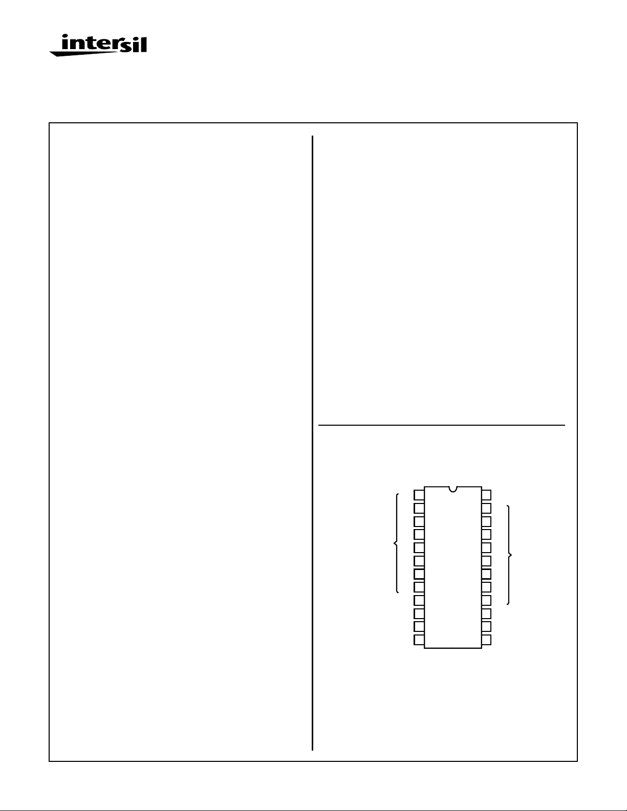
Pinout
CD4034BMS
TOP VIEW
24
23
22
21
20
19
18
17
16
15
14
13
VDD
8
7
6
5
4
3
2
1
CLOCK
A/S
P/S
“A” DATA LINES
“B” DATA LINES
“A” ENABLE
SERIAL INPUT
A/B
VSS
1
8
2
7
3
6
4
5
5
4
6
3
7
2
8
1
9
10
11
12
CAUTION: These devices are sensitive to electrostatic discharge; follow proper IC Handling Procedures.
1-888-INTERSIL or 321-724-7143 | Copyright © Intersil Corporation 1999
7-837
File Number
3307
Page 2
CD4034BMS
Parallel Operation
A high P/S input signal allows data transfer into the register
via the parallel data lines synchronously with the positive
transition of the clock provided the A/S input is low. If the A/S
input is high the transfer is independent of the clock. The
direction of data flow is controlled by the A/B input. When
this signal is high the A data lines are inputs (and B data
lines are outputs); a low A/B signal reverses the direction of
data flow.
The AE input is an additional feature which allows many registers to feed data to a common bus. The A DATA lines are
enabled only when this signal is high.
Data storage through recirculation of data in each register
stage is accomplished by making the A/B signal high and the
AE signal low.
Serial Operation
A low P/S signal allows serial data to transfer into the register synchronously with the positive transition of the clock.
The A/S input is internally disabled when the register is in
the serial mode (asynchronous serial operation is not
allowed).
The serial data appears as output data on either the B lines
(when A/B is high) or the A lines (when A/B is low and the
AE signal is high).
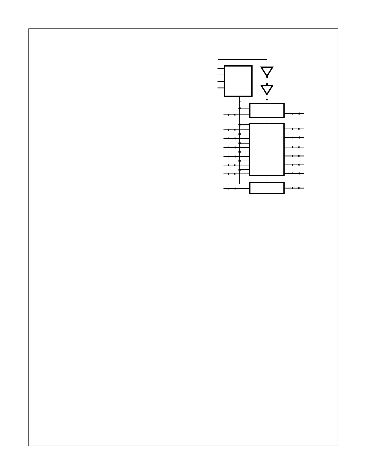
Functional Diagram
SI
AE
A/B
A/S
P/S
CL
STEERING
A DATA LINES
LOGIC
SI
A1 B1Q
SI
6
STAGES
Q
SI
A8 B8
B DATA LINES
Register expansion can be accomplished by simply cascading CD4034BMS packages.
The CD4034BMS is supplied in these 24 lead outline packages:
Braze Seal DIP H4V
Ceramic Flatpack H4P
7-838
Page 3
Specifications CD4034BMS
Absolute Maximum Ratings Reliability Information
DC Supply Voltage Range, (VDD) . . . . . . . . . . . . . . . -0.5V to +20V
(Voltage Referenced to VSS Terminals)
Input Voltage Range, All Inputs . . . . . . . . . . . . .-0.5V to VDD +0.5V
DC Input Current, Any One Input . . . . . . . . . . . . . . . . . . . . . . . .±10mA
Operating Temperature Range. . . . . . . . . . . . . . . . -55
Package Types D, F, K, H
Storage Temperature Range (TSTG) . . . . . . . . . . . -65
o
C to +125oC
o
C to +150oC
Lead Temperature (During Soldering) . . . . . . . . . . . . . . . . . +265
At Distance 1/16 ± 1/32 Inch (1.59mm ± 0.79mm) from case for
10s Maximum
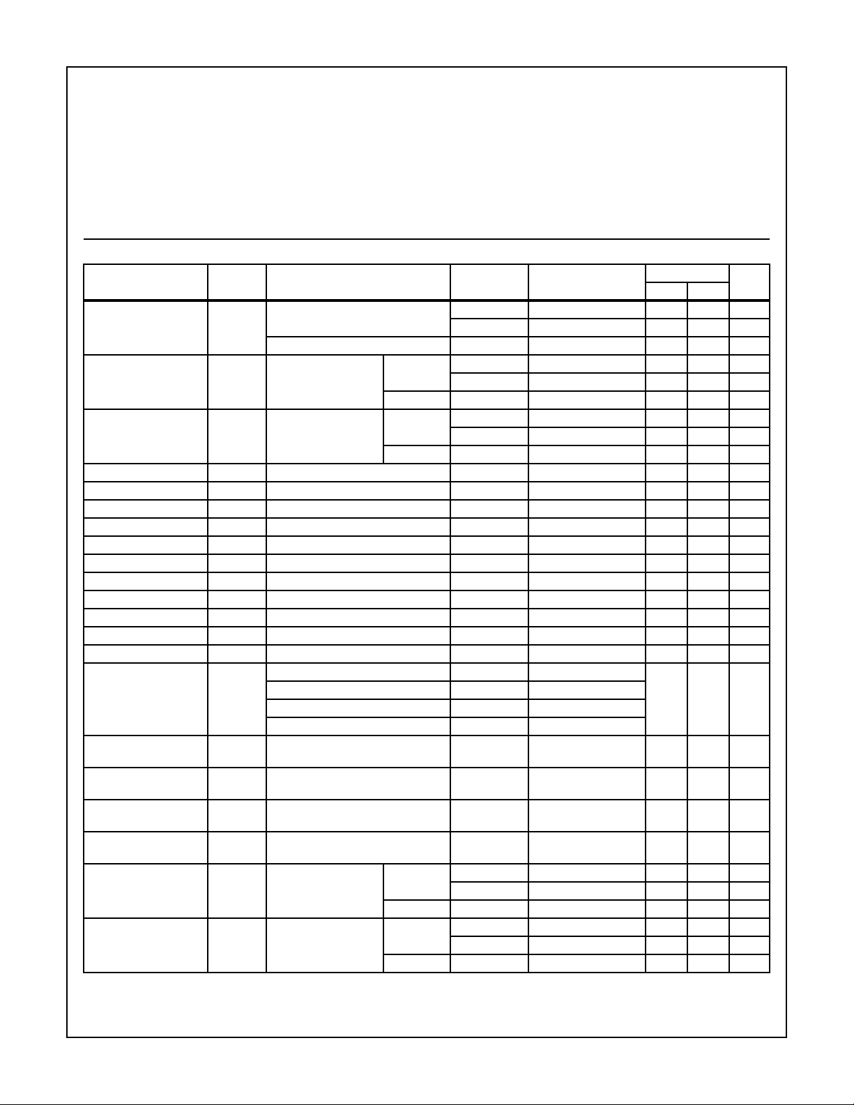
TABLE 1. DC ELECTRICAL PERFORMANCE CHARACTERISTICS
PARAMETER SYMBOL CONDITIONS (NOTE 1)
Supply Current IDD VDD = 20V, VIN = VDD or GND 1 +25oC-10µA
VDD = 18V, VIN = VDD or GND 3 -55
Input Leakage Current
IIL VIN = VDD or GND VDD = 20 1 +25
Except A and B Lines
VDD = 18V 3 -55oC -100 - nA
Input Leakage Current
IIH VIN = VDD or GND VDD = 20 1 +25oC - 100 nA
Except A and B Lines
VDD = 18V 3 -55oC - 100 nA
Output Voltage VOL15 VDD = 15V, No Load 1, 2, 3 +25oC, +125oC, -55oC - 50 mV
Output Voltage VOH15 VDD = 15V, No Load (Note 3) 1, 2, 3 +25oC, +125oC, -55oC 14.95 - V
Output Current (Sink) IOL5 VDD = 5V, VOUT = 0.4V 1 +25oC 0.53 - mA
Output Current (Sink) IOL10 VDD = 10V, VOUT = 0.5V 1 +25oC 1.4 - mA
Output Current (Sink) IOL15 VDD = 15V, VOUT = 1.5V 1 +25oC 3.5 - mA
Output Current (Source) IOH5A VDD = 5V, VOUT = 4.6V 1 +25oC - -0.53 mA
Output Current (Source) IOH5B VDD = 5V, VOUT = 2.5V 1 +25oC - -1.8 mA
Output Current (Source) IOH10 VDD = 10V, VOUT = 9.5V 1 +25oC - -1.4 mA
Output Current (Source) IOH15 VDD = 15V, VOUT = 13.5V 1 +25oC - -3.5 mA
N Threshold Voltage VNTH VDD = 10V, ISS = -10µA 1 +25oC -2.8 -0.7 V
P Threshold Voltage VPTH VSS = 0V, IDD = 10µA 1 +25oC 0.7 2.8 V
Functional F VDD = 2.8V, VIN = VDD or GND 7 +25oC VOH >
VDD = 20V, VIN = VDD or GND 7 +25oC
VDD = 18V, VIN = VDD or GND 8A +125oC
VDD = 3V, VIN = VDD or GND 8B -55oC
Input Voltage Low
VIL VDD = 5V, VOH > 4.5V, VOL < 0.5V 1, 2, 3 +25oC, +125oC, -55oC - 1.5 V
(Note 2)
Input Voltage High
VIH VDD = 5V, VOH > 4.5V, VOL < 0.5V 1, 2, 3 +25oC, +125oC, -55oC 3.5 - V
(Note 2)
Input Voltage Low
(Note 2)
Input Voltage High
(Note 2)
Tri-State Output
Leakage
VIL VDD = 15V, VOH > 13.5V,
VOL < 1.5V
VIH VDD = 15V, VOH > 13.5V,
VOL < 1.5V
IOZL VIN = VDD or GND
VOUT = 0V
VDD = 20V 1 +25oC -0.4 - µA
VDD = 18V 3 -55oC -0.4 - µA
Tri-State Output
Leakage
IOZH VIN = VDD or GND
VOUT = VDD
VDD = 20V 1 +25oC - 0.4 µA
VDD = 18V 3 -55oC - 0.4 µA
NOTES: 1. All voltages referenced to device GND, 100% testing being
implemented.
2. Go/No Go test with limits applied to inputs.
Thermal Resistance . . . . . . . . . . . . . . . . θ
Ceramic DIP and FRIT Package. . . . . 80oC/W 20oC/W
Flatpack Package . . . . . . . . . . . . . . . . 70
Maximum Package Power Dissipation (PD) at +125oC
For TA = -55
For TA = +100
o
C
Device Dissipation per Output Transistor . . . . . . . . . . . . . . . 100mW
o
C to +100oC (Package Type D, F, K). . . . . . 500mW
o
C to +125oC (Package Type D, F, K) . . . . .Derate
Linearity at 12mW/oC to 200mW
ja
o
C/W 20oC/W
For TA = Full Package Temperature Range (All Package Types)
Junction Temperature . . . . . . . . . . . . . . . . . . . . . . . . . . . . . . +175oC
GROUP A
LIMITS
SUBGROUPS TEMPERATURE
2 +125oC - 1000 µA
o
C-10µA
o
C -100 - nA
2 +125oC -1000 - nA
2 +125oC - 1000 nA
VOL <
VDD/2
VDD/2
1, 2, 3 +25oC, +125oC, -55oC- 4 V
1, 2, 3 +25oC, +125oC, -55oC11 - V
2 +125oC -12 - µA
2 +125oC-12µA
3. For accuracy, voltage is measured differentially to VDD. Limit
is 0.050V max.
θ
jc
UNITSMIN MAX
V
7-839
Page 4
Specifications CD4034BMS
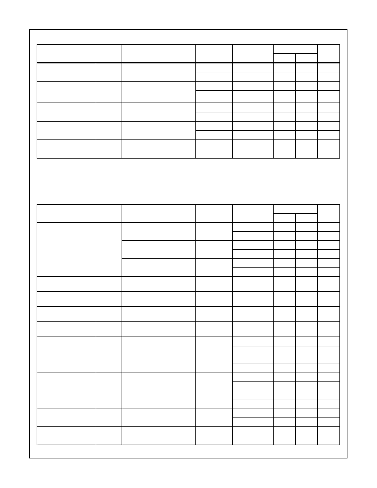
TABLE 2. AC ELECTRICAL PERFORMANCE CHARACTERISTICS
GROUP A
PARAMETER SYMBOL CONDITIONS
Propagation Delay
Parallel In to Parallel Out
Propagation Delay
3 State
AE to Out ‘A’
Propagation Delay
3-State AE to Out ‘A’
Transition Time TTHL
Maximum Clock Input
Frequency
NOTES:
1. CL = 50pF, RL = 200K, Input TR, TF < 20ns.
2. -55oC and +125oC limits guaranteed, 100% testing being implemented.
3. CL = 50pF, RL = 1K, Input TR, TF < 20ns.
PARAMETER SYMBOL CONDITIONS NOTES TEMPERATURE
Supply Current IDD VDD = 5V, VIN = VDD or GND 1, 2 -55oC, +25oC- 5 µA
Output Voltage VOL VDD = 5V, No Load 1, 2 +25oC, +125oC,
Output Voltage VOL VDD = 10V, No Load 1, 2 +25oC, +125oC,
Output Voltage VOH VDD = 5V, No Load 1, 2 +25oC, +125oC,
Output Voltage VOH VDD = 10V, No Load 1, 2 +25oC, +125oC,
Output Current (Sink) IOL5 VDD = 5V, VOUT = 0.4V 1, 2 +125oC 0.36 - mA
Output Current (Sink) IOL10 VDD = 10V, VOUT = 0.5V 1, 2 +125oC 0.9 - mA
Output Current (Sink) IOL15 VDD = 15V, VOUT = 1.5V 1, 2 +125oC 2.4 - mA
Output Current (Source) IOH5A VDD = 5V, VOUT = 4.6V 1, 2 +125oC - -0.36 mA
Output Current (Source) IOH5B VDD = 5V, VOUT = 2.5V 1, 2 +125oC - -1.15 mA
Output Current (Source) IOH10 VDD = 10V, VOUT = 9.5V 1, 2 +125oC - -0.9 mA
TPHL
TPLH
TPLZ
TPHZ
TPZL
TPZH
TTLH
FCL VDD = 5V, VIN = VDD or GND
VDD = 5V, VIN = VDD or GND
(Notes 1, 2)
VDD = 5V, VIN = VDD or GND
(Notes 2, 3)
VDD = 5V, VIN = VDD or GND
(Notes 2, 3)
VDD = 5V, VIN = VDD or GND
(Notes 1, 2)
(Note 2)
TABLE 3. ELECTRICAL PERFORMANCE CHARACTERISTICS
VDD = 10V, VIN = VDD or GND 1, 2 -55oC, +25oC- 10µA
VDD = 15V, VIN = VDD or GND 1, 2 -55oC, +25oC- 10µA
SUBGROUPS TEMPERATURE
9 +25oC - 700 ns
10, 11 +125oC, -55oC - 945 ns
9 +25oC - 400 ns
10, 11 +125oC, -55oC - 540 ns
9 +25oC - 400 ns
10, 11 +125oC, -55oC - 540 ns
9 +25oC - 200 ns
10, 11 +125oC, -55oC - 270 ns
9 +25oC 2 - MHz
10, 11 +125oC, -55oC 1.48 - MHz
+125oC - 150 µA
+125oC - 300 µA
+125oC - 600 µA
-55oC
-55oC
-55oC
-55oC
-55oC 0.64 - mA
-55oC 1.6 - mA
-55oC 4.2 - mA
-55oC - -0.64 mA
-55oC - -2.0 mA
-55oC - -1.6 mA
LIMITS
UNITSMIN MAX
LIMITS
UNITSMIN MAX
-50mV
-50mV
4.95 - V
9.95 - V
7-840
Page 5
Specifications CD4034BMS
TABLE 3. ELECTRICAL PERFORMANCE CHARACTERISTICS (Continued)
LIMITS
PARAMETER SYMBOL CONDITIONS NOTES TEMPERATURE
Output Current (Source) IOH15 VDD =15V, VOUT = 13.5V 1, 2 +125oC - -2.4 mA
-55oC - -4.2 mA
Input Voltage Low VIL VDD = 10V, VOH > 9V,
VOL < 1V
Input Voltage High VIH VDD = 10V, VOH > 9V,
VOL < 1V
Propagation Delay
Parallel In to Parallel Out
Propagation Delay
Serial to Parallel Out
Propagation Delay 3-State
AE to Out ‘A’
Propagation Delay 3-State
AE to Out ‘A’
Transition Time TTLH
Maximum Clock Input
Frequency
Minimum Data Setup
Time
Serial Data to Clock
Minimum Data Setup
Time Parallel Data to
Clock
Minimum Clock Pulse
Width
Maximum Clock Rise and
Fall Time (Note 5)
Minimum High Level
Pulse Width AE, P/S, A/S
Input Capacitance CIN Any Input 1, 2 +25oC - 7.5 pF
NOTES:
1. All voltages referenced to device GND.
2. The parameters listed on Table 3 are controlled via design or process and are not directly tested. These parameters are characterized
on initial design release and upon design changes which would affect these characteristics.
3. CL = 50pF, RL = 200K, Input TR, TF < 20ns.
4. CL = 50pF, RL = 1K, Input TR, TF < 20ns.
5. If more than one unit is cascaded, tRCL should be made less than or equal to the sum of the transition time and the fixed propagation
delay of the output of the driving stage for the estimated capacitive load.
TPHL
TPLH
TPHL
TPLH
TPLZ
TPHZ
TPZL
TPZH
TTHL
FCL VDD = 10V 1, 2, 3 +25oC 5 - MHz
TW VDD = 5V 1, 2, 3 +25oC - 250 ns
TRCL
TFCL
TW VDD = 5V 1, 2, 3 +25oC - 350 ns
VDD = 10V 1, 2, 3 +25oC - 240 ns
VDD = 15V 1, 2, 3 +25oC - 170 ns
VDD = 5V 1, 2, 3 +25oC 700 - ns
VDD = 10V 1, 2, 3 +25oC - 240 ns
VDD = 15V 1, 2, 3 +25
VDD = 10V 1, 2, 3, 4 +25
VDD = 15V 1, 2, 3, 4 +25oC - 120 ns
VDD = 10V 1, 2, 3, 4 +25oC - 160 ns
VDD = 15V 1, 2, 3, 4 +25oC - 120 ns
VDD = 10V 1, 2, 3 +25oC - 100 ns
VDD = 15V 1, 2, 3 +25oC - 80 ns
VDD = 15V 1, 2, 3 +25oC 7 - MHz
TS VDD = 5V 1, 2, 3 +25oC - 160 ns
VDD = 10V 1, 2, 3 +25oC - 60 ns
VDD = 15V 1, 2, 3 +25oC - 40 ns
TS VDD = 5V 1, 2, 3 +25oC - 50 ns
VDD = 10V 1, 2, 3 +25oC - 30 ns
VDD = 15V 1, 2, 3 +25oC - 20 ns
VDD = 10V 1, 2, 3 +25oC - 100 ns
VDD = 15V 1, 2, 3 +25oC - 70 ns
VDD = 5V 1, 2, 3 +25oC-15µs
VDD = 10V 1, 2, 3 +25oC-15µs
VDD = 15V 1, 2, 3 +25oC-15µs
VDD = 10V 1, 2, 3 +25oC - 140 ns
VDD = 15V 1, 2, 3 +25oC - 80 ns
1, 2 +25oC, +125oC,
-55oC
1, 2 +25oC, +125oC,
-55oC
o
C - 170 ns
o
C - 160 ns
-3V
+7 - V
UNITSMIN MAX
7-841
Page 6

Specifications CD4034BMS
TABLE 4. POST IRRADIATION ELECTRICAL PERFORMANCE CHARACTERISTICS
LIMITS
PARAMETER SYMBOL CONDITIONS NOTES TEMPERATURE
Supply Current IDD VDD = 20V, VIN = VDD or GND 1, 4 +25oC-25µA
N Threshold Voltage VNTH VDD = 10V, ISS = -10µA 1, 4 +25oC -2.8 -0.2 V
N Threshold Voltage
Delta
P Threshold Voltage VTP VSS = 0V, IDD = 10µA 1, 4 +25oC 0.2 2.8 V
P Threshold Voltage
Delta
Functional F VDD = 18V, VIN = VDD or GND 1 +25oC VOH >
Propagation Delay Time TPHL
NOTES: 1. All voltages referenced to device GND.
2. CL = 50pF, RL = 200K, Input TR, TF < 20ns.
∆VTN VDD = 10V, ISS = -10µA 1, 4 +25oC-±1V
∆VTP VSS = 0V, IDD = 10µA 1, 4 +25oC-±1V
VOL <
VDD = 3V, VIN = VDD or GND
VDD = 5V 1, 2, 3, 4 +25oC - 1.35 x
TPLH
3. See Table 2 for +25oC limit.
4. Read and Record
TABLE 5. BURN-IN AND LIFE TEST DELTA PARAMETERS +25OC
PARAMETER SYMBOL DELTA LIMIT
Supply Current - MSI-2 IDD ± 1.0µA
Output Current (Sink) IOL5 ± 20% x Pre-Test Reading
Output Current (Source) IOH5A ± 20% x Pre-Test Reading
VDD/2
VDD/2
+25oC
Limit
UNITSMIN MAX
ns
V
TABLE 6. APPLICABLE SUBGROUPS
MIL-STD-883
CONFORMANCE GROUP
Initial Test (Pre Burn-In) 100% 5004 1, 7, 9 IDD, IOL5, IOH5A
Interim Test 1 (Post Burn-In) 100% 5004 1, 7, 9 IDD, IOL5, IOH5A
Interim Test 2 (Post Burn-In) 100% 5004 1, 7, 9 IDD, IOL5, IOH5A
PDA (Note 1) 100% 5004 1, 7, 9, Deltas
Interim Test 3 (Post Burn-In) 100% 5004 1, 7, 9 IDD, IOL5, IOH5A
PDA (Note 1) 100% 5004 1, 7, 9, Deltas
Final Test 100% 5004 2, 3, 8A, 8B, 10, 11
Group A Sample 5005 1, 2, 3, 7, 8A, 8B, 9, 10, 11
Group B Subgroup B-5 Sample 5005 1, 2, 3, 7, 8A, 8B, 9, 10, 11, Deltas Subgroups 1, 2, 3, 9, 10, 11
Subgroup B-6 Sample 5005 1, 7, 9
Group D Sample 5005 1, 2, 3, 8A, 8B, 9 Subgroups 1, 2, 3
NOTE: 1. 5% Parameteric, 3% Functional; Cumulative for Static 1 and 2.
CONFORMANCE GROUPS
Group E Subgroup 2 5005 1, 7, 9 Table 4 1, 9 Table 4
METHOD GROUP A SUBGROUPS READ AND RECORD
TABLE 7. TOTAL DOSE IRRADIATION
MIL-STD-883
METHOD
PRE-IRRAD POST-IRRAD PRE-IRRAD POST-IRRAD
TEST READ AND RECORD
7-842
Page 7

Specifications CD4034BMS
TABLE 8. BURN-IN AND IRRADIATION TEST CONNECTIONS
OSCILLATOR
FUNCTION OPEN GROUND VDD 9V ± -0.5V
Static Burn-In 1
1 - 8 12, 15 - 23 9 - 11, 13, 14, 24
50kHz 25kHz
Note 1
Static Burn-In 2
1 - 8 12 9 - 11, 13 - 24
Note 1
Dynamic Burn-In
- 1 - 8, 11 - 14 9, 24 16 - 23 15 10
Note 1
Irradiation
1 - 8 12 9 - 11, 13 - 24
Note 2
NOTE:
1. Each pin except VDD and GND will have a series resistor of 10K ± 5%, VDD = 18V ± 0.5V
2. Each pin except VDD and GND will have a series resistor of 47K ± 5%; Group E, Subgroup 2, sample size is 4 dice/wafer, 0 failures,
VDD = 10V ± 0.5V
Logic Diagram
*
AB
N
N
MM
AE
P/S
A/S
CLOCK
M
L
*
P/S
K
K
L
*
P/S
CLS
*
CLS
CLM
*INPUTS PROTECTED BY
CMOS PROTECTION
*
CLM
FLIP-FLOP TRUTH TABLE
INPUTS OUTPUT
CLM CLS D Q
00
00
0 Invalid Condition
X0
11
11
1 Invalid Condition
1 = High Level 0 = Low Level X = Don’t Care
NETWORK
VDD
VSS
7-843
Page 8

CD4034BMS
“A” OR “B”
DATA
INPUTS
“B” OR “A”
DATA
OUTPUTS
tPLH
tTLH tTHL
tPHL
90%
50%
10%
0
FIGURE 1. ASYNCHRONOUS OPERATION PROPAGATION
DELAY TIME AND TRANSITION TIME
CLOCK
A ENABLE
P/S
A/B
A/S
VDD
trCL tfCL
CLOCK
INPUT
INPUT
**
tSLH
OUTPUT
tTLH
tPLH tPHL
**
tSHL
tTHL
VDD
90%
50%
10%
50%
VDD
90%
50%
10%
*Input refers to any of the “A” or “B” data inputs, “A” ENABLE,
SERIAL INPUT, A/B, P/S, or A/S inputs
**tSLH and tSHL are Set-Up times
FIGURE 2. SYNCHRONOUS OPERATION PROPAGATION DE-
LAY TIMES, TRANSITION TIMES, AND SET-UP
TIMES
0
0
0
SERIAL DATA
A1
A2
A3
A4
A5
A6
A7
A8
B1
B2
B3
B4
B5
B6
B7
B8
B DATA LINES ARE OUTPUTS
A DATA
LINES ARE
OUTPUTS
FIGURE 3. TIMING DIAGRAM
7-844
Page 9

Typical Performance Characteristics
CD4034BMS
AMBIENT TEMPERATURE (TA) = +25oC
30
GATE-TO-SOURCE VOLTAGE (VGS) = 15V
25
20
15
10V
10
5
OUTPUT LOW (SINK) CURRENT (IOL) (mA)
5V
0 5 10 15
DRAIN-TO-SOURCE VOLTAGE (VDS) (V)
FIGURE 4. TYPICAL OUTPUT LOW (SINK) CURRENT
CHARACTERISTICS
DRAIN-TO-SOURCE VOLTAGE (VDS) (V)
AMBIENT TEMPERATURE (TA) = +25oC
GATE-TO-SOURCE VOLTAGE (VGS) = -5V
-10V
AMBIENT TEMPERATURE (TA) = +25oC
15.0
12.5
GATE-TO-SOURCE VOLTAGE (VGS) = 15V
10.0
7.5
10V
5.0
2.5
OUTPUT LOW (SINK) CURRENT (IOL) (mA)
5V
0 5 10 15
DRAIN-TO-SOURCE VOLTAGE (VDS) (V)
FIGURE 5. MINIMUM OUTPUT LOW (SINK) CURRENT
CHARACTERISTICS
0-5-10-15
0
-5
-10
-15
-20
DRAIN-TO-SOURCE VOLTAGE (VDS) (V)
AMBIENT TEMPERATURE (TA) = +25oC
GATE-TO-SOURCE VOLTAGE (VGS) = -5V
-10V
0-5-10-15
0
-5
-10
-25
-15V
-30
FIGURE 6. TYPICAL OUTPUT HIGH (SOURCE) CURRENT
CHARACTERISTICS
AMBIENT TEMPERATURE (TA) = +25oC
200
150
SUPPLY VOLTAGE (VDD) = 5V
100
10V
50
TRANSITION TIME (tTHL, tTLH) (ns)
0
0 40 60 80 10020
15V
LOAD CAPACITANCE (CL) (pF)
FIGURE 8. TYPICAL TRANSITION TIME AS A FUNCTION OF
LOAD CAPACITANCE
-15V
OUTPUT HIGH (SOURCE) CURRENT (IOH) (mA)
FIGURE 7. MINIMUM OUTPUT HIGH (SOURCE) CURRENT
CHARACTERISTICS
6
10
AMBIENT TEMPERATURE (TA) = +25oC
8
6
4
2
SUPPLY VOLTAGE (VDD) = 15V
5
10
8
6
4
2
4
10
8
6
4
2
3
10
8
6
4
2
POWER DISSIPATION PER GATE (PD) (µW)
2
10
86428642
11010
2
5V
CL = 50pF
CL = 15pF
8642
3
10
10V
INPUT FREQUENCY (fI) (kHz)
FIGURE 9. TYPICAL DYNAMIC POWER DISSIPATION AS A
FUNCTION OF CLOCK FREQUENCY
10V
86428642
4
10
-15
OUTPUT HIGH (SOURCE) CURRENT (IOH) (mA)
5
10
7-845
Page 10

CD4034BMS
Typical Performance Characteristics (Continued)
AMBIENT TEMPERATURE (TA) = +25oC
700
600
500
400
300
SUPPLY VOLTAGE (VDD) = 5V
200
100
[A(B) PAR DATA IN B(A) PAR DATA OUT]
PROPAGATION DELAY TIME (tPHL, tPLH) (ns)
0304020
LOAD CAPACITANCE (CL) (pF)
50 60 70 80 90 100
10V
15V
FIGURE 10. TYPICAL PROPAGATION DELAY TIME AS A FUNC-
TION OF LOAD CAPACITANCE [A(B) PARALLEL
DATA INPUT TO B(A) PARALLEL DATA OUTPUT,
SYNCHRONOUS OR ASYNCHRONOUS])
7-846
Page 11

VSS
PROTECTION NETWORK
ON ALL “A” AND “B”
DATA INPUTS
P/S
CLM
CD4034BMS
K
p
n
K
An
CLS
1 OF 8 STAGES
Q’
M
Q’
VDD
SERIAL
DATA
VDD
VSS
PROTECTION NETWORK
ON SERIAL DATA INPUT
D
p
n
P/S
p
n
CLM
CLM
p
n
CLM
L
p
n
L
CLS
Bn
p
n
CLS
p
n
CLS
M
N
Q’
N
Q (TO NEXT STAGE D)
FIGURE 11. REGISTER STAGE LOGIC DIAGRAM (1 OF 8 STAGES)
TRUTH TABLE REGISTER INPUT-LEVELS AND
RESULTING REGISTER OPERATION
“A”
ENABLE P/S A/B A/S OPERATION*
0 0 0 X Serial Mode; Synch. Serial Data Input, “A” Parallel Data Outputs Disabled
0 0 1 X Serial Mode; Synch. Serial Data Input, “B” Parallel Data Output
0 1 0 0 Parallel Mode; “B” Synch. Parallel Data Inputs, “A” Parallel Data Outputs Disabled
VSS
VDD
VSS
0 1 0 1 Parallel Mode; “B” Asynch. Parallel Data Inputs, “A” Parallel Data Outputs Disabled
0 1 1 0 Parallel Mode; “A” Parallel Data Inputs Disabled, “B” Parallel Data Outputs, Synch. Data
Recirculation
0 1 1 1 Parallel Mode; “A” Parallel Data Inputs Disabled, “B” Parallel Data Outputs, Asynch. Data
Recirculation
1 0 0 X Serial Mode; Synch. Serial Data Input, “A” Parallel Data Output
1 0 1 X Serial Mode; Synch. Serial Data Input, “B” Parallel Data Output
1 1 0 0 Parallel Mode; “B” Synch. Parallel Data Input, “A” Parallel Data Output
1 1 0 1 Parallel Mode; “B” Asynch. Parallel Data Input, “A” Parallel Data Output
1 1 1 0 Parallel Mode; “A” Synch, Parallel Data Input, “B” Parallel Data Output
1 1 1 1 Parallel Mode; “A” Asynch. Parallel Data Input, “B” Parallel Data Output
*Outputs change at positive transition of clock in the serial mode and when the A/S control input is “low” in the parallel mode. During
transfer from parallel to serial operation A/S should remain low in order to prevent DS transfer into Flip Flops.
1 = High Level 0 = Low Level X = Don’t Care
7-847
Page 12

Applications
VDD
CD4034BMS
VDD
SERIAL
DATA
P/S
A/S
CL
VDD
AE
A PARALLEL
SI
A/B
CD4034
A/S
B PARALLEL
CL
P/S
DATA
DATA
SERIAL
DATA
VDD
AE
A PARALLEL
SI
A/B
A/S
B PARALLEL
CL
P/S
DATA
CD4034
DATA
SERIAL
FIGURE 12. 16-BIT PARALLEL IN/PARALLEL OUT, P ARALLEL IN/SERIAL OUT,
SERIAL IN/PARALLEL OUT SERIAL IN/SERIAL OUT REGISTER
“A” ENABLE
SERIAL
DATA
A/B
CL
AE
A PARALLEL
SI
A/B
CD4034
A/S
B PARALLEL
CL
P/S
DATA
DATA
SERIAL
DATA
AE
A PARALLEL
SI
A/B
A/S
B PARALLEL
CL
P/S
DATA
CD4034
DATA
DATA
SERIAL
DATA
MEMORY
UNIT
PERIPHERAL
UNIT
FIGURE 13. 16-BIT SERIAL IN/GATED PARALLEL OUT REGISTER
P/S
1
CD4034
2
W REG
3
4
B A
5
6
7
8
SI A/B A/S CL
SI A/B A/S CL
P/S
1
2
Y REG
3
4
B A
5
CD4034
6
7
8
AE
AE
BUS LINES
(SINGLE)
1
2
3
4
5
6
7
8
1
2
3
4
5
6
7
8
DOUBLE - BUS SYSTEM
(ENABLE INPUTS ON BOTH SIDES)
AE
1
2
3
4
5
6
7
8
SI A/B A/S CL
SI A/B A/S CL
AE
1
2
3
4
5
6
7
8
X(1)
REG
A
CD4034
Z REG
A
CD4034
P/S
B
P/S
1
2
3
4
5
6
7
8
P/S
1
2
3
4
5
6
7
8
SI A/B A/S CL
1
2
3
4
5
6
7
8
B
AE
1
2
X(2)
3
REG
UNIT
4
A
5
6
7
8
B
CD4034
ARITHMETIC
TO 2ND
BUS
SYSTEM
THE “A” ENABLE (AE) AND A/B SIGNALS CONTROL ALL
COMBINATIONS OF TRANSFER BETWEEN THE REGISTERS
AND BUS SYSTEMS
FIGURE 14. SINGLE AND DOUBLE-BUS SYSTEMS
7-848
Page 13

Applications (Continued)
SHIFT LEFT OUTPUT
“A” ENABLE
SHIFT LEFT/
SHIFT RIGHT
SHIFT RIGHT
INPUT
REG. 1
CLOCK
A/S
PARALLEL
ENTRY
CD4034
VDD
SI
P/S
A/S
CL
SI
P/S
A/S
CL
AE
A/B
AE
A/B
“A” PARALLEL DATA
1
1
1
REG. 3
CD4034
1
CD4034BMS
8
8A PARALLEL DATA
8B PARALLEL DATA
VDD
SI
P/S
A/S
CL
SI
P/S
A/S
CL
AE
A/B
AE
A/B
“A” PARALLEL DATA
1
1
1
REG. 4
CD4034
1
AE
P/S
SHIFT RIGHT
OUTPUT
8
REG. 2
CD4034
SHIFT
LEFT INPUT*
A/S
CL
AE
8A PARALLEL DATA
8B PARALLEL DATA
FIGURE 15. SHIFT RIGHT/SHIFT LEFT WITH PARALLEL INPUTS
A “High” (“Low”) on the shift Left/Shift Right input allows
serial data on the Shift Left Input (Shift Right Input) to enter
the register on the positive transition of the clock signal. A
“high” on the “A” Enable Input disables the “A” parallel data
lines Reg. 1 and 2 and enables the “A” data lines on registers 3 and 4 and allows parallel data into registers 1 and 2.
SERIAL
DATA
VDD
CLOCK
FIGURE 16. N-STAGE SHIFT REGISTER WITH FIXED SERIAL
AE
SI
A/B
A/S
CL
P/S
CD4016
OUTPUT LINE
A PARALLEL DATA
CD4034
B PARALLEL DATA
N STAGE SELECTION
CD4016
N = 1 - 8
SERIAL
OUTPUT
Other logic schemes may be used in place of registers 3 and
4 for parallel loading.
When parallel inputs are not used Reg. 3 and 4 and associated logic are not required.
* Shift left input must be disabled during parallel entry.
SAMPLE/HOLD
AE
18
SERIAL DATA
VDD
A/S
CLOCK
P/S
SI
A/B
A/S
CL
P/S
FIGURE 17. SAMPLE AND HOLD REGISTER - SERIAL/PARAL-
LEL IN - PARALLEL OUT
“A” PARALLEL DATA
CD4034
“B” PARALLEL DATA
18
TO DISPLAY ETC
7-849
Page 14

Chip Dimensions and Pad Layout
CD4034BMS
Dimension in parenthesis are in millimeters and are
derived from the basic inch dimensions as indicated.
Grid graduations are in mils (10
-3
inch).
METALLIZATION: Thickness: 11kÅ − 14kÅ, AL.
PASSIVATION: 10.4kÅ - 15.6kÅ, Silane
BOND PADS: 0.004 inches X 0.004 inches MIN
DIE THICKNESS: 0.0198 inches - 0.0218 inches
All Intersil semiconductor products are manufactured, assembled and tested under ISO9000 quality systems certification.
Intersil products are sold by description only. Intersil Corporation reserves the right to make changes in circuit design and/or specifications at any time without
notice. Accordingly, the reader is cautioned to verify that data sheets are current before placing orders. Information furnished by Intersil is believed to be accurate
and reliable. However, no responsibility is assumed by Intersil or its subsidiaries for its use; nor for any infringements of patents or other rights of third parties which
may result from its use. No license is granted by implication or otherwise under any patent or patent rights of Intersil or its subsidiaries.
For information regarding Intersil Corporation and its products, see web site http://www.intersil.com
Sales Office Headquarters
NORTH AMERICA
Intersil Corporation
P. O. Box 883, Mail Stop 53-204
Melbourne, FL 32902
TEL: (321) 724-7000
FAX: (321) 724-7240
EUROPE
Intersil SA
Mercure Center
100, Rue de la Fusee
1130 Brussels, Belgium
TEL: (32) 2.724.2111
FAX: (32) 2.724.22.05
ASIA
Intersil (Taiwan) Ltd.
Taiwan Limited
7F-6, No. 101 Fu Hsing North Road
Taipei, Taiwan
Republic of China
TEL: (886) 2 2716 9310
FAX: (886) 2 2715 3029
850
 Loading...