

Page 1
October 1987
Revised January 1999
CD4030C Quad EXCLUSIVE-OR Gate
© 1999 Fairchild Semiconductor Corporation DS005961.prf www.fairchildsemi.com
CD4030C
Quad EXCLUSIVE-OR Gate
General Description
The CD4030C EXCLU SIVE-O R gat es are monol ithi c complementary MOS (CMOS) integrated circuits c onstructed
with N- and P-channel enha ncement mode transist ors. All
inputs are protected against static discharge with diodes to
V
DD
and VSS.
Features
■ Wide supply voltage range: 3.0V to 15V
■ Low power: 100 nW (typ.)
■ Medium speed operation:
t
PHL
= t
PLH
= 40 ns (typ.) at CL = 15 pF, 10V supply
■ High noise immunity 0.45 V
CC
(typ.)
Applications
• Automotive
• Data terminals
• Instrumentation
• Medical electronics
• Industrial controls
• Remote metering
• Computers
Ordering Code:
Device also available in Tape and Reel. Specify by appendin g s uf f ix let t er “X” to the ordering co de.
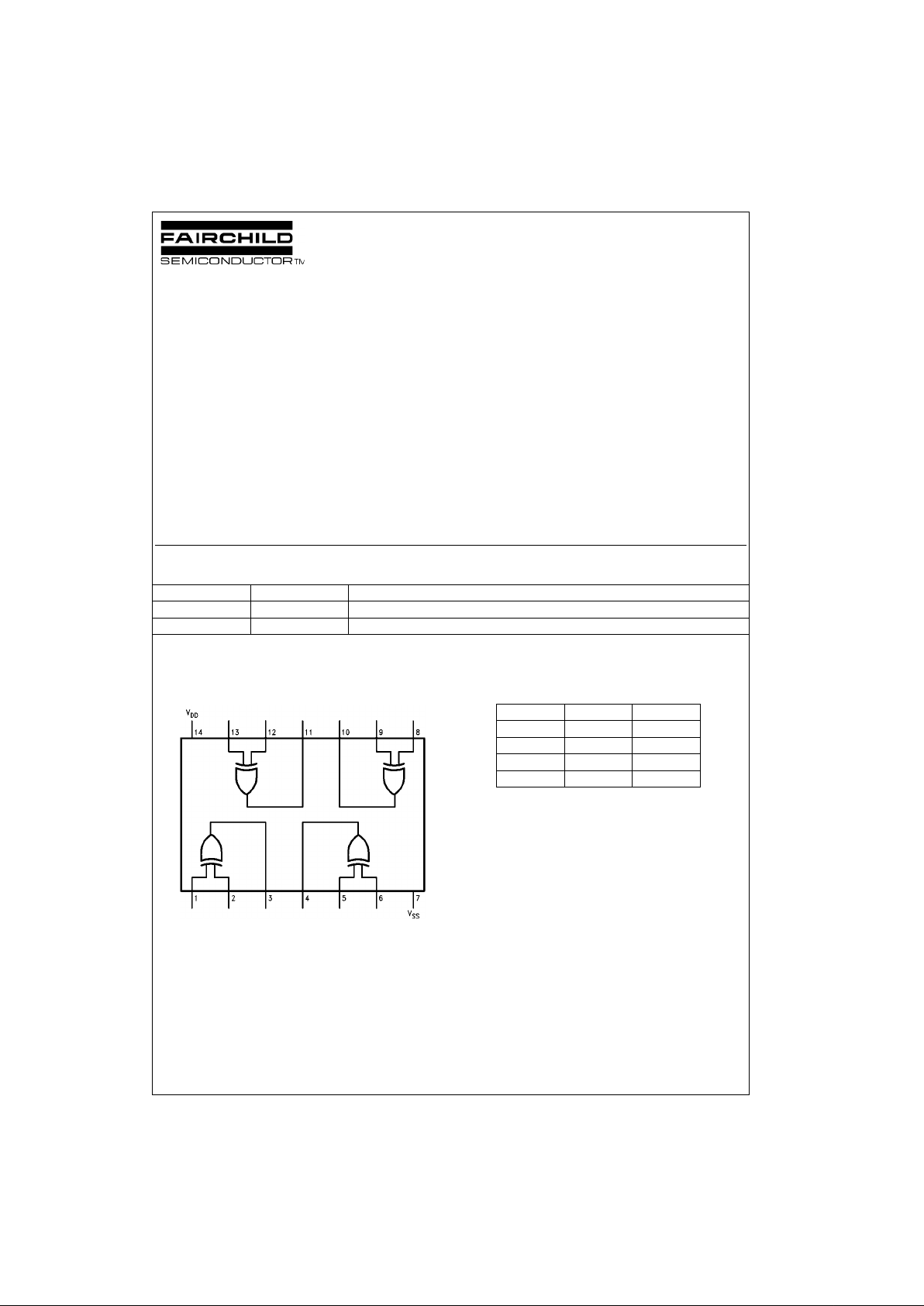
Connection Diagram
Pin Assignments for DIP and SOP
Truth Table
1 = HIGH Level
0 = LOW Level
Order Number Package Number Package Description
CD4030CSJ M14D 14-Lead Small Outline Package (SOP), EIAJ TYPE II, 5.3mm Wide
CD4030CN N14A 14-Lead Plastic Dual-In-Line Package (PDIP), JEDEC MS-001, 0.300” Wide
A B J
0 0 0
1 0 1
0 1 1
1 1 0
Page 2
www.fairchildsemi.com 2
CD4030C
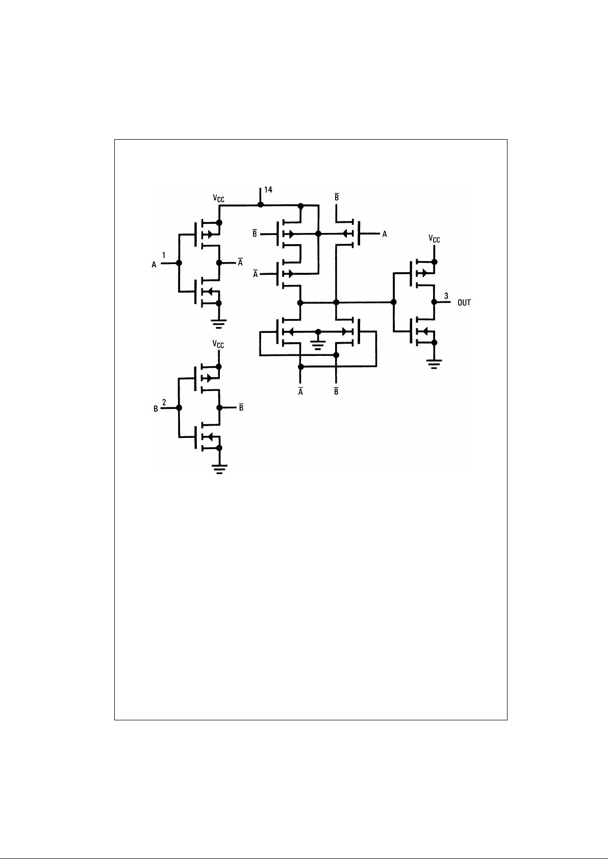
Logic Diagram
Page 3

3 www.fairchildsemi.com
CD4030C
Absolute Maximum Ratings(Note 1)
Note 1: “Absolute Maximum Rat ings” are tho se values beyond which the
safety of the device cannot be guaranteed. E x c ept for “ Operating Temperature Range” they are not mea nt to imply that the devices sh ould be operated at these limits. The Electrical Charac t eristics tables provide conditions
for actual device operation.
Note 2: This device should not be connecte d to circuits with power on
because high transie nt voltages may cause permanent damage.
DC Electrical Characteristics
Note 3: IDN and IDP are tested one output at a time.
AC Electrical Characteristics (Note 4)
Note 4: AC Parameters are guaranteed by DC correlated testing.
Voltage at Any Pin (Note 2) VSS −0.3V to VSS +15.5V
Operating Temperature Range −40°C to +85°C
Storage Temperature Range −65°C to +150°C
Power Dissipation (P
D
)
Dual-In-Line 700 mW
Small Outline 500 mW
Operating V
DD
Range VSS +3.0V to VSS +15V
Lead Temperature
(Soldering, 10 seconds) 260°C
Limits
Symbol Parameter Conditions −40°C +25°C +85°CUnits
Min Typ Max Min Typ Max Min Typ Max
I
L
Quiescent Device VDD = 5.0V 5.0 0.05 5.0 70 µA
Current VDD = 10V 10 0.1 10 140 µA
P
D
Quiescent Device VDD = 5.0V 25 0.25 25 350 µW
Dissipation Package VDD = 10V 100 1.0 100 1,400 µW
V
OL
Output Voltage VDD = 5.0V 0.05 0 0.05 0.05 V
LOW Level VDD = 10V 0.05 0 0.05 0.05 V
V
OH
Output Voltage VDD = 5.0V 4.95 4.95 5.0 4.95 V
HIGH Level VDD = 10V 9.95 9.95 10 9.95 V
V
NL
Noise Immunity VDD = 5.0V 1.5 1.5 2.25 1.4 V
(All Inputs) VDD = 10V 3.0 3.0 4.5 2.9 V
V
NH
Noise Immunity VDD = 5.0V 1.4 1.5 2.25 1.5 V
(All Inputs) VDD = 10V 2.9 3.0 4.5 3.0 V
IDN Output Drive Current VDD = 5.0V 0.35 0.3 1.2 0.25 mA
N-Channel (Note 3) VDD = 10V 0.7 0.6 2.4 0.5 mA
IDP Output Drive Current VDD = 5.0V −0.21 −0.15 −0.6 −0.12 mA
P-Channel (Note 3) VDD = 10 V −0.45 −0.32 −1.3 −0.25 mA
I
I
Input Current VI = 0V or VI = V
DD
10 pA
Symbol Parameter Conditions
Limits
Units
Min Typ Max
t
PHL
Propagation Delay Time VDD = 5.0V 100 300 ns
VDD = 10V 40 150 ns
t
PLH
Propagation Delay Time VDD = 5.0V 100 300 ns
VDD = 10V 40 150 ns
t
THL
Transition Time VDD = 5.0V 70 300 ns
HIGH-to-LOW Level VDD = 10V 25 150 ns
t
TLH
Transition Time VDD = 5.0V 80 300 ns
LOW-to-HIGH Level VDD = 10V 30 150 ns
C
I
Input Capacitance VI = 0V or VI = V
DD
5.0 pF
Page 4

www.fairchildsemi.com 4
CD4030C
Physical Dimensions inches (millimeters) unless otherwise noted
14-Lead Small Outline Package (SOP), EIAJ TYPE II, 5.3mm Wide
Package Number M14D
Page 5

Fairchild does not assume any responsibility for use of any circuitry described, no circuit patent licenses are implied and Fairchild reserves the right at any time without notice to change said circuitry and specifications.
CD4030C Quad EXCLUSIVE-OR Gate
LIFE SUPPORT POLICY
FAIRCHILD’S PRODUCTS ARE NOT AUTHORIZED FOR USE AS CRITICAL COMPONENTS IN LIFE SUPPORT
DEVICES OR SYSTEMS WITHOUT THE EXPRESS WRITTEN APPROVAL OF THE PRESIDENT OF FAIRCHILD
SEMICONDUCTOR CORPORATION. As used herein:
1. Life support devices or system s a re devices or syste ms
which, (a) are intended for surgical implant into the
body, or (b) support or sustain life, and (c) whose failure
to perform when properly used in accordance with
instructions for use provided in the labeling, can be reasonably expected to result in a significant injur y to the
user.
2. A critical compon ent in any com ponent of a li fe support
device or system whose failure to p erform can be r easonably expected to cause the failure of the life suppor t
device or system, or to affect its safety or effectiveness.
www.fairchildsemi.com
Physical Dimensions inches (millimeters) unless otherwise noted (Continued)
14-Lead Plastic Dual-In-Line Package (PDIP), JEDEC MS-001, 0.300” Wide
Package Number N14A
 Loading...