

Datasheet CD4029BCWMX, CD4029BCWM, CD4029BCSJX, CD4029BCSJ, CD4029BCNMC14029BCP Datasheet (Fairchild Semiconductor)
Page 1
October 1987
Revised January 1999
CD4029BC Presettable Binary/Decade Up/Down Counter
© 1999 Fairchild Semiconductor Corporation DS005960.prf www.fairchildsemi.com
CD4029BC
Presettable Binary/Decade Up/Down Counter
General Description
The CD4029BC is a presettable up/down counte r which
counts in either binar y or decade mode de pending on the
voltage level applied at binary/ decade input. W hen binar y/
decade is at logical “1”, the co un ter coun ts in bina ry, otherwise it counts in decade. Similar ly, the counter counts up
when the up/down input is at logical “1” and vice versa.
A logical “1” preset enable signal allows infor mation at the
“jam” inputs to preset the counter to any state asyn chronously with the clock. The coun ter is advanced one count
at the positive-going edg e of the clock if the carry in and
preset enable inputs are at logical “0”. Advancement is
inhibited when either or both of these two inputs is at logical “1”. The carry out signal is norma lly at logical “1” state
and goes to logical “0” state when the counter reaches its
maximum count in the “up” mode or the minimum count in
the “down” mode provi ded the carr y input is at log ical “0”
state.
All inputs are protected against static discharge by diode
clamps to both V
DD
and VSS.
Features
■ Wide supply voltage range: 3V to 15V
■ High noise immunity: 0.45 V
DD
(typ.)
■ Low power TTL compatibility: fan out of 2 driving 74L
or 1 driving 74LS
■ Parallel jam inputs
■ Binary or BCD decade up/down counting
Ordering Code:
Devices also available in Tape and Reel. Specify by appending the suffix letter “X” to t he ordering code.
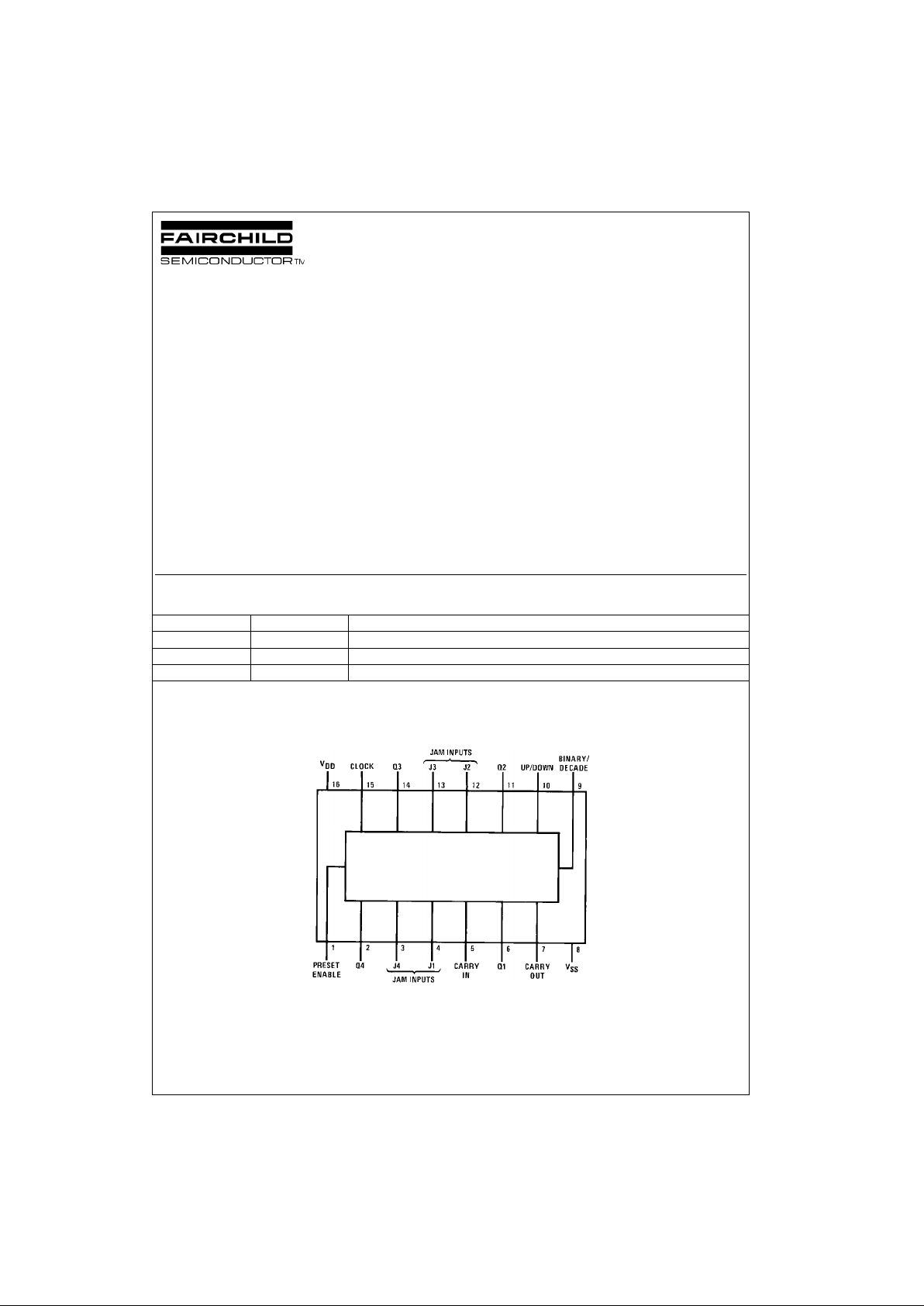
Connection Diagram
Pin Assignments for DIP, SOIC and SOP
Top View
Order Number Package Number Package Description
CD4029BCWM M16B 16-Lead Small Outline Integrated Circuit (SOIC), JEDEC MS-013, 0.300” Wide body
CD4029BCSJ M16D 16-Lead Small Outline Package (SOP), EIAJ TYPE II, 5.3mm Wide
CD4029BCN N16E 16-Lead Plastic Dual-In-Line Package (PDIP), JEDEC MS-001, 0.300” Wide
Page 2
www.fairchildsemi.com 2
CD4029BC
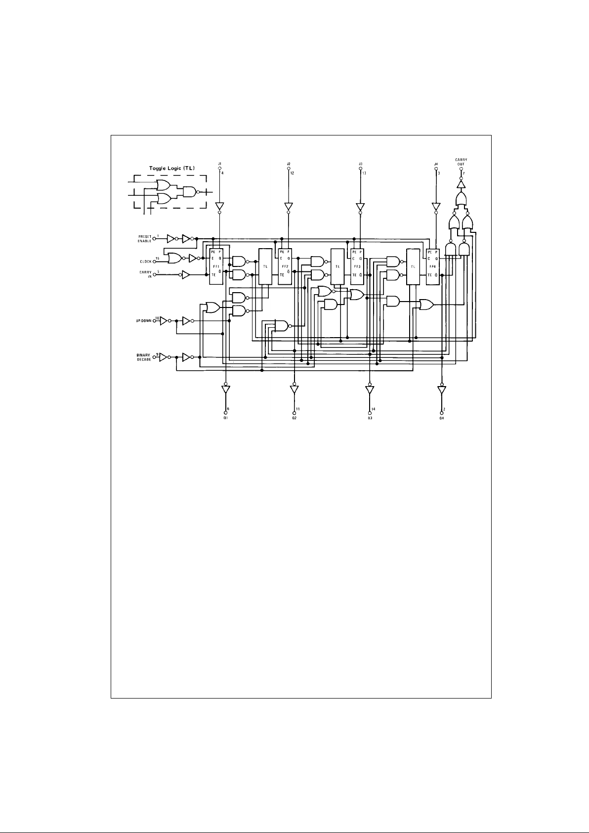
Logic Diagram
Page 3
3 www.fairchildsemi.com
CD4029BC
Absolute Maximum Ratings(Note 1)
(Note 2)
Recommended Operating
Conditions
(Note 2)
Note 1: “Absolute Maximum Rat ings” are tho se values beyond which the
safety of the device cannot be guaranteed. E x c ept for “ Operating Temperature Range” they are not mea nt to imply that the devices sh ould be operated at these limits. The table of “Electrical Characteristics” provides
conditions for actual device o peration.
Note 2: V
SS
= 0V unless otherw is e s pecified.
DC Electrical Characteristics (Note 2)
Note 3: IOH and IOL are tested one output at a ti m e.
DC Supply Voltage (VDD) −0.5V to +18 V
DC
Input Voltage (VIN) −0.5V to VDD + 0.5 V
DC
Storage Temperature Range (TS) −65°C to +150°C
Power Dissipation (P
D
)
Dual-In-Line 700 mW
Small Outline 500 mW
Lead Temperature (T
L
)
(Soldering, 10 seconds) 260°C
DC Supply Voltage (V
DD
) 3V to 15 V
DC
Input Voltage (VIN) 0V to VDD V
DC
Operating Temperature Range (TA) −40°C to +85°C
Symbol Parameter Conditions
−40°C +25°C +85°C
Units
Min Max Min Typ Max Min Max
I
DD
Quiescent Device Current VDD = 5V 20 20 150 µA
VDD = 10V 40 40 300 µA
VDD = 15V 80 80 600 µA
V
OL
LOW Level |IO| < 1 µA
Output Voltage VDD = 5V 0.05 0 0.05 0.05 V
VDD = 10V 0.05 0 0.05 0.05 V
VDD = 15V 0.05 0 0.05 0.05 V
V
OH
HIGH Level |IO| < 1 µA
Output Voltage VDD = 5V 4.95 4.95 5 4.95 V
VDD = 10V 9.95 9.95 10 9.95 V
VDD = 15V 14.95 14.95 15 14.95 V
V
IL
LOW Level VDD = 5V, VO = 0.5V or 4.5V 1.5 1.5 1.5 V
Input Voltage VDD = 10V, VO = 1V or 9V 3.0 3.0 3.0 V
VDD = 15V, VO = 1.5V or 13.5V 4.0 4.0 4.0 V
V
IH
HIGH Level VDD = 5V, VO = 0.5V or 4.5V 3.5 3.5 3.5 V
Input Voltage VDD = 10V, VO = 1V or 9V 7.0 7.0 7.0 V
VDD = 15V, VO = 1.5V or 13.5V 11.0 11.0 11.0 V
I
OL
LOW Level Output VDD = 5V, VO = 0.4V 0.52 0.44 0.88 0.36 mA
Current (Note 3) VDD = 10V, VO = 0.5V 1.3 1.1 2.25 0.9 mA
VDD = 15V, VO = 1.5V 3.6 3.0 8.8 2.4 mA
I
OH
HIGH Level Output VDD = 5V, VO = 4.6V −0.52 −0.44 −0.88 −0.36 mA
Current (Note 3) VDD = 10V, VO = 9.5V −1.3 −1.1 −2.25 −0.9 mA
VDD = 15V, VO = 13.5V −3.6 −3.0 −8.8 −2.4 mA
I
IN
Input Current VDD = 15V, VIN = 0V −0.3 −10−5−0.3 −1.0 µA
VDD = 15V, VIN = 15V 0.3 10−50.3 1.0 µA
Page 4

www.fairchildsemi.com 4
CD4029BC
AC Electrical Charac teristics (Note 4)
TA = 25°C, CL = 50 pF, RL = 200k, Input t
rCL
= t
fCL
= 20 ns, unless otherwise specified
Note 4: *AC Parameters are guaranteed by DC correlated t es t ing.
Note 5: C
PD
determines the no lo ad AC power consump tion of any CMOS device. For comple te explanatio n, see 74C Family Ch aracteris tics application
note, AN-90.
Symbol Parameter Conditions Min Typ Max Units
CLOCKED OPERATION
t
PHL
or t
PLH
Propagation Delay Time VDD = 5V 200 400 ns
to Q Outputs VDD = 10V 85 170 ns
VDD = 15V 70 140 ns
t
PHL
or t
PLH
Propagation Delay Time VDD = 5V 320 640 ns
to Carry Output VDD = 10V 135 270 ns
VDD = 15V 110 220 ns
t
PHL
or t
PLH
Propagation Delay Time CL = 15 pF
to Carry Output VDD = 5V 285 570 ns
VDD = 10V 120 240 ns
VDD = 15V 95 190 ns
t
THL
or t
TLH
Transition Time/Q VDD = 5V 100 200 ns
or Carry Output VDD = 10V 50 100 ns
VDD = 15V 40 80 ns
tWH or t
WL
Minimum Clock VDD = 5V 160 320 ns
Pulse Width VDD = 10V 70 135 ns
VDD = 15V 55 110 ns
t
rCL
or t
fCL
Maximum Clock Rise VDD = 5V 15 µs
and Fall Time VDD = 10V 10 µs
VDD = 15V 5 µs
t
SU
Minimum Set-Up Time VDD = 5V 180 360 ns
VDD = 10V 70 140 ns
VDD = 15V 55 110 ns
f
CL
Maximum Clock Frequency VDD = 5V 1.5 3.1 MHz
VDD = 10V 3.7 7.4 MHz
VDD = 15V 4.5 9 MHz
C
IN
Average Input Capacitance Any Input 5 7.5 pF
C
PD
Power Dissipation Capacitance Per Package (Note 5) 65 pF
PRESET ENABLE OPERATION
t
PHL
or t
PLH
Propagation Delay Time VDD = 5V 285 570 ns
to Q output VDD = 10V 115 230 ns
VDD = 15V 95 195 ns
t
PHL
or t
PLH
Propagation Delay Time VDD = 5V 400 800 ns
to Carry Output VDD = 10V 165 330 ns
VDD = 15V 135 260 ns
t
WH
Minimum Preset Enable VDD = 5V 80 160 ns
Pulse Width VDD = 10V 30 60 ns
VDD = 15V 25 50 ns
t
REM
Minimum Preset Enable VDD = 5V 150 300 ns
Removal Time VDD = 10V 60 120 ns
VDD = 15V 50 100 ns
CARRY INPUT OPERATION
t
PHL
or t
PLH
Propagation Delay Time VDD = 5V 265 530 ns
to Carry Output VDD = 10V 110 220 ns
VDD = 15V 90 180 ns
t
PHL
, t
PLH
Propagation Delay Time CL = 15 pF
to Carry Output VDD = 5V 200 400 ns
VDD = 10V 85 170 ns
VDD = 15V 70 140 ns
Page 5
5 www.fairchildsemi.com
CD4029BC
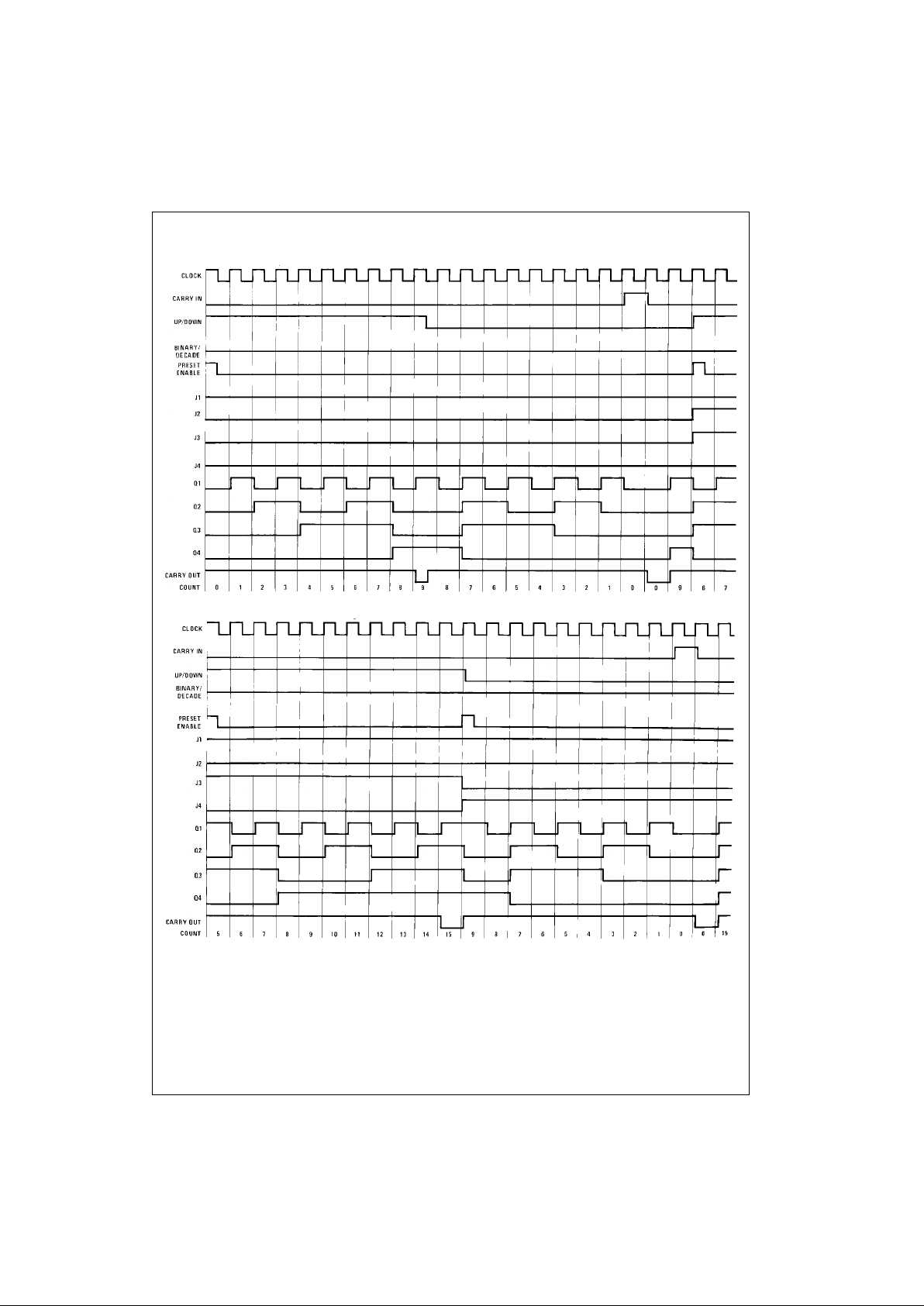
Logic Waveforms
Decade Mode
Binary Mode
Page 6

www.fairchildsemi.com 6
CD4029BC
Switching Time Waveforms
Cascading Packages
Parallel Clocking
Ripple Clocking
Carry out lines at the 2nd or later sta ges may have a negative-going spike due to differential int er nal delays. These spikes
do not affect counter operation, but if the carry out is used to trigger external circuitry the carry out should be gated with the
clock.
Page 7

7 www.fairchildsemi.com
CD4029BC
Physical Dimensions inches (millimeters) unless otherwise noted
16-Lead Small Outline Integrated Circuit (SOIC), JEDEC MS-013, 0.300” Wide Body
Package Number M16B
16-Lead Small Outline Package (SOP), EIAJ TYPE II, 5.3mm Wide
Package Number M16D
Page 8

Fairchild does not assume any responsibility for use of any circuitry described, no circuit patent licenses are implied and Fairchild reserves the right at any time without notice to change said circuitry and specifications.
CD4029BC Presettable Binary/Decade Up/Down Counter
LIFE SUPPORT POLICY
FAIRCHILD’S PRODUCTS ARE NOT AUTHORIZED FOR USE AS CRITICAL COMPONENTS IN LIFE SUPPORT
DEVICES OR SYSTEMS WITHOUT THE EXPRESS WRITTEN APPROVAL OF THE PRESIDENT OF FAIRCHILD
SEMICONDUCTOR CORPORATION. As used herein:
1. Life support devices or system s ar e devices or syste ms
which, (a) are intended for surgical implant into the
body, or (b) support or sustain life, and (c) whose failure
to perform when properly used in accordance with
instructions for use provided in the labeling, can be reasonably expected to result in a significant injury to the
user.
2. A critical component in any c omponent of a life suppor t
device or system whose failure to perform can be reasonably expected to cause the failure of the life suppor t
device or system, or to affect its safety or effectiveness.
www.fairchildsemi.com
Physical Dimensions inches (millimeters) unless otherwise noted (Continued)
16-Lead Plastic Dual-In-Line Package (PDIP), JEDEC MS-001, 0.300” Wide
Package Number N16E
 Loading...