

Page 1

October 1987
Revised January 1999
CD4027BC Dual J-K Master/Slave Flip-Flop with Set and Reset
© 1999 Fairchild Semiconductor Corporation DS005958.prf www.fairchildsemi.com
CD4027BC
Dual J-K Master/Slave Flip-Flop with Set and Reset
General Description
The CD4027BC dual J-K flip-flops are monolithic complementary MOS (CMOS) integrated circuits constructed with
N- and P-channel enhancement mode transistors. Each
flip-flop has indepe ndent J, K, set, reset, and clock inputs
and buffered Q and Q
outputs. These flip-flops ar e edge
sensitive to the clock input and change stat e on the positive-going transition of the clock pulses. Set or reset is
independent of the clock and is accomplished by a high
level on the respective input.
All inputs are protected a gainst damage due to static discharge by diode clamps to V
DD
and VSS.
Features
■ Wide supply voltage range: 3.0V to 15V
■ High noise immunity: 0.45 V
DD
(typ.)
■ Low power TTL compatibility: Fan out of 2 driving 74L
or 1 driving 74LS
■ Low power: 50 nW (typ.)
■ Medium speed operation: 12 MHz (typ.) with 10V
supply
Ordering Code:
Devices also available in Tape and Reel. Specify by appending the suffix letter “X” to the ordering code.
Connection Diagram
Pin Assignments for DIP and SOIC
Top View
Truth Table
I = HIGH Level
O = LOW Level
X = Don't Care
= LOW-to-HIGH
= HIGH-to-LOW
Note 1: t
n−1
refers to the time interval p rior to the positive clock pulse
transition
Note 2: t
n
refers to the time intervals after the positive clock pulse
transition
Note 3: Level Change
Order Number Package Number Package Description
CD4027BCM M16A 16-Lead Small Outline Integrated Circuit (SOIC), JEDEC MS-012, 0.150” Narrow Body
CD4027BCN N16E 16-Lead Plastic Dual-In-Line Package (PDIP), JEDEC MS-001, 0.300” Wide
Inputs t
n−1
(Note 1)
Outputs t
n
(Note 2)
CL
(Note 3)
JKSRQQ Q
I XOOO I O
XOOO I I O
OXOOOO I
XIOOIO I
X X O O X (No Change)
XXXIOXI O
XXXOIXO I
XXXIIXI I
Page 2
www.fairchildsemi.com 2
CD4027BC
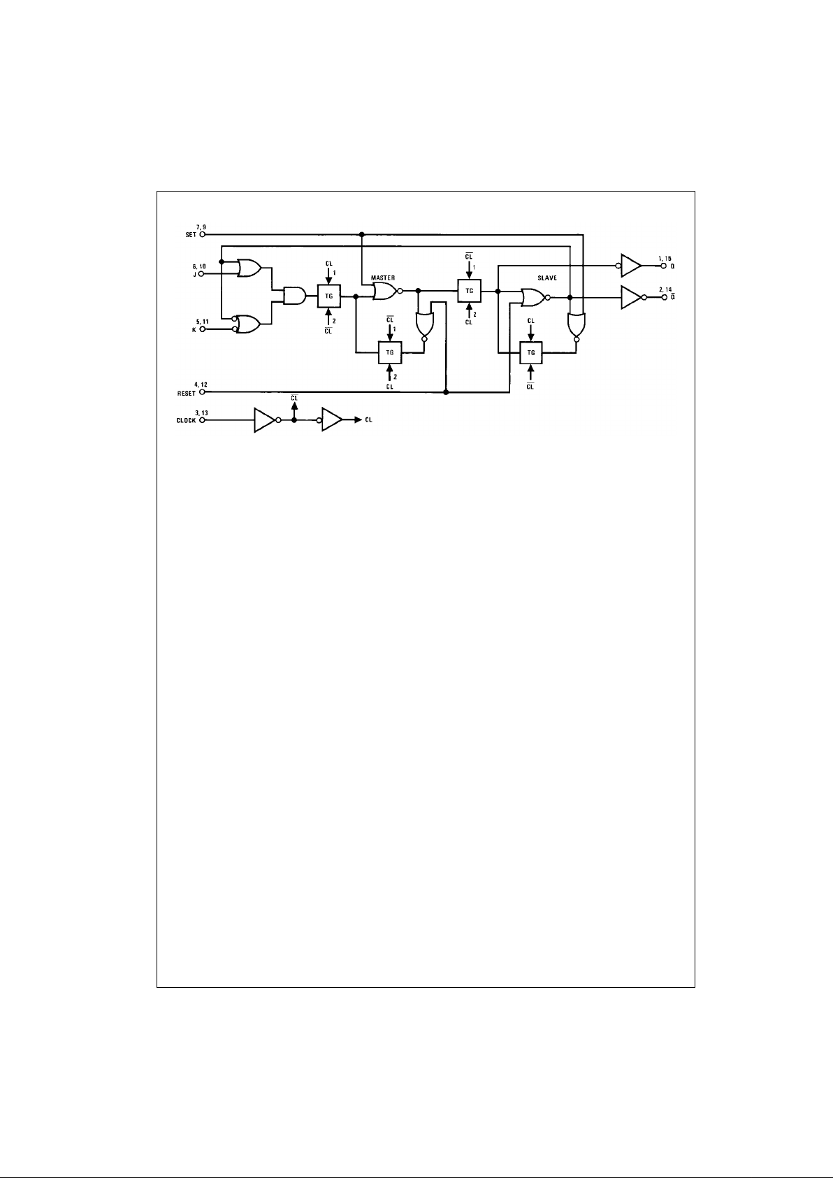
Logic Diagram
Page 3

3 www.fairchildsemi.com
CD4027BC
Absolute Maximum Ratings(Note 4)
(Note 5)
Recommended Operating
Conditions
(Note 5)
Note 4: “Absolute Maximum Rat ings” are tho se values beyond which the
safety of the device cannot be guaranteed. They are not meant to imply
that the devices should be op erated at these lim its. The table of “Recommended Operating Conditions” and “Electrical Characteristics” provides
conditions for actual device o peration.
Note 5: V
SS
= 0V unless otherw is e s pecified.
DC Electrical Characteristics (Note 6)
Note 6: VSS = 0V unless otherwise specified.
Note 7: I
OH
and IOL are tested one output at a ti m e.
DC Supply Voltage (VDD) −0.5 VDC to +18 V
DC
Input Voltage (VIN) −0.5V to VDD +0.5 V
DC
Storage Temperature Range (TS) −65°C to +150°C
Power Dissipa tion (P
D
)
Dual-In-Line 700 mW
Small Outline 500 mW
Lead Temperature (T
L
)
(Soldering, 10 seconds) 260°C
DC Supply Voltage (V
DD
) 3V to 15 V
DC
Input Voltage (VIN) 0V to VDD V
DC
Operating Temperature Range (TA) −40°C to +85°C
Symbol Parameter Conditions
−40°C +25°C +85°C
Units
Min Max Min Typ Max Min Max
I
DD
Quiescent Device Current VDD = 5V, VIN = VDD or V
SS
4430µA
VDD = 10V, VIN = VDD or V
SS
8860µA
VDD = 15V, VIN = VDD or V
SS
16 16 120 µA
V
OL
LOW Level |IO| < 1 µA
Output Voltage VDD = 5V 0.05 0 0.05 0.05 V
VDD = 10V 0.05 0 0.05 0.05 V
VDD = 15V 0.05 0 0.05 0.05 V
V
OH
HIGH Level |IO| < 1 µA
Output Voltage VDD = 5V 4.95 4.95 5 4.95 V
VDD = 10V 9.95 9.95 10 9.95 V
VDD = 15V 14.95 14.95 15 14.95 V
V
IL
LOW Level VDD = 5V, VO = 0.5V or 4.5V 1.5 1.5 1.5 V
Input Voltage VDD = 10V, VO = 1V or 9V 3.0 3.0 3.0 V
VDD = 15V, VO = 1.5V or 13.5V 4.0 4.0 4.0 V
V
IH
HIGH Level VDD = 5V, VO = 0.5V or 4.5V 3.5 3.5 3.5 V
Input Voltage VDD = 10V, VO = 1V or 9V 7.0 7.0 7.0 V
VDD = 15V, VO = 1.5V or 13.5V 11.0 11.0 11.0 V
I
OL
LOW Level Output VDD = 5V, VO = 0.4V 0.52 0.44 0.88 0.36 mA
Current (Note 7) VDD = 10V, VO = 0.5V 1.3 1.1 2.25 0.9 mA
VDD = 15V, VO = 1.5V 3.6 3.0 8.8 2.4 mA
I
OH
HIGH Level Output VDD = 5V, VO = 4.6V −0.52 −0.44 −0.88 −0.36 mA
Current (Note 7) VDD = 10V, VO = 9.5V −1.3 −1.1 −2.25 −0.9 mA
VDD = 15V, VO = 13.5V −3.6 −3.0 −8.8 −2.4 mA
I
IN
Input Current VDD = 15V, VIN = 0V −0.3 −10−5−0.3 −1.0 µA
VDD = 15V, VIN = 15V 0.3 10−50.3 1.0 µA
Page 4

www.fairchildsemi.com 4
CD4027BC
AC Electrical Charac teristics (Note 8)
TA = 25°C, CL = 50 pF, t
rCL
= t
fCL
= 20 ns, unless otherwise specified
Note 8: AC Parameters are guara nt eed by DC correlated testin g.
Note 9: C
PD
determines the no lo ad AC power consump tion of any CMOS device. For comple te explanatio n, see 74C Family Ch aracteris tics application
note, AN-90.
Typical Applications
Ripple Binary Counters
Shift Registers
Symbol Parameter Conditions Min Typ Max Units
t
PHL
or t
PLH
Propagation Delay Time VDD = 5V 200 400 ns
from Clock to Q or Q VDD = 10V 80 160 ns
VDD = 15V 65 130 ns
t
PHL
or t
PLH
Propagation Delay Time VDD = 5V 170 340 ns
from Set to Q or Reset to Q VDD = 10V 70 140 ns
VDD = 15V 55 110 ns
t
PHL
or t
PLH
Propagation Delay Time VDD = 5V 110 220 ns
from Set to Q or VDD = 10V 50 100 ns
Reset to Q VDD = 15V 40 80 ns
t
S
Minimum Data Setup Time VDD = 5V 135 270 ns
VDD = 10V 55 110 ns
VDD = 15V 45 90 ns
t
THL
or t
TLH
Transition Time VDD = 5V 100 200 ns
VDD = 10V 50 100 ns
VDD = 15V 40 80 ns
f
CL
Maximum Clock Frequency VDD = 5V 2.5 5 MHz
(Toggle Mode) VDD = 10V 6.2 12.5 MHz
VDD = 15V 7.6 15.5 MHz
t
rCL
or t
fCL
Maximum Clock Rise VDD = 5V 15 µs
and Fall Time VDD = 10V 10 µs
VDD = 15V 5 µs
t
W
Minimum Clock Pulse VDD = 5V 100 200 ns
Width (tWH = tWL)V
DD
= 10V 40 80 ns
VDD = 15V 32 65 ns
t
WH
Minimum Set and VDD = 5V 80 160 ns
Reset Pulse Width VDD = 10V 30 60 ns
VDD = 15V 25 50 ns
C
IN
Average Input Capacitance Any Input 5 7.5 pF
C
PD
Power Dissipation Capacity Per Flip-Flop 35 pF
(Note 9)
Page 5

5 www.fairchildsemi.com
CD4027BC
Physical Dimensions inches (millimeters) unless otherwise noted
16-Lead Small Outline Integrated Circuit (SOIC), JEDEC MS-012, 0.150” Narrow Body
Package Number M16A
Page 6

Fairchild does not assume any responsibility for use of any circuitry descri bed, no circuit patent licenses are implied and Fairchil d reser ves the right at any time without notice to change said circuitr y and specifications.
CD4027BC Dual J-K Master/Slave Flip-Flop with Set and Reset
LIFE SUPPORT POLICY
FAIRCHILD’S PRODUCTS ARE NOT AUTHORIZED FOR USE AS CRITICAL COMPONENTS IN LIFE SUPPORT
DEVICES OR SYSTEMS WITHOUT THE EXPRESS WRITTEN APPROVAL OF THE PRESIDENT OF FAIRCHILD
SEMICONDUCTOR CORPORATION. As used herein:
1. Life support devices or systems are devices or syste ms
which, (a) are intended for surgical implant into the
body, or (b) support or sustain life, and (c) whose failure
to perform when properly used in accordance with
instructions for use provided in the labeling, can be reasonably expected to result in a significant injury to the
user.
2. A critical comp onent in any comp onent of a li fe suppor t
device or system whose failure to perform can be reasonably expected to cause the failure of the life suppor t
device or system, or to affect its safety or effectiveness.
www.fairchildsemi.com
Physical Dimensions inches (millimeters) unless otherwise noted (Continued)
16-Lead Plastic Dual-In-Line Package (PDIP), JEDEC MS-001, 0.300” Wide
Package Number N16E
 Loading...